


-
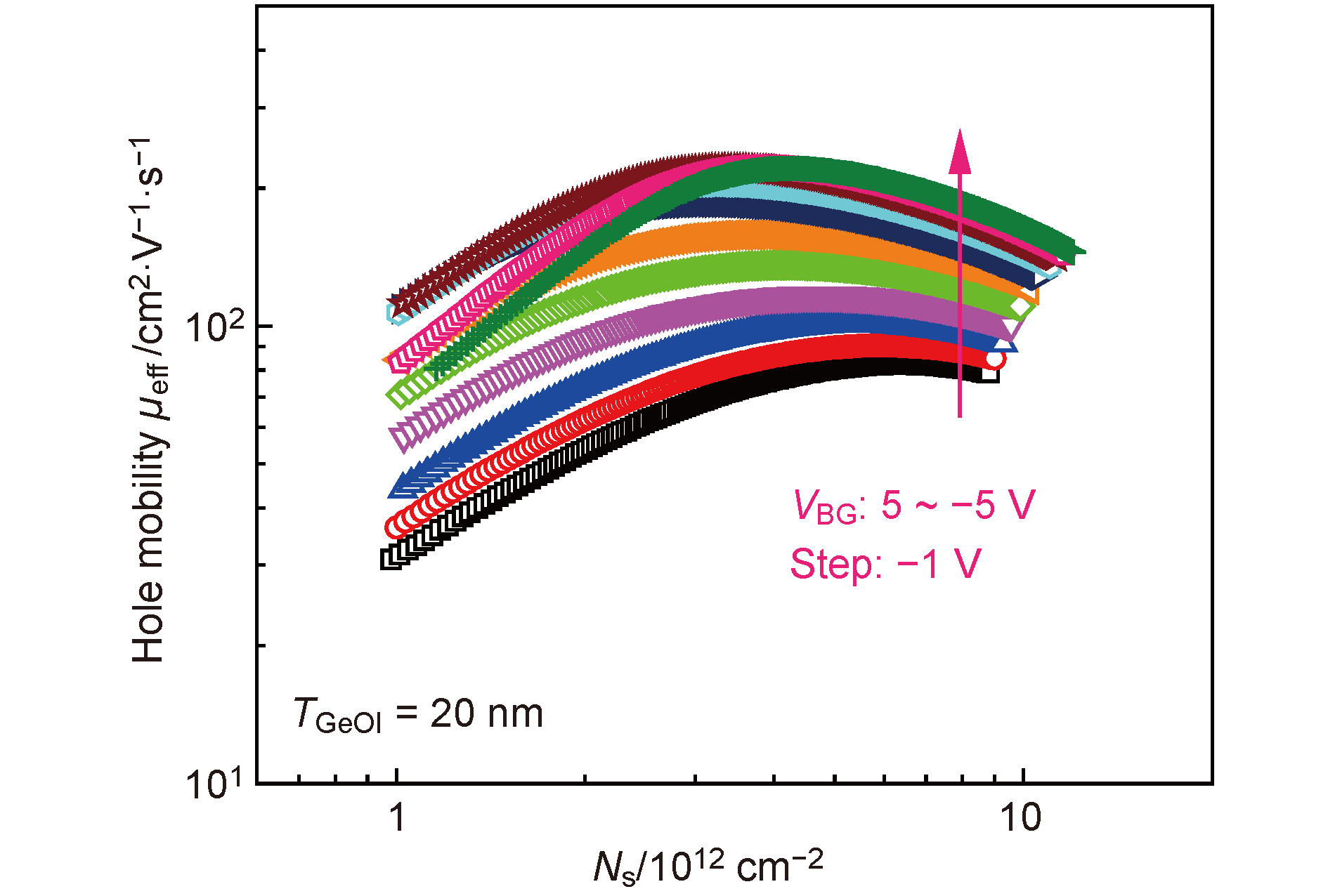
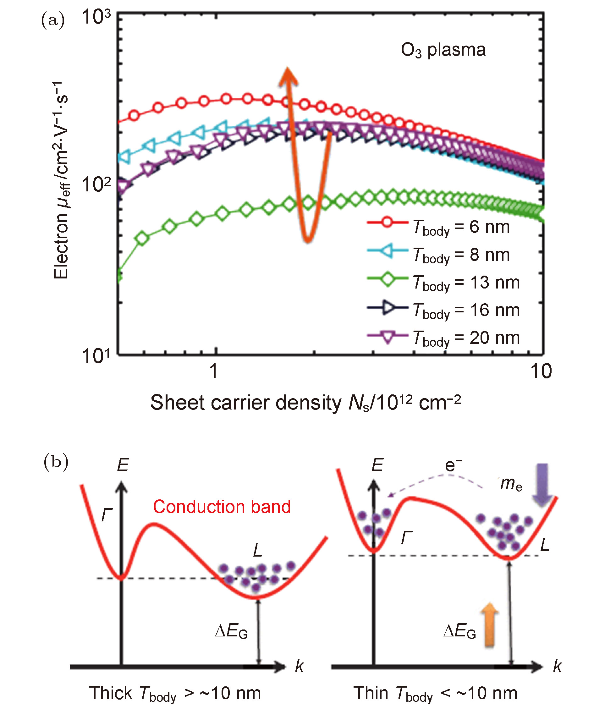
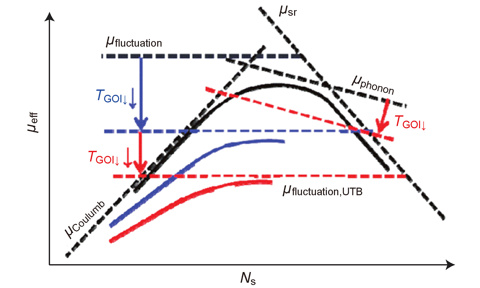
As the feature size of Metal-Oxide-Semiconductor Field Effect Transistors (MOSFETs) continues to decrease, large numbers of new problems appear. Techniques such as strain project, new channel materials and new device structures are considered by academics and industry to be effective ways to continue to improve device performance. In this paper, the scattering mechanism of carriers in the device channel is studied from three aspects: strain technique, new channel material and new structure device: (1) strain technique: Biaxial tensile strain can change carrier distribution among different energy levels, which affects Coulomb scattering and Coulomb mobility. Furthermore, from the TEM image, it is found that biaxial tensile reduces the channel surface roughness for Si nMOSFET, leading an enhancement of electron mobility. However, no such similar phenomena were observed in pMOSFET. Based on this, a new method for calculating the mobility of MOSFET surface roughness scattering using TEM image has been proposed. (2) New channel material: In the germanium (Ge) transistors with different crystal faces, the scattering mechanisms of electron under high field conditions are different. The phonon scattering dominates the Ge(100) transistor, while the surface roughness scattering dominates the Ge(110), (111) transistors. This result is quite different from Si MOSFET. Therefore, a unified model for the scattering mechanism of electron in Ge nMOSFET has been proposed. In SiGe transistors, alloy scattering mainly play a role in the region with relatively small effective electric field (Eeff). The strength of alloy scattering would be weakened in high field and could be decreased by reducing the thickness of SiGe layer. (3) New structure devices: In ultra-thin body germanium (GeOI) transistors, carrier transport is influenced by high- k /channel interfaces, as well as Ge channel/buried oxide (BOX) interface. As the Ge layer thickness decreases, carrier distribution is closer to the interfaces, which intensifies Coulomb scattering and surface roughness scattering. As a result, the mobility in GeOI transistor decreases as the thickness scaling. In addition, the distribution of electron in different energy valleys changes with the thickness decrease in Ge layer, which affects the scattering of electrons. When the Ge film is lower than 10 nm, a part of electron in the L valley will move to the Γ valley, causing the decrease of electron effective mass and increasing the electron mobility.
[1] Uchida K, Takagi S 2003 Appl. Phys. Lett. 82 2916
 Google Scholar
[2] Wu H, Wu W, Si M, Peide D Y 2015 IEEE International Electron Devices Meeting (IEDM) Washington DC, Dec. 7−9, 2015 p2.1.1
[3] Nayak D K, Woo J C S, Park J S, Wang K L, MacWilliams K P 1993 Appl. Phys. Lett. 62 2853
Google Scholar
[4] 刘畅、卢继武、吴汪然、唐晓雨、张睿、俞文杰、王曦、赵毅 2015 物理学报 62 167305
Liu C, Lu J W, Wu W R, Tang X Y, Zhang R, Yu W J, Wang X, Zhao Y 2015 Acta Phys. Sin. 62 167305
[5] 赵毅、万星拱 2006 物理学报 55 3003
Zhao Y, Wan X G 2006 Acta Phys. Sin. 55 3003
[6] Lee C H, Nishimura T, Tabata T, Lu C, Zhang W F, Nagashio K, Toriumi A 2013 IEEE International Electron Devices Meeting (IEDM) Washington DC, Dec. 9−11, 2013 p2.3.1
[7] Cheng R, Yin L, Wu H, Yu X, Zhang Y, Zheng Z, Wu W, Chen B, Peide D Y, Liu X, Zhao Y 2017 IEEE Elec. Devi. Lett. 38 434
Google Scholar
[8] Chu M, Sun Y, Aghoram U, Thompson S E 2009 Annu. Rev. Mater. Res. 39 203
Google Scholar
[9] Antoniadis D A, Aberg I, Chleirigh C N, Nayfeh O M, Khakifirooz A, Hoyt J L 2006 IBM J. Res. Dev. 50 363
Google Scholar
[10] Lee C H, Nishimura T, Tabata T, Kita K, Toriumi A 2011 IEEE Trans. Elec. Dev. 58 1295
[11] Zhang, R, Huang P C, Lin J C, Taoka N, Takenaka M, Takagi S 2013 IEEE Trans. Elec.n Dev. 60 927
[12] Zhang R, Chern W, Yu X, Takenaka, M, Hoyt J L, Takagi, S 2013 IEEE International Electron Devices Meeting (IEDM) Washington DC, Dec. 9−11 2013 p26.1.1
[13] Yeo Y C, Gong X, van Dal M J H, Vellianitis G, Passlack M 2015 IEEE International Electron Devices Meeting (IEDM) Washington D C, Dec. 7−9,2015 p2.4.1
[14] van Dal M J H, Duriez B, Vellianitis G, Doornbos G, Oxland R, Holland M, Diaz C H 2014 IEEE International Electron Devices Meeting (IEDM) San Francisco, Dec. 7−9, 2014 p9.5.1
[15] Choi Y K, Asano K, Lindert N, Subramanian V, King T J, Bokor J, Hu C 1999 IEEE International Electron Devices Meeting (IEDM) Washington D C, Dec. 5−8, 1999 p919
[16] Ernst T, Cristoloveanu S, Ghibaudo G, Ouisse T, Horiguchi S, Ono Y, Takahashi Y, Murase K 2003 IEEE Trans. Elec. Dev. 50 830
[17] Zhao Y, Takenaka M, Takagi S 2009 IEEE Trans. Elec. Dev. 56 1152
Google Scholar
[18] Weber O, Takagi S 2008 IEEE Trans. Elec. Dev. 55 2386
[19] Takagi S, Toriumi A, Iwase M, Tango H 1994 IEEE Trans. Elec. Dev. 41 2357
Google Scholar
[20] Zhao Y, Takenaka M, Takagi S 2009 IEEE Elec. Dev. Lett. 30 987
Google Scholar
[21] Zhao Y, Matsumoto H, Sato T, Koyama S, Takenaka M, Takagi S 2010 IEEE Trans. Elec. Dev. 57 2057
Google Scholar
[22] Wu W, Li X, Sun J, Zhang R, Shi Y, Zhao Y 2015 IEEE Trans. Elec. Dev. 62 1136
Google Scholar
[23] Yu W, Wu W, Zhang B, Liu C, Sun J, Zhai D, Yu Y, Shi Y, Zhao Y, Zhao Q T 2014 IEEE Trans. Elec. Dev. 61 950
Google Scholar
[24] Yu X, Kang J, Takenaka M, Takagi S 2015 IEEE International Electron Devices Meeting (IEDM) Washington D C, Dec. 7−9, 2015 p2.2.1
[25] Zheng Z, Yu X, Zhang Y, Xie M, Cheng R, Zhao Y 2018 IEEE Trans. Elec. Dev. 65 895
Google Scholar
[26] Chang W H, Irisawa T, Ishii H, Hattori H, Ota H, Takagi H, Kurashima Y, Uchida K, Maeda T 2017 IEEE Trans. Elec. Dev. 64 4615
Google Scholar
-
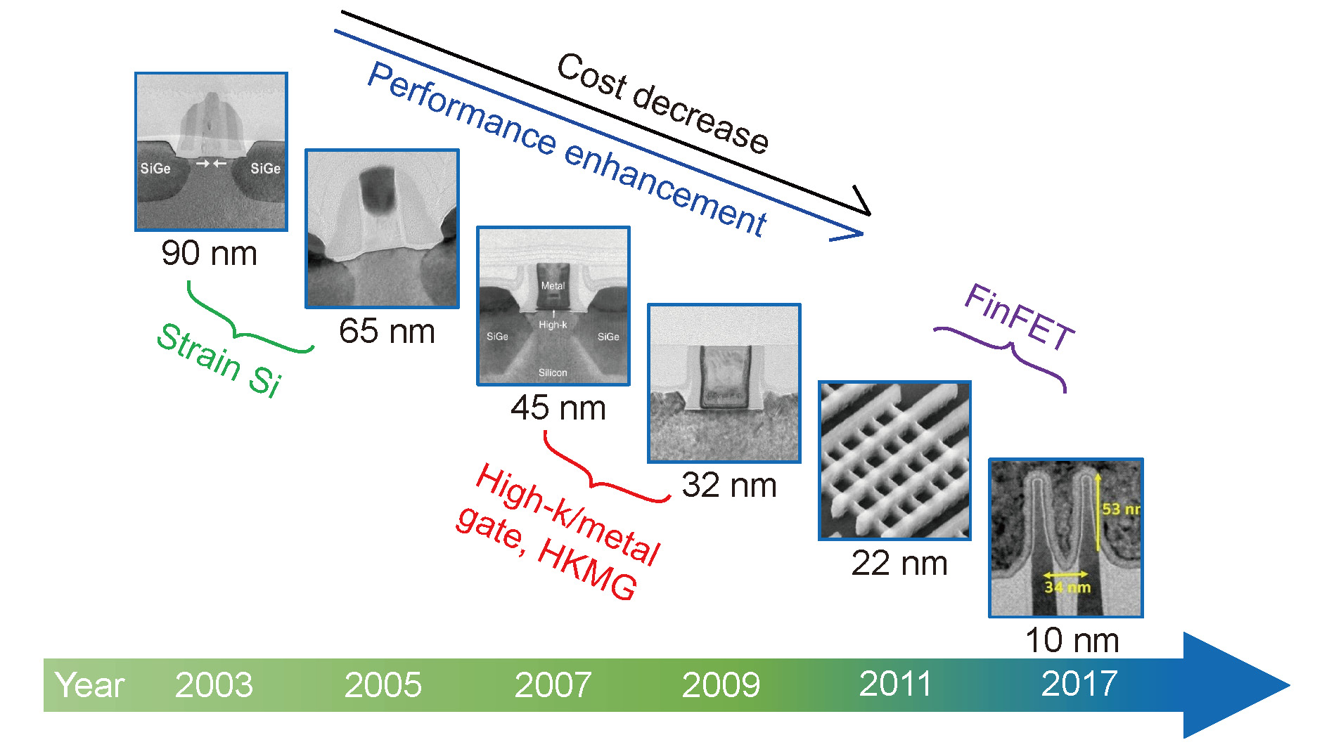
图 1 集成电路技术节点随时间的演进, 图中提取了90 nm到10 nm技术节点
Figure 1. Evolution of integrated circuit technology nodes: from 90 nm to 10 nm.

-
[1] Uchida K, Takagi S 2003 Appl. Phys. Lett. 82 2916
Google Scholar
[2] Wu H, Wu W, Si M, Peide D Y 2015 IEEE International Electron Devices Meeting (IEDM) Washington DC, Dec. 7−9, 2015 p2.1.1
[3] Nayak D K, Woo J C S, Park J S, Wang K L, MacWilliams K P 1993 Appl. Phys. Lett. 62 2853
Google Scholar
[4] 刘畅、卢继武、吴汪然、唐晓雨、张睿、俞文杰、王曦、赵毅 2015 物理学报 62 167305
Liu C, Lu J W, Wu W R, Tang X Y, Zhang R, Yu W J, Wang X, Zhao Y 2015 Acta Phys. Sin. 62 167305
[5] 赵毅、万星拱 2006 物理学报 55 3003
Zhao Y, Wan X G 2006 Acta Phys. Sin. 55 3003
[6] Lee C H, Nishimura T, Tabata T, Lu C, Zhang W F, Nagashio K, Toriumi A 2013 IEEE International Electron Devices Meeting (IEDM) Washington DC, Dec. 9−11, 2013 p2.3.1
[7] Cheng R, Yin L, Wu H, Yu X, Zhang Y, Zheng Z, Wu W, Chen B, Peide D Y, Liu X, Zhao Y 2017 IEEE Elec. Devi. Lett. 38 434
Google Scholar
[8] Chu M, Sun Y, Aghoram U, Thompson S E 2009 Annu. Rev. Mater. Res. 39 203
Google Scholar
[9] Antoniadis D A, Aberg I, Chleirigh C N, Nayfeh O M, Khakifirooz A, Hoyt J L 2006 IBM J. Res. Dev. 50 363
Google Scholar
[10] Lee C H, Nishimura T, Tabata T, Kita K, Toriumi A 2011 IEEE Trans. Elec. Dev. 58 1295
[11] Zhang, R, Huang P C, Lin J C, Taoka N, Takenaka M, Takagi S 2013 IEEE Trans. Elec.n Dev. 60 927
[12] Zhang R, Chern W, Yu X, Takenaka, M, Hoyt J L, Takagi, S 2013 IEEE International Electron Devices Meeting (IEDM) Washington DC, Dec. 9−11 2013 p26.1.1
[13] Yeo Y C, Gong X, van Dal M J H, Vellianitis G, Passlack M 2015 IEEE International Electron Devices Meeting (IEDM) Washington D C, Dec. 7−9,2015 p2.4.1
[14] van Dal M J H, Duriez B, Vellianitis G, Doornbos G, Oxland R, Holland M, Diaz C H 2014 IEEE International Electron Devices Meeting (IEDM) San Francisco, Dec. 7−9, 2014 p9.5.1
[15] Choi Y K, Asano K, Lindert N, Subramanian V, King T J, Bokor J, Hu C 1999 IEEE International Electron Devices Meeting (IEDM) Washington D C, Dec. 5−8, 1999 p919
[16] Ernst T, Cristoloveanu S, Ghibaudo G, Ouisse T, Horiguchi S, Ono Y, Takahashi Y, Murase K 2003 IEEE Trans. Elec. Dev. 50 830
[17] Zhao Y, Takenaka M, Takagi S 2009 IEEE Trans. Elec. Dev. 56 1152
Google Scholar
[18] Weber O, Takagi S 2008 IEEE Trans. Elec. Dev. 55 2386
[19] Takagi S, Toriumi A, Iwase M, Tango H 1994 IEEE Trans. Elec. Dev. 41 2357
Google Scholar
[20] Zhao Y, Takenaka M, Takagi S 2009 IEEE Elec. Dev. Lett. 30 987
Google Scholar
[21] Zhao Y, Matsumoto H, Sato T, Koyama S, Takenaka M, Takagi S 2010 IEEE Trans. Elec. Dev. 57 2057
Google Scholar
[22] Wu W, Li X, Sun J, Zhang R, Shi Y, Zhao Y 2015 IEEE Trans. Elec. Dev. 62 1136
Google Scholar
[23] Yu W, Wu W, Zhang B, Liu C, Sun J, Zhai D, Yu Y, Shi Y, Zhao Y, Zhao Q T 2014 IEEE Trans. Elec. Dev. 61 950
Google Scholar
[24] Yu X, Kang J, Takenaka M, Takagi S 2015 IEEE International Electron Devices Meeting (IEDM) Washington D C, Dec. 7−9, 2015 p2.2.1
[25] Zheng Z, Yu X, Zhang Y, Xie M, Cheng R, Zhao Y 2018 IEEE Trans. Elec. Dev. 65 895
Google Scholar
[26] Chang W H, Irisawa T, Ishii H, Hattori H, Ota H, Takagi H, Kurashima Y, Uchida K, Maeda T 2017 IEEE Trans. Elec. Dev. 64 4615
Google Scholar

 DownLoad:
Catalog
Metrics
- Abstract views: 9880
- PDF Downloads: 163
- Cited By: 0
