


-
Ohmic contact is directly related to the performance of GaN device and is one of the important factors affecting device performance. In recent years, many research groups have studied the electrode materials and annealing conditions of n-type GaN Ohmic contacts. In this paper, the ohmic contact properties and structural characteristics of the Hf/Al electrode of a transition group metal refractory metal Hf system under different annealing conditions are studied, and compared with those of the Ti-based ohmic contact Ti/Al electrode. The specific contact resistivity of each electrode is measured by a dot-type transmission line model, and the structural characteristics of the electrode are analyzed by using an Auger electron spectrometer which can be analyzed in depth. The results show that the Hf/Al electrode under the same annealing condition exhibits superior ohmic contact performance compared with the conventional Ti/Al electrode. At the same time, the lowest specific contact resistivity of the Hf/Al electrode annealed in an N2 atmosphere at a low temperature of 650 ℃ for 60 s is 4.28×10⁻⁵ Ω·cm2. The in-depth analysis of Auger electron spectrum shows that the Hf/Al electrode has a solid phase reaction with the n-type GaN material. In addition, the cross section of each electrode is observed by auger electron spectroscopy. In the Hf/Al electrode sample, the metal-semiconductor interface does not show voids after annealing. This situation occurs at the sample interface where the Ti/Al electrode is annealed at 650 ℃ for 60 s in N2 atmosphere and annealed at 850 ℃ for 30 s in N2 atmosphere. This is one of the reasons why the Hf/Al electrode sample has a lower specific contact resistivity. At the same time, the surface of Hf/Al electrode and Ti/Al electrode annealed at 850 ℃ are characterized by using scanning electron microscope. It is found that the surfaces of both electrodes subject to high temperature annealing show a similar granular rough surface, and this rough surface has a certain influence on the electrical properties of the GaN device. The rough surface formed by the electrode under such high temperature annealing conditions is an urgent problem to be solved in the future research. In summary, the study in this paper indicates the use of Hf/Al to form an ohmic contact with n-type GaN under a low temperature annealing condition.
-
Keywords:
- n-type GaN /
- Ohmic contact /
- rapid thermal annealing /
- hafnium
[1] Strite S, Morka Strite S, Morkoç H 1992 J. Vac. Sci. Technol. B: Microelectron Process Phenom 10 1237
 Google Scholar
[2] Davydov V Y, Klochikhin A, Emtsev V V, Kurdyukov D, Ivanov S, Vekshin V, Bechstedt F, Furthmüller J, Aderhold J, Graul J 2002 Phys. Status Solidi B 234 787
Google Scholar
[3] Pearton S, Ren F, Zhang A, Lee K 2000 Mater. Sci. Eng. R. Rep. 30 55
Google Scholar
[4] Munoz E, Monroy E, Pau J, Calle F, Omnes F, Gibart P 2001 J. Phys. Condens. Matter 13 7115
Google Scholar
[5] Deger C, Born E, Angerer H, Ambacher O, Stutzmann M, Hornsteiner J, Riha E, Fischerauer G 1998 Appl. Phys. Lett. 72 2400
Google Scholar
[6] Huang Z, Goldberg R, Chen J, Zheng Y, Mott D B, Shu P 1995 Appl. Phys. Lett. 67 2825
Google Scholar
[7] Pimputkar S, Speck J S, DenBaars S P, Nakamura S 2009 Nat. Photonics 3 180
Google Scholar
[8] Ruvimov S, Liliental Z, Washburn J, Duxstad K, Haller E, Fan Z F, Mohammad S N, Kim W, Botchkarev A, Morkoc H 1996 Appl. Phys. Lett. 69 1556
Google Scholar
[9] Wang D F, Shiwei F, Lu C, Motayed A, Jah M, Mohammad S N, Jones K A, Salamanca-Riba L 2001 J. Appl. Phys. 89 6214
Google Scholar
[10] Selvanathan D, Zhou L, Kumar V, Adesida I 2002 Phys. Status Solidi B (a)
194 583 Google Scholar
[11] Iucolano F, Roccaforte F, Alberti A, Bongiorno C, Di Franco S, Raineri V 2006 J. Appl. Phys. 100 123706
Google Scholar
[12] Zhang T, Pu T, Xie T, Li L, Bu Y, Wang X, Ao J P 2018 Chin. Phys. B 27 078503
Google Scholar
[13] Yao J N, Lin Y C, Chuang Y L, Huang Y X, Shih W C, Sze S M, Chang E Y 2015 IEEE 22nd International Symposium on the Physical and Failure Analysis of Integrated Circuits (Hsinchu) p419
[14] Singh K, Chauhan A, Mathew M, Punia R, Meena S S, Gupta N, Kundu R S 2019 Appl. Phys. A 125 24
[15] Shostachenko S, Porokhonko Y, Zakharchenko R, Burdykin M, Ryzhuk R, Kargin N, Kalinin B, Belov A, Vasiliev A 2017 J. Phys. Conf. Ser. 938 012072
[16] van Daele B, van Tendeloo G, Ruythooren W, Derluyn J, Leys M, Germain M 2005 Appl. Phys. Lett. 87 061905
Google Scholar
[17] Landolt H, Börnstein R, Predel B 1991 Phase Equilibria, Crystallographic and Thermodynamic Data of Binary Alloys (Vol. 5) (Berlin: Springer) pp4–6
[18] Gong R, Wang J, Liu S, Dong Z, Yu M, Wen C P, Cai Y, Zhang B 2010 Appl. Phys. Lett. 97 062115
Google Scholar
[19] Greco G, Iucolano F, Roccaforte F 2016 Appl. Surface Sci. 383 324
Google Scholar
[20] France R, Xu T, Chen P, Chandrasekaran R, Moustakas T 2007 Appl. Phys. Lett. 90 062115
Google Scholar
[21] Park J S, Han J, Seong T Y 2015 J. Alloys Compd. 652 167
Google Scholar
[22] Zhao S, Gao J, Wang S, Xie H, Ponce F A, Goodnick S, Chowdhury S 2017 Jpn. J. Appl. Phys. 56 126502
Google Scholar
[23] Kurtin S, McGill T, Mead C 1969 Phys. Rev. Lett. 22 1433
Google Scholar
[24] Michaelson H B 1977 J. Appl. Phys. 48 4729
Google Scholar
[25] Bass J 1982 Landolt-Börnstein-Group Ⅲ Condensed Matter (Berlin: Springer) pp5–13
[26] Mohammad S N 2004 J. Appl. Phys. 95 7940
Google Scholar
-

图 1 目前最常应用于n型GaN欧姆接触的Ti基多层金属体系
Figure 1. Ti-based multilayer metal system most commonly used in n-type GaN ohmic contact

图 2 实验中用到的圆点型传输线模型(dot CTLM)结构
Figure 2. The scheme of dot circular transmission line model (dot CTLM) in this experiment
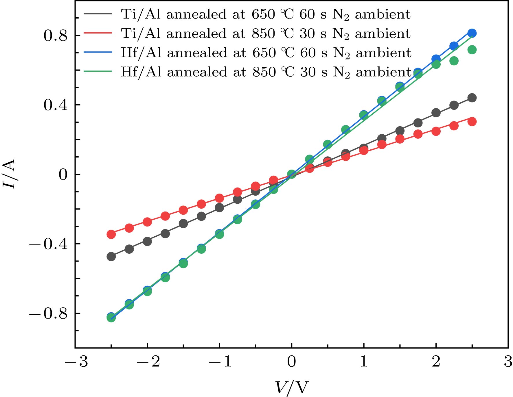
图 3 不同退火条件下Ti/Al, Hf/Al样品间距为10 μm的电极之间的I-V曲线
Figure 3. I-V curve between Ti/Al, Hf/Al pads with 10 μm spacing anneales at different condition.

图 4 Hf/Al电极样品深度剖析的AES图 (a)未退火; (b) 650 ℃退火60 s
Figure 4. AES depth profiles of Hf/Al electrodes: (a) No annealing and (b) after annealing at 650 ℃ for 60 s in N2 ambient.
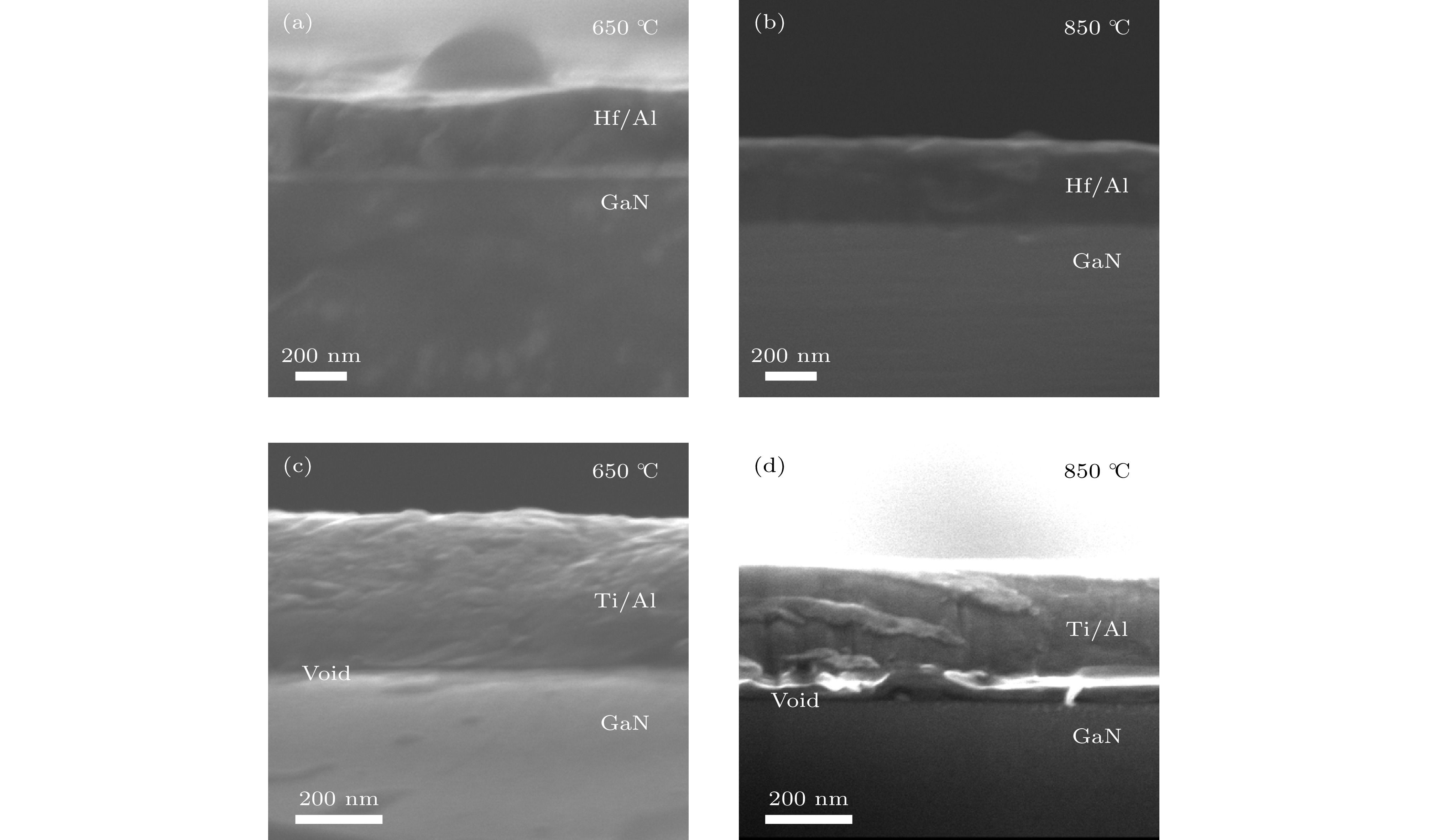
图 5 各电极的截面SEM图像 (a) Hf/Al, 650 ℃; (b) Hf/Al, 850 ℃; (c) Ti/Al, 650 ℃; (d) Ti/Al, 850 ℃
Figure 5. Cross-sectional SEM image of each electrode: (a) Hf/Al, 650 ℃; (b) Hf/Al, 850 ℃; (c) Ti/Al, 650 ℃; (d) Ti/Al, 850 ℃

图 6 各电极在850 ℃条件下退火的表面SEM图 (a) Hf/Al; (b) Ti/Al
Figure 6. SEM image of each electrode annealed at 850 ℃ condition: (a) Hf/Al; (b) Ti/Al
表 1 不同金属的功函数、熔点、电阻率 (273 K)
Table 1. Work function, melting point and resi-stivity of different metals.
 DownLoad: CSV
表 2 各电极样品在不同退火条件下的比接触电阻率
Table 2. Specific contact resistivity of each electrode sample at different annealing conditions.
样品名称 退火条件 (N2) 比接触电阻率/Ω·cm2 Hf/Al no annealing 1.21×10⁻⁴ Hf/Al 650 ℃ 60 s 4.28×10⁻⁵ Hf/Al 850 ℃ 30 s 1.13×10⁻⁴ Ti/Al 650 ℃ 60 s 5.85×10⁻⁵ Ti/Al 850 ℃ 30 s 1.27×10⁻⁴
DownLoad: CSV
-
[1] Strite S, Morka Strite S, Morkoç H 1992 J. Vac. Sci. Technol. B: Microelectron Process Phenom 10 1237
Google Scholar
[2] Davydov V Y, Klochikhin A, Emtsev V V, Kurdyukov D, Ivanov S, Vekshin V, Bechstedt F, Furthmüller J, Aderhold J, Graul J 2002 Phys. Status Solidi B 234 787
Google Scholar
[3] Pearton S, Ren F, Zhang A, Lee K 2000 Mater. Sci. Eng. R. Rep. 30 55
Google Scholar
[4] Munoz E, Monroy E, Pau J, Calle F, Omnes F, Gibart P 2001 J. Phys. Condens. Matter 13 7115
Google Scholar
[5] Deger C, Born E, Angerer H, Ambacher O, Stutzmann M, Hornsteiner J, Riha E, Fischerauer G 1998 Appl. Phys. Lett. 72 2400
Google Scholar
[6] Huang Z, Goldberg R, Chen J, Zheng Y, Mott D B, Shu P 1995 Appl. Phys. Lett. 67 2825
Google Scholar
[7] Pimputkar S, Speck J S, DenBaars S P, Nakamura S 2009 Nat. Photonics 3 180
Google Scholar
[8] Ruvimov S, Liliental Z, Washburn J, Duxstad K, Haller E, Fan Z F, Mohammad S N, Kim W, Botchkarev A, Morkoc H 1996 Appl. Phys. Lett. 69 1556
Google Scholar
[9] Wang D F, Shiwei F, Lu C, Motayed A, Jah M, Mohammad S N, Jones K A, Salamanca-Riba L 2001 J. Appl. Phys. 89 6214
Google Scholar
[10] Selvanathan D, Zhou L, Kumar V, Adesida I 2002 Phys. Status Solidi B (a)
194 583 Google Scholar
[11] Iucolano F, Roccaforte F, Alberti A, Bongiorno C, Di Franco S, Raineri V 2006 J. Appl. Phys. 100 123706
Google Scholar
[12] Zhang T, Pu T, Xie T, Li L, Bu Y, Wang X, Ao J P 2018 Chin. Phys. B 27 078503
Google Scholar
[13] Yao J N, Lin Y C, Chuang Y L, Huang Y X, Shih W C, Sze S M, Chang E Y 2015 IEEE 22nd International Symposium on the Physical and Failure Analysis of Integrated Circuits (Hsinchu) p419
[14] Singh K, Chauhan A, Mathew M, Punia R, Meena S S, Gupta N, Kundu R S 2019 Appl. Phys. A 125 24
[15] Shostachenko S, Porokhonko Y, Zakharchenko R, Burdykin M, Ryzhuk R, Kargin N, Kalinin B, Belov A, Vasiliev A 2017 J. Phys. Conf. Ser. 938 012072
[16] van Daele B, van Tendeloo G, Ruythooren W, Derluyn J, Leys M, Germain M 2005 Appl. Phys. Lett. 87 061905
Google Scholar
[17] Landolt H, Börnstein R, Predel B 1991 Phase Equilibria, Crystallographic and Thermodynamic Data of Binary Alloys (Vol. 5) (Berlin: Springer) pp4–6
[18] Gong R, Wang J, Liu S, Dong Z, Yu M, Wen C P, Cai Y, Zhang B 2010 Appl. Phys. Lett. 97 062115
Google Scholar
[19] Greco G, Iucolano F, Roccaforte F 2016 Appl. Surface Sci. 383 324
Google Scholar
[20] France R, Xu T, Chen P, Chandrasekaran R, Moustakas T 2007 Appl. Phys. Lett. 90 062115
Google Scholar
[21] Park J S, Han J, Seong T Y 2015 J. Alloys Compd. 652 167
Google Scholar
[22] Zhao S, Gao J, Wang S, Xie H, Ponce F A, Goodnick S, Chowdhury S 2017 Jpn. J. Appl. Phys. 56 126502
Google Scholar
[23] Kurtin S, McGill T, Mead C 1969 Phys. Rev. Lett. 22 1433
Google Scholar
[24] Michaelson H B 1977 J. Appl. Phys. 48 4729
Google Scholar
[25] Bass J 1982 Landolt-Börnstein-Group Ⅲ Condensed Matter (Berlin: Springer) pp5–13
[26] Mohammad S N 2004 J. Appl. Phys. 95 7940
Google Scholar

 DownLoad:
Catalog
Metrics
- Abstract views: 8324
- PDF Downloads: 81
- Cited By: 0
