


-
Organometal halide perovskites featuring solution-processable characteristics, high photoluminescence quantum yield (PLQY), and color purity, are an emerging class of semiconductor with considerable potential applications in optoelectronic devices. Electron injection layer is an important component of perovskite light-emitting device, which determines the growth of perovskite film directly. In this paper, the perovskite light-emitting diodes (PeLEDs) based on n-type nanocrystalline silicon oxide (n-nc-SiOx:H) electron injection layer are designed and realized. This novel electron injecting material is prepared by the plasma enhanced chemical vapor deposition (PECVD), and its smooth surface and matched energy band result in superior perovskite crystallinity and low electron injection barrier from the electron injecting layer to the emissive layer, respectively. However, the external quantum efficiency (EQE) of PeLED is as low as 0.43%, which relates to defects and leakage current due to the incomplete surface coverage of perovskite film. The fast exciton emission decay (< 10 ns) stems from strong non-radiative energy transfer to the trap states, and represents a big challenge in fabricating high-efficiency PeLEDs. In order to obtain desirable perovskite film morphology, an excessive proportion of methylammonium bromide (MABr) is incorporated into the perovskite solution, and a volume of benzylamine (PMA) is added into the chlorobenzene antisolvent. The perovskite films suffer low PLQY and short PL lifetime if only MABr or PMA is introduced. When the molar ratio of MABr is higher than 60%, the luminescence quenching arising from Joule heating is depressed by employing PMA, contributing to a higher PLQY (> 30%) and a longer carrier lifetime. The synergistic effect of MABr and PMA increase the coverage and reduce the trap density of perovskite film, inhibit the luminescence quenching in the annealing process, and thus facilitating the perovskite film with higher quality. Finally, the n-i-p PeLED exhibits green-light emission with a maximum current efficiency of 7.93 cd·A-1 and a maximum EQE up to 2.13% is obtained. These facts provide a novel electron injecting material and a feasible process for implementing the PeLEDs. With further optimizing the perovskite layer and device configuration, the performance of n-i-p type PeLEDs will be improved significantly on the basis of this electron injection material.
-
Keywords:
- perovskite /
- light-emitting diodes /
- n-type nanocrystalline silicon oxide /
- photoluminescence quantum yields
[1] Kojima A, Teshima K, Shirai Y, Miyasaka T 2009 J. Am. Chem. Soc. 131 6050
 Google Scholar
[2] Stranks S D, Eperon G E, Grancini G, Menelaou C, Alcocer M J, Leijtens T, Herz L M, Petrozza A, Snaith H J 2013 Science 342 341
Google Scholar
[3] Jeon N J, Noh J H, Yang W S, Kim Y C, Ryu S, Seo J, Seok S I 2015 Nature 517 476
Google Scholar
[4] Tan H, Jain A, Voznyy O, Lan X, DeArquer F P G, Fan J Z, Bermudez R Q, Yuan M, Zhang B, Zhao Y, Fan F, Li P, Quan L N, Zhao Y, Lu Z, Yang Z, Hoogland S, Sargent E H 2017 Science 355 722
Google Scholar
[5] 姚鑫, 丁艳丽, 张晓丹, 赵颖 2015 物理学报 64 038805
Google Scholar
Yao X, Ding Y L, Zhang X D, Zhao Y 2015 Acta Phys. Sin. 64 038805
Google Scholar
[6] Protesescu L, Yakunin S, Bodnarchuk M I, Krieg F, Caputo R, Hendon C H, Yang R X, Walsh A, Kovalenko M V 2015 Nano Lett. 15 3692
Google Scholar
[7] Chondroudis K, Mitzi D B 1999 Chem. Mater. 11 3028
Google Scholar
[8] Tan Z K, Moghaddam R S, Lai M L, Docampo P, Higler R, Deschler F, Price M, Sadhanala A, Pazos L M, Credgington D, Hanusch F, Bein T, Snaith H J, Friend R H 2014 Nat. Nanotechnol. 9 687
Google Scholar
[9] Song J, Li J, Xu L, Li J, Zhang F, Han B, Shan Q, Zeng H 2018 Adv. Mater. 30 1800764
Google Scholar
[10] Xiao Z, Kerner R A, Zhao L, Tran N L, Lee K M, Koh T W, Scholes G D, Rand B P 2017 Nat. Photon. 11 108
Google Scholar
[11] Yang X, Zhang X, Deng J, Chu Z, Jiang Q, Meng J, Wang P, Zhang L, Yin Z, You J 2018 Nat. Commun. 9 570
Google Scholar
[12] Lu M, Zhang X, Bai X, Wu H, Shen X, Zhang Y, Zhang W, Zheng W, Song H, Yu W W, Rogach A L 2018 ACS Energy Lett. 3 1571
Google Scholar
[13] Chiba T, Hoshi K, Pu Y J, Takeda Y, Hayashi Y, Ohisa S, Kawata S, Kido J 2017 ACS Appl. Mater. Interfaces 9 18054
Google Scholar
[14] Lee J W, Choi Y J, Yang J M, Ham S, Jeon S K, Lee J Y, Song Y H, Ji E K, Yoon D H, Seo S, Shin H, Han G S, Jung H S, Kim D, Park N G 2017 ACS Nano 11 3311
Google Scholar
[15] Yu J C, Kim D B, Baek G, Lee B R, Jung E D, Lee S, Chu J H, Lee D K, Choi K J, Cho S, Song M H 2015 Adv. Mater. 27 3492
Google Scholar
[16] Wang J, Wang N, Jin Y, Si J, Tan Z K, Du H, Cheng L, Dai X, Bai S, He H, Ye Z, Lai M L, Friend R H, Huang W 2015 Adv. Mater. 27 2311
Google Scholar
[17] Zhou Y, Fuentes-Hernandez C, Shim J, Meyer J, Giordano A J, Li H, Winget P, Papadopoulos T, Cheun H, Kim J, Fenoll M, Dindar A, Haske W, Najafabadi E, Khan T M, Sojoudi H, Barlow S, Graham S, Bredas J L, Marder S R, Kahn A, Kippelen B 2012 Science 336 327
Google Scholar
[18] Wang N, Cheng L, Si J, Jin Y, Wang J, Huang W 2016 Appl. Phys. Lett. 108 141102
Google Scholar
[19] Shi Z, Li Y, Zhang Y, Chen Y, Li X, Wu D, Xu T, Shan C, Du G 2017 Nano Lett. 17 313
[20] Zhang L, Yang X, Jiang Q, Wang P, Yin Z, Zhang X, Tan H, Yang Y M, Wei M, Sutherland B R, Sargent E H, You J 2017 Nat. Commun. 8 15640
Google Scholar
[21] Chiba T, Hayashi Y, Ebe H, Hoshi K, Sato J, Sato S, Pu Y J, Ohisa S, Kido J 2018 Nat. Photon. 12 681
Google Scholar
[22] Saliba M, Matsui T, Domanski K, Seo J Y, Ummadisingu A, Zakeeruddin S M, Correa-Baena J P, Tress W R, Abate A, Hagfeldt A, Grätzel M 2016 Science 354 206
Google Scholar
[23] Zou Y, Ban M, Yang Y, Bai S, Wu C, Han Y, Wu T, Tan Y, Huang Q, Gao X, Song T, Zhang Q, Sun B 2018 ACS Appl. Mater. Interfaces 10 24320
Google Scholar
[24] 丁雄傑, 倪露, 马圣博, 马英壮, 肖立新, 陈志坚 2015 物理学报 64 038802
Google Scholar
Ding X J, Ni L, Ma S B, Ma Y Z, Xiao L X, Chen Z J 2015 Acta Phys. Sin. 64 038802
Google Scholar
[25] Yang J, Siempelkamp B D, Mosconi E, de Angelis F, Kelly T 2015 Chem. Mater. 27 4229
Google Scholar
[26] Savenije T J, Huijser A, Vermeulen M J, Katoh R 2008 Chem. Phys. Lett. 461 93
Google Scholar
[27] Jiang Q, Zhang L, Wang H, Yang X, Meng J, Liu H, Yin Z, Wu J, Zhang X, You J 2016 Nat. Energy 2 16177
[28] Simmons J G 1965 Phys. Rev. Lett. 15 967
Google Scholar
[29] Wu I W, Chen Y H, Wang P S, Wang C G, Hsu S H, Wu C I 2010 Appl. Phys. Lett. 96 013301
Google Scholar
[30] Ma D H, Zhang W J, Jiang Z Y, Ma Q, Ma X B, Fan Z Q, Song D Y, Zhang L 2017 Sol. Energy 144 808
Google Scholar
[31] Ren Q, Li S, Zhu S, Ren H, Yao X, Wei C, Yan B, Zhao Y, Zhao X 2018 Sol. Energy Mater. Sol. Cells 185 124
Google Scholar
[32] Stoumpos C C, Malliakas C D, Peters J A, Liu Z, Sebastian M, Im J, Chasapis T C, Wibowo A C, Chung D Y, Freeman A J, Wessels B W, Kanatzidis M G 2013 Cryst. Growth Des. 13 2722
Google Scholar
[33] Lee S, Park J H, Nam Y S, Lee B R, Zhao B, Nuzzo D D, Jung E D, Jeon H, Kim J Y, Jeong H Y, Friend R H, Song M H 2018 ACS Nano 12 3417
Google Scholar
[34] Zhao L, Lee K M, Roh K, Khan S U Z, Rand B P 2019 Adv. Mater. 31 1805836
[35] Shi H, Du M H 2014 Phys. Rev. B 90 174103
Google Scholar
[36] Lin K, Xing J, Quan L N, de Arquer F P G, Gong X, Lu J, Xie L, Zhao W, Zhang D, Yan C, Li W, Liu X, Lu Y, Kirman J, Sargent E H, Xiong Q, Wei Z 2018 Nature 562 245
Google Scholar
[37] Zou W, Li R, Zhang S, Liu Y, Wang N, Cao Y, Miao Y, Xu M, Guo Q, Di D, Zhang L, Yi C, Gao F, Friend R H, Wang J, Huang W 2018 Nat. Commun. 9 608
Google Scholar
-
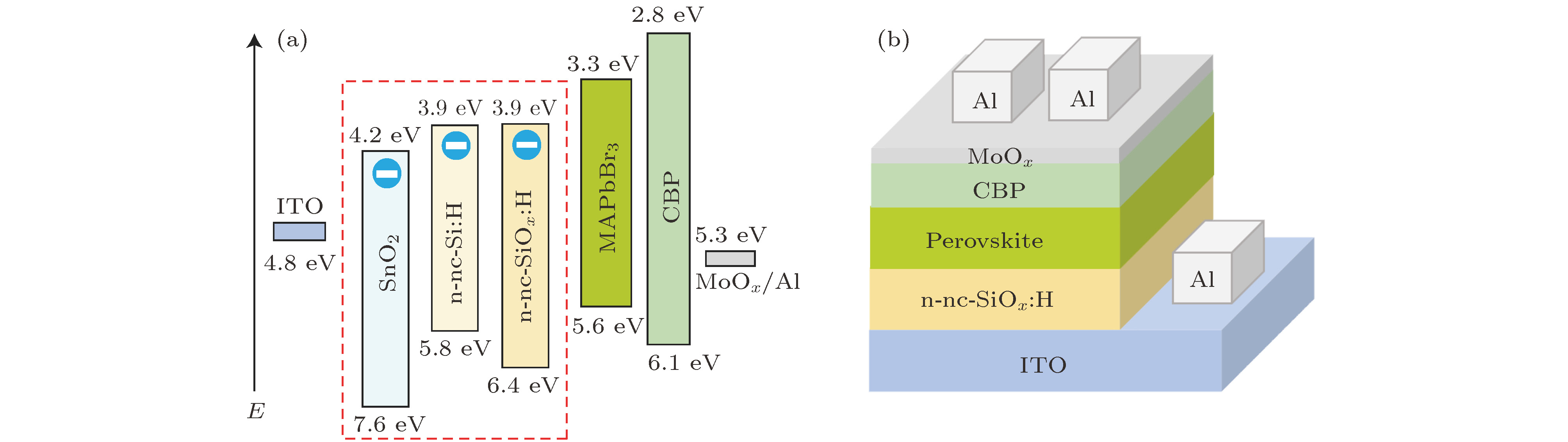
图 1 能级结构与器件结构 (a) PeLEDs器件各层材料的能级结构图; (b) PeLEDs器件结构图
Figure 1. Energy-level diagram and device structure: (a) band alignment of each functional layer; (b) structure diagram of PeLEDs device.

图 2 不同衬底对钙钛矿薄膜的影响 (a)不同衬底表面的原子力显微镜图; (b)不同衬底上生长的钙钛矿薄膜X射线衍射图; (c)不同衬底上生长的钙钛矿薄膜PL光谱图
Figure 2. Influence of different substrates on perovskite films: (a) Atomic force microscopy images of different substrate surfaces; (b) X-ray diffraction patterns of perovskite films on different substrates; (c) photoluminescence spectra of perovskite films on different substrates.
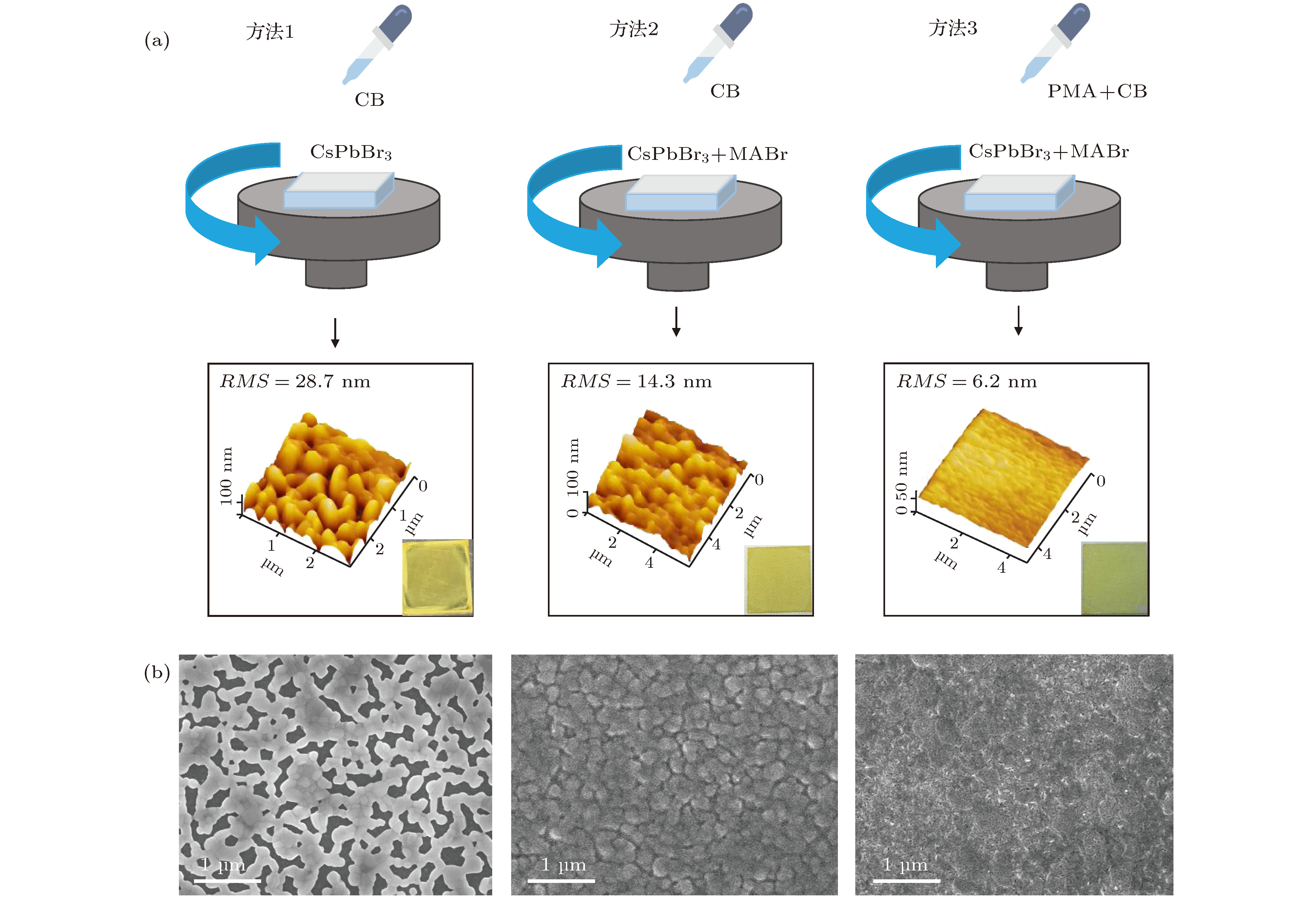
图 3 钙钛矿成膜工艺 (a)三种钙钛矿薄膜制备工艺及对应的原子力显微镜图和实物图; (b)三种工艺下钙钛矿薄膜表面的扫描电子显微镜图
Figure 3. Synthesis of perovskite film: (a) Different fabrication processes of perovskite films and the corresponding atomic force microscopy images and photographs; (b) planar scanning electron microscopy images of the perovskite films based on different fabrication processes.
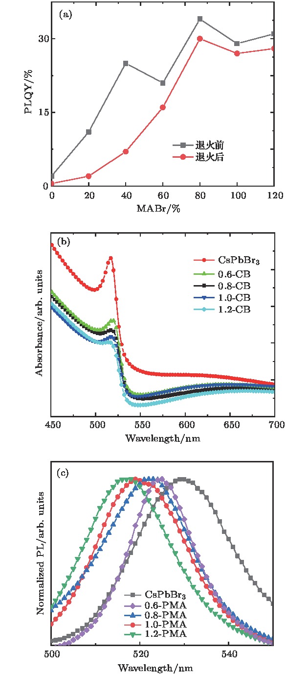
图 4 钙钛矿薄膜的光学性能表征 (a)不同浓度的MABr下, 退火前后钙钛矿薄膜的PLQY变化; (b)钙钛矿薄膜的吸收度; (c)归一化的PL谱
Figure 4. Optical characterization of perovskite films: (a) PLQY of perovskite films before and after annealing at different concentrations of MABr; (b) absorbance spectra of perovskite films; (c) normalized PL spectra of perovskite films.
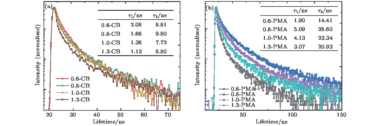
图 5 钙钛矿薄膜在n-nc-SiOx:H基底下的TRPL图 (a)不加PMA时, 不同MABr浓度下钙钛矿TRPL图; (b)加入PMA时, 不同MABr浓度下钙钛矿TRPL图
Figure 5. TRPL spectra of perovskite films on n-nc-SiOx:H: (a) TRPL spectra of perovskite films at different MABr concentrations without PMA additive; (b) TRPL spectra of perovskite films at different MABr concentrations with PMA additive.
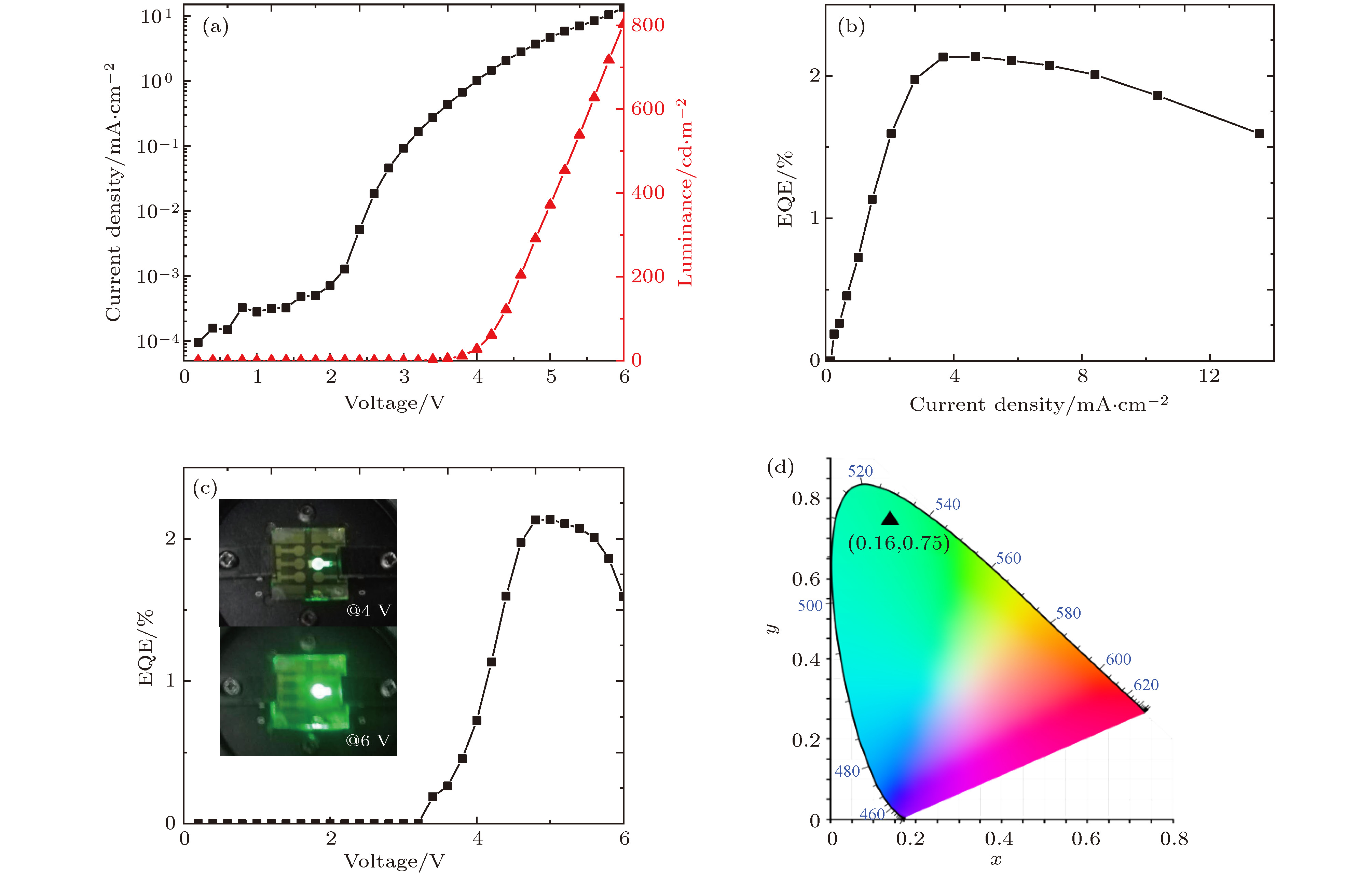
图 6 PeLEDs的电致发光表现 (a)器件的电流密度、光强随电压的变化; (b)器件的EQE随电流密度的变化; (c)器件的EQE随电压的变化; (d)器件发光对应的CIE坐标
Figure 6. Electroluminescence of PeLEDs: (a) Current density and luminance of the device as a function of voltage; (b) EQE of the device as a function of current density; (c) EQE of the device as a function of voltage; (d) the corresponding CIE coordinate.
表 1 基于两种不同电子注入层的PeLEDs器件性能的比较
Table 1. Performance of PeLEDs based on different electron injection layers.
电子注入层 Lmax/cd·m–2 CE/cd·A–1 EQE/% n-nc-Si:H 650 0.4 0.1 n-nc-SiOx:H 2100 1.37 0.43  DownLoad: CSV
-
[1] Kojima A, Teshima K, Shirai Y, Miyasaka T 2009 J. Am. Chem. Soc. 131 6050
Google Scholar
[2] Stranks S D, Eperon G E, Grancini G, Menelaou C, Alcocer M J, Leijtens T, Herz L M, Petrozza A, Snaith H J 2013 Science 342 341
Google Scholar
[3] Jeon N J, Noh J H, Yang W S, Kim Y C, Ryu S, Seo J, Seok S I 2015 Nature 517 476
Google Scholar
[4] Tan H, Jain A, Voznyy O, Lan X, DeArquer F P G, Fan J Z, Bermudez R Q, Yuan M, Zhang B, Zhao Y, Fan F, Li P, Quan L N, Zhao Y, Lu Z, Yang Z, Hoogland S, Sargent E H 2017 Science 355 722
Google Scholar
[5] 姚鑫, 丁艳丽, 张晓丹, 赵颖 2015 物理学报 64 038805
Google Scholar
Yao X, Ding Y L, Zhang X D, Zhao Y 2015 Acta Phys. Sin. 64 038805
Google Scholar
[6] Protesescu L, Yakunin S, Bodnarchuk M I, Krieg F, Caputo R, Hendon C H, Yang R X, Walsh A, Kovalenko M V 2015 Nano Lett. 15 3692
Google Scholar
[7] Chondroudis K, Mitzi D B 1999 Chem. Mater. 11 3028
Google Scholar
[8] Tan Z K, Moghaddam R S, Lai M L, Docampo P, Higler R, Deschler F, Price M, Sadhanala A, Pazos L M, Credgington D, Hanusch F, Bein T, Snaith H J, Friend R H 2014 Nat. Nanotechnol. 9 687
Google Scholar
[9] Song J, Li J, Xu L, Li J, Zhang F, Han B, Shan Q, Zeng H 2018 Adv. Mater. 30 1800764
Google Scholar
[10] Xiao Z, Kerner R A, Zhao L, Tran N L, Lee K M, Koh T W, Scholes G D, Rand B P 2017 Nat. Photon. 11 108
Google Scholar
[11] Yang X, Zhang X, Deng J, Chu Z, Jiang Q, Meng J, Wang P, Zhang L, Yin Z, You J 2018 Nat. Commun. 9 570
Google Scholar
[12] Lu M, Zhang X, Bai X, Wu H, Shen X, Zhang Y, Zhang W, Zheng W, Song H, Yu W W, Rogach A L 2018 ACS Energy Lett. 3 1571
Google Scholar
[13] Chiba T, Hoshi K, Pu Y J, Takeda Y, Hayashi Y, Ohisa S, Kawata S, Kido J 2017 ACS Appl. Mater. Interfaces 9 18054
Google Scholar
[14] Lee J W, Choi Y J, Yang J M, Ham S, Jeon S K, Lee J Y, Song Y H, Ji E K, Yoon D H, Seo S, Shin H, Han G S, Jung H S, Kim D, Park N G 2017 ACS Nano 11 3311
Google Scholar
[15] Yu J C, Kim D B, Baek G, Lee B R, Jung E D, Lee S, Chu J H, Lee D K, Choi K J, Cho S, Song M H 2015 Adv. Mater. 27 3492
Google Scholar
[16] Wang J, Wang N, Jin Y, Si J, Tan Z K, Du H, Cheng L, Dai X, Bai S, He H, Ye Z, Lai M L, Friend R H, Huang W 2015 Adv. Mater. 27 2311
Google Scholar
[17] Zhou Y, Fuentes-Hernandez C, Shim J, Meyer J, Giordano A J, Li H, Winget P, Papadopoulos T, Cheun H, Kim J, Fenoll M, Dindar A, Haske W, Najafabadi E, Khan T M, Sojoudi H, Barlow S, Graham S, Bredas J L, Marder S R, Kahn A, Kippelen B 2012 Science 336 327
Google Scholar
[18] Wang N, Cheng L, Si J, Jin Y, Wang J, Huang W 2016 Appl. Phys. Lett. 108 141102
Google Scholar
[19] Shi Z, Li Y, Zhang Y, Chen Y, Li X, Wu D, Xu T, Shan C, Du G 2017 Nano Lett. 17 313
[20] Zhang L, Yang X, Jiang Q, Wang P, Yin Z, Zhang X, Tan H, Yang Y M, Wei M, Sutherland B R, Sargent E H, You J 2017 Nat. Commun. 8 15640
Google Scholar
[21] Chiba T, Hayashi Y, Ebe H, Hoshi K, Sato J, Sato S, Pu Y J, Ohisa S, Kido J 2018 Nat. Photon. 12 681
Google Scholar
[22] Saliba M, Matsui T, Domanski K, Seo J Y, Ummadisingu A, Zakeeruddin S M, Correa-Baena J P, Tress W R, Abate A, Hagfeldt A, Grätzel M 2016 Science 354 206
Google Scholar
[23] Zou Y, Ban M, Yang Y, Bai S, Wu C, Han Y, Wu T, Tan Y, Huang Q, Gao X, Song T, Zhang Q, Sun B 2018 ACS Appl. Mater. Interfaces 10 24320
Google Scholar
[24] 丁雄傑, 倪露, 马圣博, 马英壮, 肖立新, 陈志坚 2015 物理学报 64 038802
Google Scholar
Ding X J, Ni L, Ma S B, Ma Y Z, Xiao L X, Chen Z J 2015 Acta Phys. Sin. 64 038802
Google Scholar
[25] Yang J, Siempelkamp B D, Mosconi E, de Angelis F, Kelly T 2015 Chem. Mater. 27 4229
Google Scholar
[26] Savenije T J, Huijser A, Vermeulen M J, Katoh R 2008 Chem. Phys. Lett. 461 93
Google Scholar
[27] Jiang Q, Zhang L, Wang H, Yang X, Meng J, Liu H, Yin Z, Wu J, Zhang X, You J 2016 Nat. Energy 2 16177
[28] Simmons J G 1965 Phys. Rev. Lett. 15 967
Google Scholar
[29] Wu I W, Chen Y H, Wang P S, Wang C G, Hsu S H, Wu C I 2010 Appl. Phys. Lett. 96 013301
Google Scholar
[30] Ma D H, Zhang W J, Jiang Z Y, Ma Q, Ma X B, Fan Z Q, Song D Y, Zhang L 2017 Sol. Energy 144 808
Google Scholar
[31] Ren Q, Li S, Zhu S, Ren H, Yao X, Wei C, Yan B, Zhao Y, Zhao X 2018 Sol. Energy Mater. Sol. Cells 185 124
Google Scholar
[32] Stoumpos C C, Malliakas C D, Peters J A, Liu Z, Sebastian M, Im J, Chasapis T C, Wibowo A C, Chung D Y, Freeman A J, Wessels B W, Kanatzidis M G 2013 Cryst. Growth Des. 13 2722
Google Scholar
[33] Lee S, Park J H, Nam Y S, Lee B R, Zhao B, Nuzzo D D, Jung E D, Jeon H, Kim J Y, Jeong H Y, Friend R H, Song M H 2018 ACS Nano 12 3417
Google Scholar
[34] Zhao L, Lee K M, Roh K, Khan S U Z, Rand B P 2019 Adv. Mater. 31 1805836
[35] Shi H, Du M H 2014 Phys. Rev. B 90 174103
Google Scholar
[36] Lin K, Xing J, Quan L N, de Arquer F P G, Gong X, Lu J, Xie L, Zhao W, Zhang D, Yan C, Li W, Liu X, Lu Y, Kirman J, Sargent E H, Xiong Q, Wei Z 2018 Nature 562 245
Google Scholar
[37] Zou W, Li R, Zhang S, Liu Y, Wang N, Cao Y, Miao Y, Xu M, Guo Q, Di D, Zhang L, Yi C, Gao F, Friend R H, Wang J, Huang W 2018 Nat. Commun. 9 608
Google Scholar

 DownLoad:
Catalog
Metrics
- Abstract views: 8683
- PDF Downloads: 109
- Cited By: 0
