


-
As one of the primary elements in magnetoresistive random access memory (MRAM), voltage controlled magnetic anisotropy magnetic tunnel junction (VCMA-MTJ) has received wide attention due to its fast read and write speed, low power dissipation, and compatibility with standard CMOS technology. However, with the downscaling of VCMA-MTJ and the increasing of storage density of MRAM, the effect of process deviation on the characteristics of MTJ becomes more and more obvious, which even leads to Read/Write (R/W) error in VCMA-MTJ circuits. Taking into account the depth deviation of the free layer (γtf) and the depth deviation of the oxide barrier layer (γtox) in magnetron sputtering technique as well as the etching process stability factor (α) caused by the sidewall re-deposition layer in the ion beam etching process, the electrical model of VCMA-MTJ with process deviation is presented in the paper. It is shown that the VCMA-MTJ cannot achieve the effective reversal of the magnetization direction when γtf ≥ 13% and γtox ≥ 11%. The precession of magnetization direction in VCMA-MTJ also becomes instable when α ≤ 0.7. Furthermore, the electrical model of VCMA-MTJ with process deviation is also applied to the R/W circuit to study the effect of process deviation on the R/W error in the circuit. Considering the fact that all of γtf, γtox, and α follow Gauss distribution, The 3σ/μ is adopted to represent the process deviation, with using Monte Carlo simulation, where σ is the standard deviation, and μ is the average value. It is shown that the write error of the circuit goes up to 30 % with 3σ/μ of 0.05 and the voltage (Vb) of 1.15 V. At the same time, the read error of the circuit is 20% with 3σ/μ of 0.05 and driving voltage (Vdd) of 0.6 V. Both the read error rate and the write error rate of the VCMA-MTJ circuit increase as process deviation increases. It is found that the write error rate can be effectively reduced by increasing Vb and reducing the voltage pulse width (tpw). The increasing of Vdd is helpful in reducing the read error rate effectively. Our research presents a useful guideline for designing and analyzing the VCMA-MTJ and VCMA-MTJ read/write circuits.
-
Keywords:
- magnetic tunnel junction /
- voltage controlled magnetic anisotropy /
- process deviation /
- read/write circuits
[1] Ikegawa S, Mancoff F B, Janesky J, Aggarwal S 2020 IEEE Trans. Electron Devices 67 1407
 Google Scholar
[2] Nehra V, Prajapati S, Tankwal P, Zilic Z, Kumar T N, Kaushik B K 2020 IEEE Trans. Magn. 56 1
Google Scholar
[3] Sun Y, Gu J, He W, Wang Q, Jing N, Mao Z, Qian W, Jiang L 2019 IEEE Trans. Circuits Syst. II-Express Briefs 66 753
Google Scholar
[4] Burr G W, Brightsky M J, Sebastian A, Cheng H, Wu J, Kim S, Sosa N E, Papandreou N, Lung H, Pozidis H, Eleftheriou E, Lam C H 2016 IEEE J. Emerg. Sel. Topics Circuits Syst. 6 146
Google Scholar
[5] Wang C Z, Zhang D M, Zhang K L, Zeng L, Wang Y, Hou Z Y, Zhang Y G, Zhao W S 2020 IEEE Trans. Magn. 67 1965
Google Scholar
[6] Ryu J W, Kwon K W 2016 IEEE Trans. Magn. 52 1
Google Scholar
[7] Prajapati S, Kaushik B K 2018 IEEE Trans. Magn. 55 1
Google Scholar
[8] Lee D G, Park S G 2017 IEEE Trans. Magn. 53 1
Google Scholar
[9] Khalili A P, Alzate J G, Cai X Q, Ebrahimi F, Hu Q, Wong K, Wang K L 2015 IEEE Trans. Magn. 51 1
Google Scholar
[10] Zhang X L, Wang C J, Liu Y W, Zhang Z Z, Jin Q Y, Duan C G 2016 Sci. Rep. 6 18719
Google Scholar
[11] Miriyala V P K, Fong X, Liang G 2019 IEEE Trans. Electron Devices. 66 944
Google Scholar
[12] Long M, Zeng L, Gao T, Zhang D, Qin X, Zhang Y, Zhao W 2018 IEEE Trans. Nanotechnol. 17 492
Google Scholar
[13] Song J, Ahmed I, Zhao Z, Zhang D, Sapatnekar S S, Wang J P, Kim C H 2018 IEEE J. Explor. Solid-State Computat. Dev. Circ. 4 76
Google Scholar
[14] Cao K, Li H, Cai W, Wei J, Wang L, Hu Y, Jiang Q, Cui H, Zhao C, Zhao W 2019 IEEE Trans. Magn. 55 1
Google Scholar
[15] Jaiswal A, Agrawal A, Roy K 2018 Sci. Rep. 8 1
Google Scholar
[16] 张楠, 张保, 杨美音, 蔡凯明, 盛宇, 李予才, 邓永城, 王开友 2017 物理学报 66 5
Google Scholar
Zhang N, Zhang B, Yang M Y, Cai K M, Sheng Y, Li Y C, Deng Y C, Wang K Y 2017 Acta Phys. Sin. 66 5
Google Scholar
[17] Kang W, Ran Y, Zhang Y, Lü W, Zhao W 2017 IEEE Trans. Nanotechnol. 16 387
Google Scholar
[18] Lee H, Lee A, Wang S, Ebrahimi F, Gupta P, Amiri P K, Wang K L 2018 IEEE Trans. Magn. 54 1
Google Scholar
[19] Alzate J G, Amiri P K, Upadhyaya P, Cherepov S S, Zhu J, Lewis M, Dorrance R, Katine J A, Langer J, Galatsis K 2012 2012 International Electron Devices Meeting San Francisco, US, December 10–13, 2012 p51
[20] Niranjan M K, Duan C G, Jaswal S S, Tsymbal E Y 2010 Appl. Phys. Lett. 96 222504
Google Scholar
[21] Gilbert T L 2004 IEEE Trans. Magn. 40 3443
Google Scholar
[22] Ahmed R, Victora R H 2018 Appl. Phys. Lett. 112 182401
Google Scholar
[23] Alzate Vinasco J G 2014 Ph. D. Dissertation (California: University of California, Los Angeles
[24] Tsunekawa K, Nagamine Y, Maehara H, Djayaprawira D D, Watanabe N 2007 2006 IEEE International Magnetics Conference San Diego, US, May 8–12, 2006 p855
[25] Rata A D, Braak H, Bürgler D E, Schneider C M 2007 Appl. Phys. Lett. 90 162512
Google Scholar
[26] Zhao W, Zhao X, Zhang B, Cao K, Wang L, Kang W, Shi Q, Wang M, Zhang Y, Wang Y 2016 Materials 9 41
Google Scholar
[27] Wang Y, Cai H, Naviner L A B, Zhao X X, Zhang Y, Slimani M, Klein J O, Zhao W S 2016 Microelectron. Reliab. 64 26
Google Scholar
[28] Ikeda S, Miura K, Yamamoto H, Mizunuma K, Gan H D, Endo M, Kanai S, Hayakawa J, Matsukura F, Ohno H 2010 Nat. Mater. 9 721
Google Scholar
[29] Chen E, Schwarz B, Choi C J, Kula W, Wolfman J, Ounadjela K, Geha S 2003 J. Appl. Phys. 93 8379
Google Scholar
[30] Ohsawa Y, Shimomura N, Daibou T, Kamiguchi Y, Shirotori S, Inokuchi T, Saida D, Altansargai B, Kato Y, Yoda H 2016 IEEE Trans. Magn. 52 1
Google Scholar
[31] Ip V, Huang S, Carnevale S D, Berry I L, Rook K, Lill T B, Paranjpe A P, Cerio F 2017 IEEE Trans. Magn. 53 1
Google Scholar
[32] Sugiura K, Takahashi S, Amano M, Kajiyama T, Iwayama M, Asao Y, Shimomura N, Kishi T, Ikegawa S, Yoda H 2009 Jpn. J. Appl. Phys. 48 08HD02
Google Scholar
[33] Takahashi S, Kai T, Shimomura N, Ueda T, Amano M, Yoshikawa M, Kitagawa E, Asao Y, Ikegawa S, Kishi T 2006 IEEE Trans. Magn. 42 2745
Google Scholar
[34] Xue L, Nistor L, Ahn J, Germain J, Ching C, Balseanu M, Trinh C, Chen H, Hassan S, Pakala M 2014 IEEE Trans. Magn. 50 1
Google Scholar
[35] Wang Y, Zhang Y, Deng E Y, Klein J O, Naviner L A B, Zhao W S 2014 Microelectron. Reliab. 54 1774
Google Scholar
[36] Aggarwal S, Almasi H, DeHerrera M, Hughes B, Ikegawa S, Janesky J, Lee H K, Lu H, Mancoff F B, Nagel K, Shimon G, Sun J J, Andre T, Alam S M 2019 2019 IEEE International Electron Devices Meeting (IEDM) San Francisco, USA, December 7–11, 2019 p18
[37] Li J, Augustine C, Salahuddin S, Roy K 2008 Proceedings of the 45th annual Design Automation Conference New York, USA, June, 2008 p278
-

图 1 VCMA-MTJ结构示意图
Figure 1. Schematic structure of the VCMA-MTJ device.
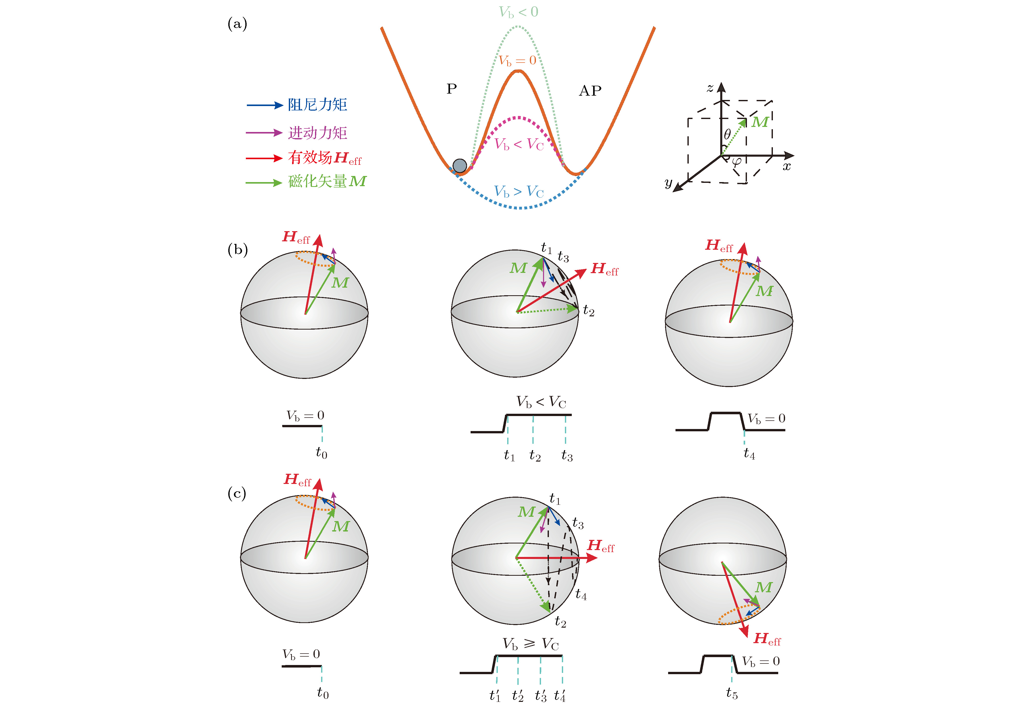
图 2 VCMA-MTJ的磁化动力学示意图 (a)不同电压对MTJ磁化状态能量势垒的影响; (b)Vb < VC的情况; (c)Vb > VC的情况
Figure 2. Illustration of magnetization dynamics for the VCMA-MTJ device: (a) The impacts of different voltages on the energy barrier of MTJ; (b) at a relatively low voltage (Vb < VC); (c) at a high positive voltage (Vb > VC).

图 3 VCMA-MTJ磁化状态随时间的变化曲线, 其中插图是切换速度的定义
Figure 3. Magnetization state versus time of VCMA-MTJ, the inset represents the definition of the switching speed.
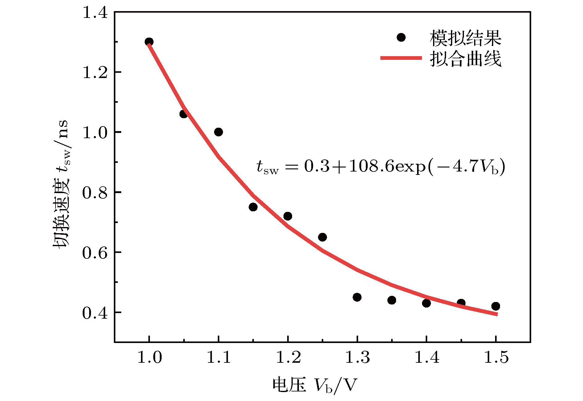
图 4 不同Vb对VCMA-MTJ磁化状态切换速度的影响, 其中tpw = 0.4 ns
Figure 4. Effect of Vb on the magnetization direction switching speed of VCMA-MTJ at tpw = 0.4 ns.

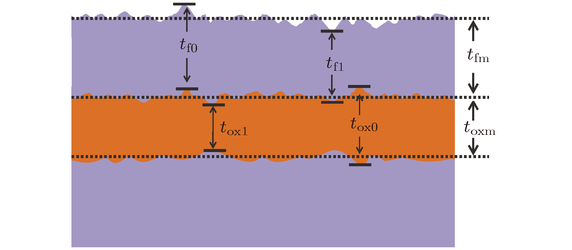
图 6 薄膜生长工艺产生的厚度偏差示意图
Figure 6. Schematic illustration of thickness deviation caused by the thin film growth process.
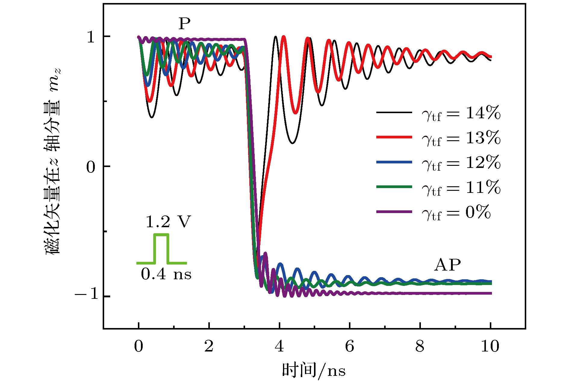
图 7 γtf对VCMA-MTJ磁化方向切换的影响, 其中Vb = 1.2 V, tpw = 0.4 ns
Figure 7. Effect of γtf on the magnetization direction switchingof VCMA-MTJ at Vb = 1.2 V, tpw = 0.4 ns.
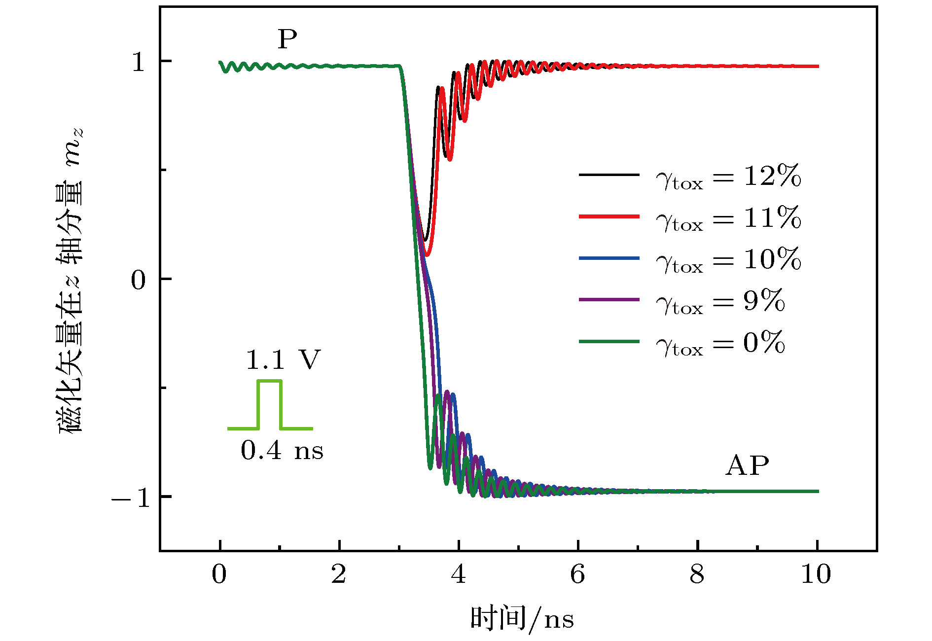
图 8 不同γtox对VCMA-MTJ磁化状态切换的影响, 其中Vb = 1.1 V, tpw = 0.4 ns
Figure 8. Effect of γtox on magnetization direction switching of VCMA-MTJ at Vb = 1.1 V and tpw = 0.4 ns.
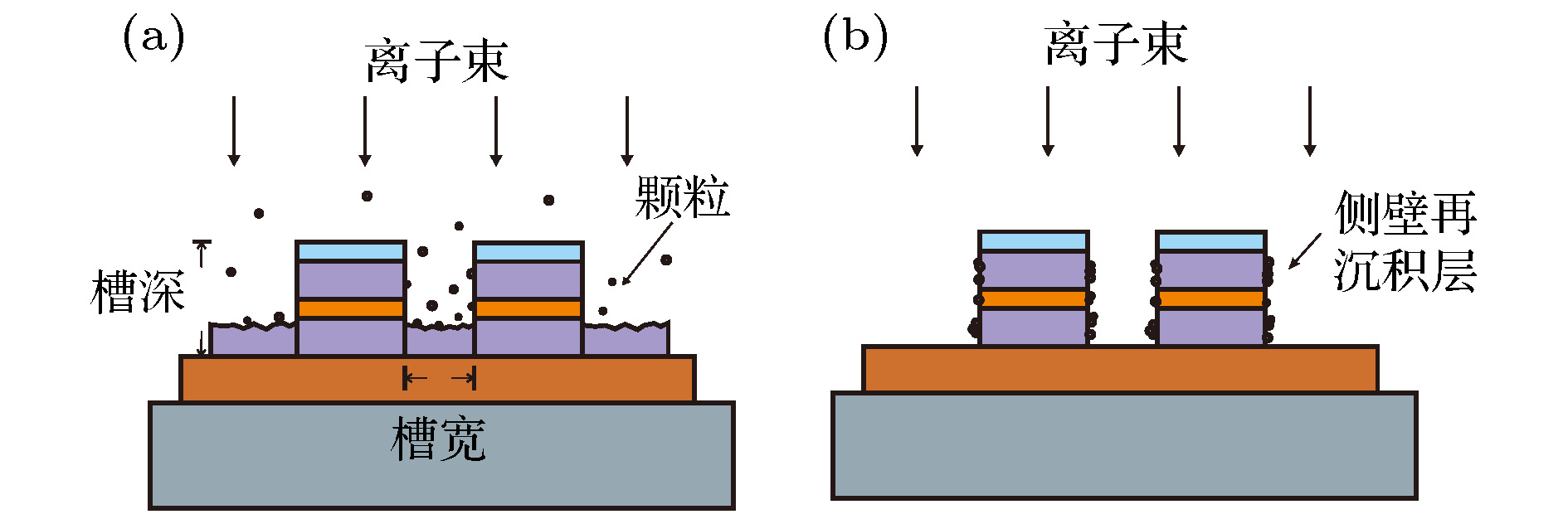
图 9 离子束刻蚀产生侧壁再沉积层示意图 (a)刻蚀产生磁性粒子; (b)粒子聚集形成再沉积层
Figure 9. Illustration of the formation of the sidewall re-deposited layer with ion beam etching: (a) Producing of magnetic particleses with etching process; (b) formation of the re-deposition layer with magnetic particleses.
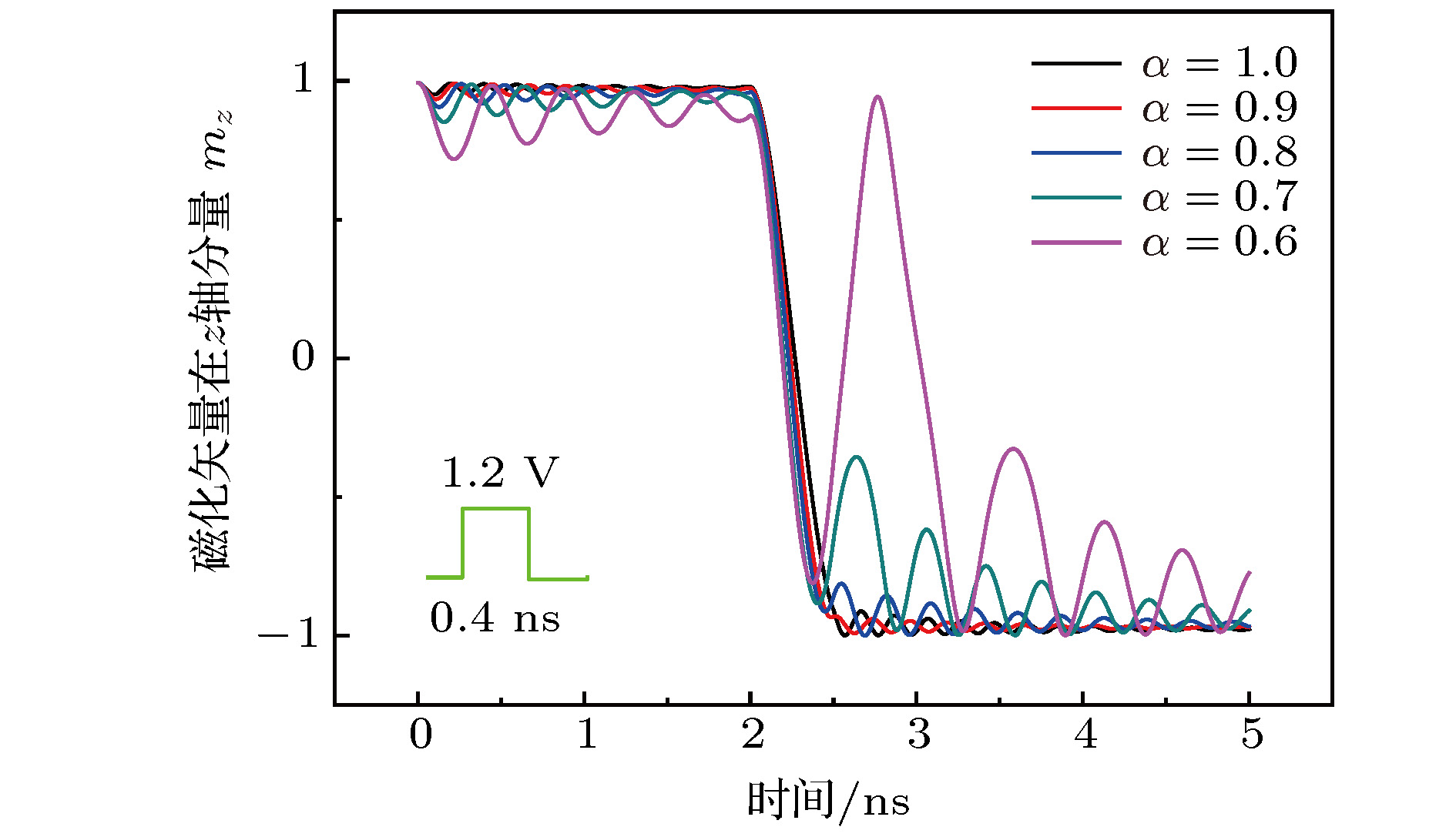
图 10 不同α对VCMA-MTJ磁化方向切换的影响
Figure 10. Effect of α on magnetization direction switching of VCMA-MTJ.
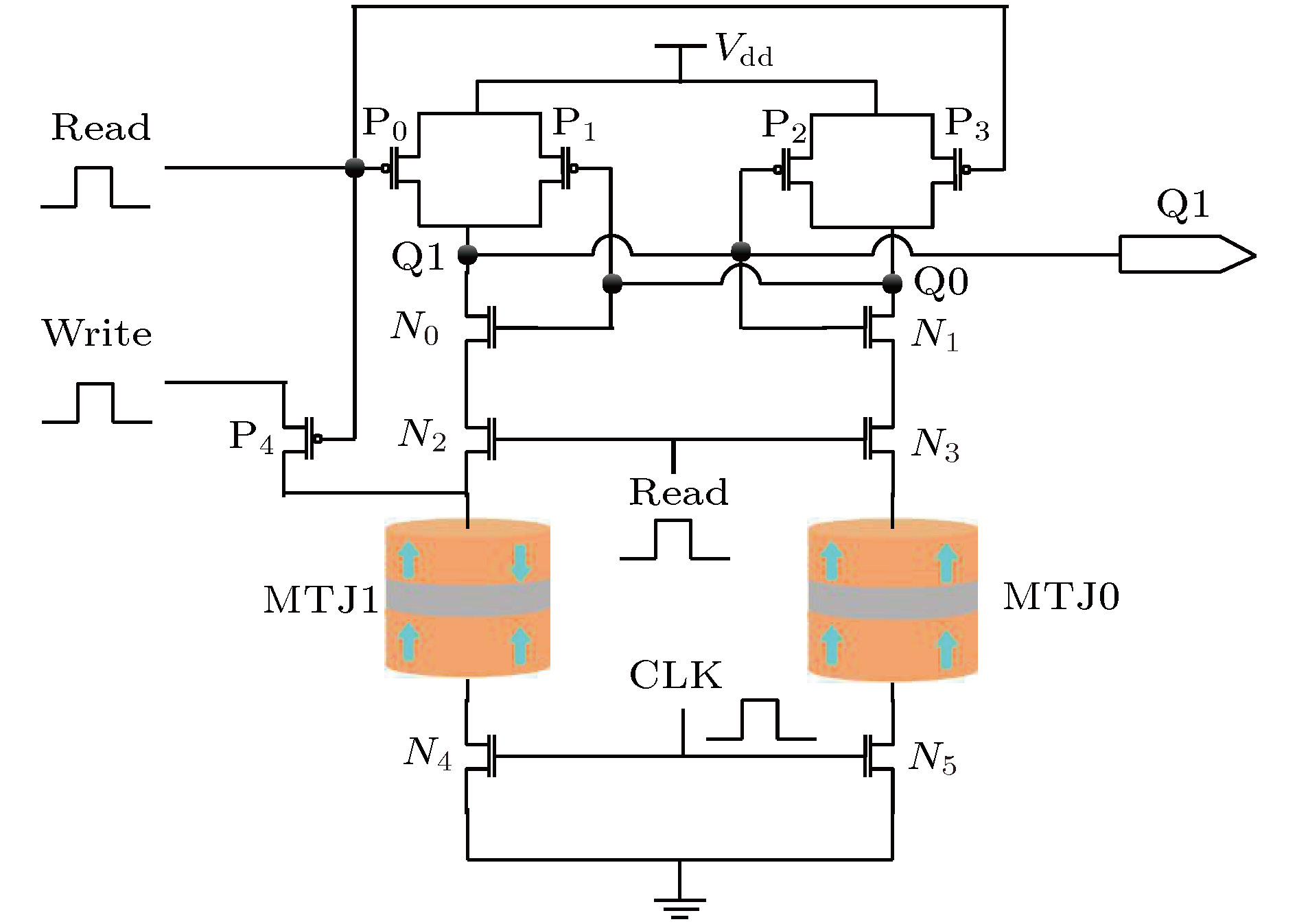
图 11 VCMA-MTJ读写电路
Figure 11. Reading and writing circuit of VCMA-MTJ.

图 12 VCMA-MTJ读写电路的仿真波形
Figure 12. Simulation waveform of the reading and writing circuit of VCMA-MTJ.
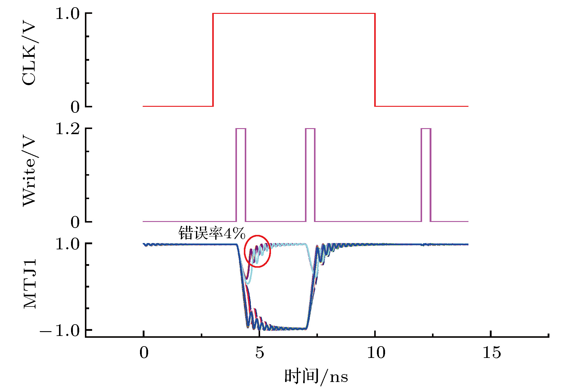
图 13 VCMA-MTJ写电路的蒙特卡洛仿真波形, 其中N = 100, 3σ/μ = 0.03, Vb = 1.2 V, tpw = 0.4 ns
Figure 13. Monte Carlo simulation waveform of the writing circuit of VCMA-MTJ at N = 100, 3σ/μ = 0.03, Vb = 1.2 V, tpw = 0.4 ns.
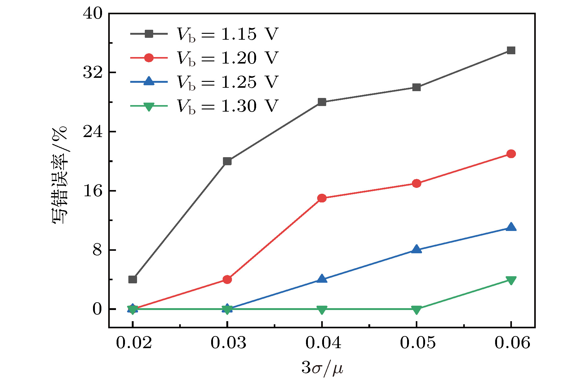
图 14 不同Vb下写错误率随3σ/μ的变化关系
Figure 14. Writing error rate versus 3σ/μ at different Vb
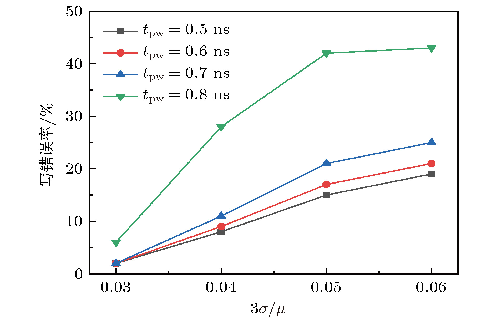
图 15 不同tpw下写错误率随3σ/μ的变化关系
Figure 15. Writing error rate versus 3σ/μ at different tpw.

图 16 VCMA-MTJ读电路的蒙特卡洛仿真波形, 其中N = 100, 3σ/μ = 0.07, Vdd = 0.8 V
Figure 16. Monte Carlo simulation waveform of the reading circuit of VCMA-MTJ at N = 100, 3σ/μ = 0.07, Vdd = 0.8 V
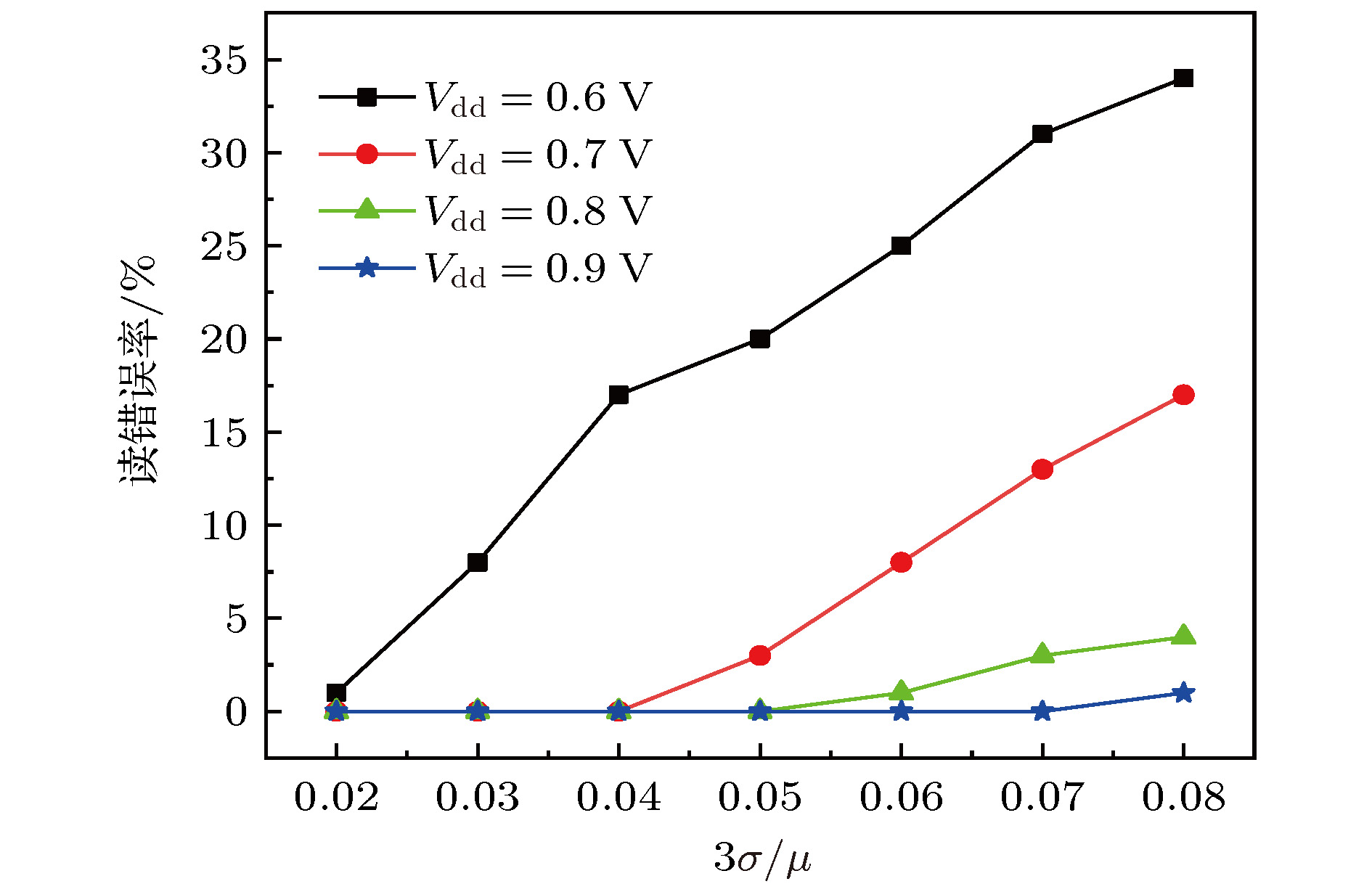
图 17 不同Vdd下读错误率随3σ/μ的变化关系
Figure 17. Reading error rate versus 3σ/μ at different Vdd.
表 1 VCMA-MTJ模型参数列表
Table 1. Parameters of the VCMA-MTJ model.
参数 符号 数值 单位 氧化势垒层厚度标准值 tox 1.4 nm 垂直磁各向异性系数 Ki 0.32 mJ/m2 电压调控磁各项异性系数 ξ 60 fJ/(V·m) 自由层厚度标准值 tf 1.1 nm 简化的旋磁比 γ 2.21 × 10⁵ m/(A·s) 磁导率 μ0 1.256 × 10⁻⁶ H/m 吉尔伯特阻尼因子 αd 0.05 饱和磁化强度 Ms 0.625 × 10⁶ A/m x, y 轴退磁因子 Nx, y 0.0168 z 轴退磁因子 Nz 0.966 外加磁场在 x 轴分量 Hx 31830 A/m  DownLoad: CSV
-
[1] Ikegawa S, Mancoff F B, Janesky J, Aggarwal S 2020 IEEE Trans. Electron Devices 67 1407
Google Scholar
[2] Nehra V, Prajapati S, Tankwal P, Zilic Z, Kumar T N, Kaushik B K 2020 IEEE Trans. Magn. 56 1
Google Scholar
[3] Sun Y, Gu J, He W, Wang Q, Jing N, Mao Z, Qian W, Jiang L 2019 IEEE Trans. Circuits Syst. II-Express Briefs 66 753
Google Scholar
[4] Burr G W, Brightsky M J, Sebastian A, Cheng H, Wu J, Kim S, Sosa N E, Papandreou N, Lung H, Pozidis H, Eleftheriou E, Lam C H 2016 IEEE J. Emerg. Sel. Topics Circuits Syst. 6 146
Google Scholar
[5] Wang C Z, Zhang D M, Zhang K L, Zeng L, Wang Y, Hou Z Y, Zhang Y G, Zhao W S 2020 IEEE Trans. Magn. 67 1965
Google Scholar
[6] Ryu J W, Kwon K W 2016 IEEE Trans. Magn. 52 1
Google Scholar
[7] Prajapati S, Kaushik B K 2018 IEEE Trans. Magn. 55 1
Google Scholar
[8] Lee D G, Park S G 2017 IEEE Trans. Magn. 53 1
Google Scholar
[9] Khalili A P, Alzate J G, Cai X Q, Ebrahimi F, Hu Q, Wong K, Wang K L 2015 IEEE Trans. Magn. 51 1
Google Scholar
[10] Zhang X L, Wang C J, Liu Y W, Zhang Z Z, Jin Q Y, Duan C G 2016 Sci. Rep. 6 18719
Google Scholar
[11] Miriyala V P K, Fong X, Liang G 2019 IEEE Trans. Electron Devices. 66 944
Google Scholar
[12] Long M, Zeng L, Gao T, Zhang D, Qin X, Zhang Y, Zhao W 2018 IEEE Trans. Nanotechnol. 17 492
Google Scholar
[13] Song J, Ahmed I, Zhao Z, Zhang D, Sapatnekar S S, Wang J P, Kim C H 2018 IEEE J. Explor. Solid-State Computat. Dev. Circ. 4 76
Google Scholar
[14] Cao K, Li H, Cai W, Wei J, Wang L, Hu Y, Jiang Q, Cui H, Zhao C, Zhao W 2019 IEEE Trans. Magn. 55 1
Google Scholar
[15] Jaiswal A, Agrawal A, Roy K 2018 Sci. Rep. 8 1
Google Scholar
[16] 张楠, 张保, 杨美音, 蔡凯明, 盛宇, 李予才, 邓永城, 王开友 2017 物理学报 66 5
Google Scholar
Zhang N, Zhang B, Yang M Y, Cai K M, Sheng Y, Li Y C, Deng Y C, Wang K Y 2017 Acta Phys. Sin. 66 5
Google Scholar
[17] Kang W, Ran Y, Zhang Y, Lü W, Zhao W 2017 IEEE Trans. Nanotechnol. 16 387
Google Scholar
[18] Lee H, Lee A, Wang S, Ebrahimi F, Gupta P, Amiri P K, Wang K L 2018 IEEE Trans. Magn. 54 1
Google Scholar
[19] Alzate J G, Amiri P K, Upadhyaya P, Cherepov S S, Zhu J, Lewis M, Dorrance R, Katine J A, Langer J, Galatsis K 2012 2012 International Electron Devices Meeting San Francisco, US, December 10–13, 2012 p51
[20] Niranjan M K, Duan C G, Jaswal S S, Tsymbal E Y 2010 Appl. Phys. Lett. 96 222504
Google Scholar
[21] Gilbert T L 2004 IEEE Trans. Magn. 40 3443
Google Scholar
[22] Ahmed R, Victora R H 2018 Appl. Phys. Lett. 112 182401
Google Scholar
[23] Alzate Vinasco J G 2014 Ph. D. Dissertation (California: University of California, Los Angeles
[24] Tsunekawa K, Nagamine Y, Maehara H, Djayaprawira D D, Watanabe N 2007 2006 IEEE International Magnetics Conference San Diego, US, May 8–12, 2006 p855
[25] Rata A D, Braak H, Bürgler D E, Schneider C M 2007 Appl. Phys. Lett. 90 162512
Google Scholar
[26] Zhao W, Zhao X, Zhang B, Cao K, Wang L, Kang W, Shi Q, Wang M, Zhang Y, Wang Y 2016 Materials 9 41
Google Scholar
[27] Wang Y, Cai H, Naviner L A B, Zhao X X, Zhang Y, Slimani M, Klein J O, Zhao W S 2016 Microelectron. Reliab. 64 26
Google Scholar
[28] Ikeda S, Miura K, Yamamoto H, Mizunuma K, Gan H D, Endo M, Kanai S, Hayakawa J, Matsukura F, Ohno H 2010 Nat. Mater. 9 721
Google Scholar
[29] Chen E, Schwarz B, Choi C J, Kula W, Wolfman J, Ounadjela K, Geha S 2003 J. Appl. Phys. 93 8379
Google Scholar
[30] Ohsawa Y, Shimomura N, Daibou T, Kamiguchi Y, Shirotori S, Inokuchi T, Saida D, Altansargai B, Kato Y, Yoda H 2016 IEEE Trans. Magn. 52 1
Google Scholar
[31] Ip V, Huang S, Carnevale S D, Berry I L, Rook K, Lill T B, Paranjpe A P, Cerio F 2017 IEEE Trans. Magn. 53 1
Google Scholar
[32] Sugiura K, Takahashi S, Amano M, Kajiyama T, Iwayama M, Asao Y, Shimomura N, Kishi T, Ikegawa S, Yoda H 2009 Jpn. J. Appl. Phys. 48 08HD02
Google Scholar
[33] Takahashi S, Kai T, Shimomura N, Ueda T, Amano M, Yoshikawa M, Kitagawa E, Asao Y, Ikegawa S, Kishi T 2006 IEEE Trans. Magn. 42 2745
Google Scholar
[34] Xue L, Nistor L, Ahn J, Germain J, Ching C, Balseanu M, Trinh C, Chen H, Hassan S, Pakala M 2014 IEEE Trans. Magn. 50 1
Google Scholar
[35] Wang Y, Zhang Y, Deng E Y, Klein J O, Naviner L A B, Zhao W S 2014 Microelectron. Reliab. 54 1774
Google Scholar
[36] Aggarwal S, Almasi H, DeHerrera M, Hughes B, Ikegawa S, Janesky J, Lee H K, Lu H, Mancoff F B, Nagel K, Shimon G, Sun J J, Andre T, Alam S M 2019 2019 IEEE International Electron Devices Meeting (IEDM) San Francisco, USA, December 7–11, 2019 p18
[37] Li J, Augustine C, Salahuddin S, Roy K 2008 Proceedings of the 45th annual Design Automation Conference New York, USA, June, 2008 p278

 DownLoad:
Catalog
Metrics
- Abstract views: 6580
- PDF Downloads: 118
- Cited By: 0
