


-
In the case of methylammonium lead halide (MAPbH3) perovskite solar cells, the indium tin oxide (ITO) film has been widely used as the transparent electrode. In the preparation process and service process of MAPbH3 perovskite solar cells, the MAPbH3 perovskite layer can decompose into the methyl, amino, methylammonium, halide ion/group, etc. Thus, the diffusion of ammonia ion/group into ITO film is inevitable, which can seriously deteriorate the electrical property of ITO transparent electrode. In this study, the ITO films with and without (100) preferred orientation are bombarded by a low-energy ammonia (NHx) ion beam. After the bombardment, the electrical properties of ITO film without preferred orientation are deteriorated seriously, especially for carrier concentration, which is deteriorated down to an extent of about 5–6 orders of magnitude. The bombardment of low-energy NHx ion/group has little influence on the electrical properties of ITO film with (100) preferred orientation. Such phenomena can be explained by the following reasons. Based on XPS measurement results, the low-energy NHx ion/group diffuses into the ITO film surface after the bombardment. In the diffusion process, the low-energy NHx ion/group is mainly bonded with O in ITO lattice, which results in the formation of In/Sn—O—N bond. Based on the crystal structure of ITO, the (100) lattice of ITO consists of In/Sn, and the calculated value of surface energy
$ {\gamma }_{\left\{100\right\}/\left\{010\right\}/\left\{001\right\}} $ = 1.76 J/m2. While the (110) and (111) lattices of ITO consist of In/Sn/O, in which the O atom percent on (110) and (111) lattices are 56 at.% and 25 at.% respectively. Besides, the calculated values of surface energy$ {\gamma }_{\left\{110\right\}/\left\{101\right\}/\left\{011\right\}} $ and$ {\gamma }_{\left\{111\right\}} $ are 1.07 and 0.89 J/m2, respectively. Combining the XPS measurement results and crystal structure of ITO, it can be understood that in the diffusion process of low-energy NHx ion/group into ITO film without preferred orientation, lots of In/Sn—O—N bonds are formed in the ITO lattices, which are rich in O and have lower surface energy$ \gamma $ . Then, after the low-energy NHx ion/group bombardment, the electrical properties of ITO film without preferred orientation are deteriorated seriously. On the contrary, because of the absence of O and the highest surface energy$ \gamma $ , it is hard for the low-energy NHx ion/group to diffuse into ITO (100) lattice. Then, after the low-energy NHx ion/group bombardment, the electrical properties of ITO film with (100) preferred orientation have little change. With all results, the ITO film with (100) preferred orientation can be an ideal candidate for transparent electrode in MAPbH3 perovskite solar cells.-
Keywords:
- indium tin oxide /
- preferred orientation /
- ammonia ion/group /
- electrical property
[1] Kojima A, Teshima K, Shirai Y, Miyasaka T 2009 J. Am. Chem. Soc. 131 6050
 Google Scholar
[2] Lee M M, Teuscher J, Miyasaka T, Murakami T N, Snaith H J 2012 Science 338 643
Google Scholar
[3] Jung E H, Jeon N J, Park E Y, Moon C S, Shin T J, Yang T Y, Noh J H, Seo J 2019 Nature 567 511
Google Scholar
[4] National Renewable Energy Laboratory (NREL), Best research cell efficiencies, https://www.nrel.gov/pv [2020-04-25]
[5] Tan H R, Jain A, Voznyy O, Lan X Z, Arquer de F P G, Fan J Z, Quintero-Bermudez R, Yuan M J, Zhang B, Zhao Y C, Fan F J, Li P C, Quan L N, Zhao Y B, Lu Z H, Yang Z Y, Hoogland S, Sargent E H 2017 Science 355 722
Google Scholar
[6] 王言博, 崔丹钰, 张才益, 韩礼元, 杨旭东 2019 物理学报 68 158401
Google Scholar
Wang Y B, Cui D Y, Zhang C Y, Han L Y, Yang X D 2019 Acta Phys. Sin. 68 158401
Google Scholar
[7] Ono L K, Juarez-Perez E J, Qi Y B 2017 ACS Appl. Mater. Interfaces 9 30197
Google Scholar
[8] Asghar M I, Zhang J, Wang H, Lund P D 2017 Renewable Sustainable Energy Rev. 77 131
Google Scholar
[9] 张钰, 周欢萍 2019 物理学报 68 158804
Google Scholar
Zhang Y, Zhou H P 2019 Acta Phys. Sin. 68 158804
Google Scholar
[10] Zhao S, Lü Z, Guo X, Liu C, Wang H, Jiang W, Liu S, Wang N, Cui Y, Ding W, Han B, Ju D 2018 Materials 11 01991
Google Scholar
[11] Shen L H, Liu J, Lü W, Wu L J, Qi D L, Zhou Y W, Lei W W 2019 Appl. Surf. Sci. 476 418
Google Scholar
[12] Liu H Y, Avrutin V, Izyumskaya N, Ozgur U, Morkoc H 2010 Superlattices Microstruct. 48 458
Google Scholar
[13] Lü Z X, Liu J D, Wang D Y, Tao H L, Chen W C, Sun H T, He Y F, Zhang X, Qu Z Y, Han Z C, Guo X L, Zhao S P, Cui Y X, Wang H L, Liu S M, Liu C Q, Wang N, Jiang W W, Chai W P, Ding W D 2018 Mater. Chem. Phys. 209 38
Google Scholar
[14] Chen W C, Sun H T, Jiang W W, Wang H L, Liu S M, Liu C Q, Wang N, Cui Y X, Chai W P, Ding W Y, Han B 2018 Mater. Lett. 220 8
Google Scholar
[15] Beamson G, Briggs D 1992 High Resolution XPS of Organic Polymers: the Scienta ESCA3000 database (New York: Wiley) pp53−277
[16] Moulder J F, Stickle W F, Sobol P E, Bomben K D 1995 Handbook of X-ray Photoelectron Spectroscopy (Eden Prairie: Physical Electronics Inc.) pp29−198
[17] Barquinha P, Martins R, Pereira L, Fortunato E 2012 Transparent Oxide Electronics: From Materials to Devices (West Sussex: John Wiley & Sons, Ltd.) p12
[18] Levy D, Castellón E 2018 Transparent Conductive Materials: From Materials via Synthesis and Characterization to Applications (Weinheim: Wiley-VCH Verlag GmbH & Co. KGaA) p57
[19] Lee H C, Park O O 2004 Vacuum 75 275
Google Scholar
[20] Mei F, Yuan T, Li R, Qin K, Huang J 2018 J. Mater. Sci.- Mater. Electron. 29 14620
Google Scholar
[21] Lüth H 2015 Solid Surfaces, Interfaces and Thin Films (6th Ed.) (New York: Springer-Verlag) pp271−315
[22] 吴自勤, 王兵, 孙霞 2017 薄膜生长(第二版) (北京: 科学出版社) 第105−124页
Wu Z Q, Wang B, Sun X 2017 The Film Growth (2nd Ed.) (Beijing: Science Press) pp105−124 (in Chinese)
[23] Villars P 1997 Pearson’s Handbook Desk Edition: Crystallographic Data for Intermetallic Phases (Ohio: ASM International) p2195
[24] Zhang S, Dong D D, Wang Z J, Dong C, Häussler P 2018 Sci. China Mater. 61 409
Google Scholar
[25] 蔡昕旸, 王新伟, 张玉苹, 王登魁, 方铉, 房丹, 王晓华, 魏志鹏 2018 物理学报 67 180201
Google Scholar
Cai X Y, Wang X W, Zhang Y P, Wang D K, Fang X, Fang D, Wang X H, Wei Z P 2018 Acta Phys. Sin. 67 180201
Google Scholar
[26] Liu H, Zhang Y, Zhang X, Wang Q, Wang H L, Zhang S, Ma Y P, Cui Y X, Ding W Y, Dong C 2020 J. Alloys Compd. 836 155514
Google Scholar
[27] Kittel C 2005 Introduction to Solid State Physics (8th Ed.) (Hoboken: John Wiley & Sons, Inc.) p374
[28] Hofmann P 2015 Solid State Physics: An Introduction (2nd Ed.) (Weinheim: Wiley-VCH Verlag GmbH & Co. KGaA) p285
[29] Zhang K H L, Walsh A, Catlow C R A, Lazarov V K, Egdell R G 2010 Nano Lett. 10 3740
Google Scholar
[30] 蒋行, 周玉荣, 刘丰珍, 周玉琴 2018 物理学报 67 177802
Google Scholar
Jiang H, Zhou Y R, Liu F Z, Zhou Y Q 2018 Acta Phys. Sin. 67 177802
Google Scholar
[31] Lieberman M A, Lichtenberg A J 2005 Principles of Plasma Discharges and Materials Processing (2nd Ed.) (Hoboken: Wiley-Interscience) pp107−215
[32] 汤玉寅, 王浪平 2012 等离子体浸泡式离子注入与沉积技术 (北京: 国防工业出版社) 第21−54页
Tang Y Y, Wang L P 2012 Plasma Immersion Ion Implantation and Deposition Technique, (Beijing: National Defense Industry Press) pp21−54 (in Chinese)
-
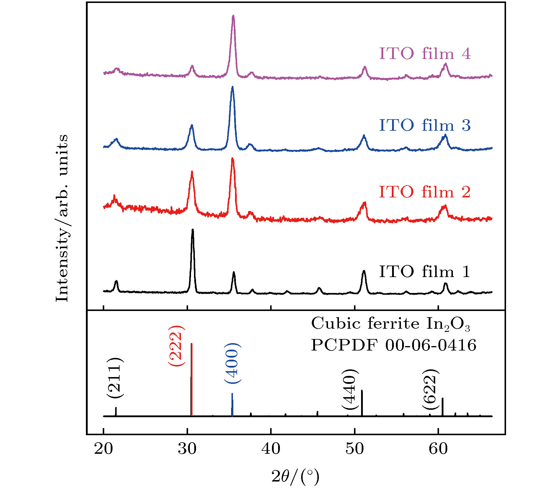
图 1 原始ITO薄膜XRD谱线
Figure 1. XRD patterns of original ITO films.

图 2 与低能NHx离子/基团相互作用前后ITO薄膜的电学性质 (a) 电阻率; (b) 载流子浓度; (c) 载流子迁移率
Figure 2. The electronic property of ITO films before and after low-energy NHx ion/group bombardment: (a) Resistivity; (b) carrier concentration; (c) carrier mobility.

图 3 高分辨XPS谱 (a) ITO薄膜1与低能NHx离子/基团相互作用前的N 1s峰; (b) ITO薄膜1—4与低能NHx离子/基团相互作用后的N 1s峰; (c) ITO薄膜1与低能NHx离子/基团相互作用前的O 1s峰; (d) ITO薄膜1—4与低能NHx离子/基团相互作用后的O 1s峰
Figure 3. High-resolution XPS spectrum: (a) N 1s for ITO film a before low-energy NHx ion/group bombardment; (b) O 1s for ITO film a before low-energy NHx ion/group bombardment; (c) N 1s for ITO films 1 to 4 bombarded by low-energy NHx ion/group; (d) O 1s for ITO films 1 to 4 bombarded by low-energy NHx ion/group.

图 4 ITO薄膜1与低能NHx离子/基团相互作用后O 1s高分辨XPS谱Gaussian拟合结果
Figure 4. Gaussian peak fitting procedure applied to O 1s high-resolution XPS spectrum of ITO film 1 bombarded by low-energy NHx ion/group.

图 5 N元素原子百分比, M—O—N化学键占N 总化学键和O总化学键的百分比
Figure 5. Atomic percentage of N, as well as percentage of M—O—N bond from all N bonds and O bonds, respectively.
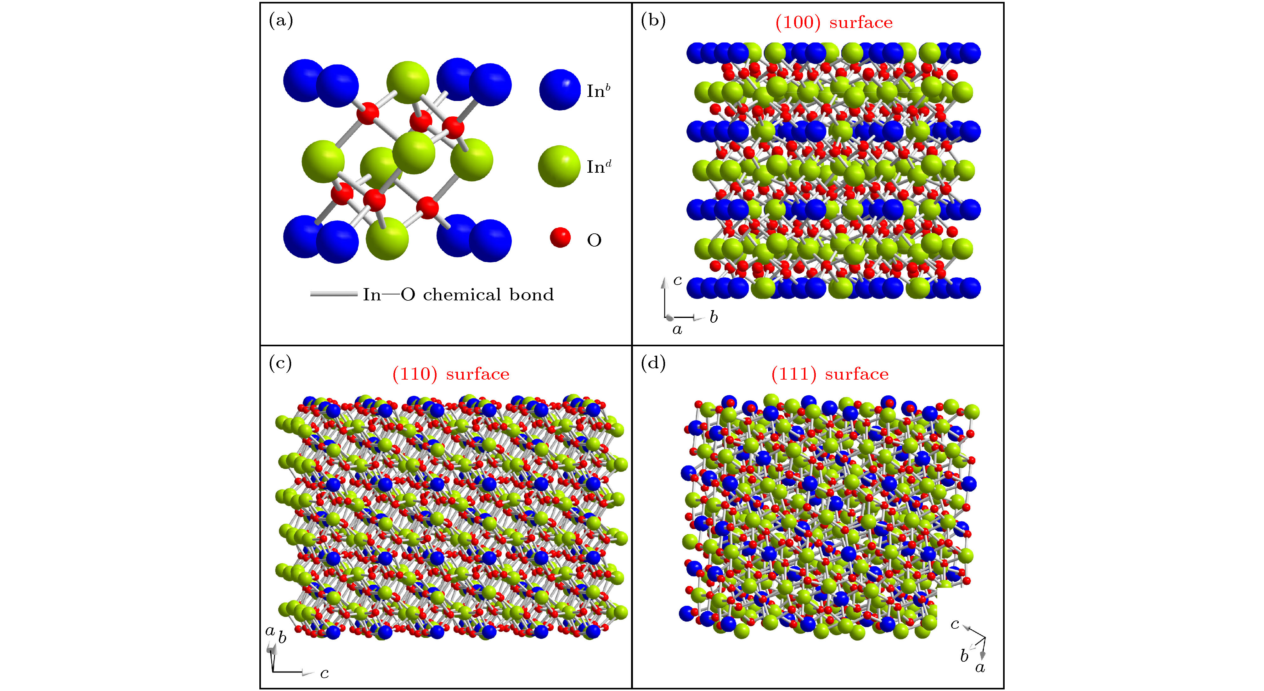
图 6 In2O3晶体结构示意图 (a) In2O3原胞; (b) In2O3 (100)/(010)/(001)晶面; (c) In2O3 (110) (101)/(011)晶面; (d) In2O3 (111)晶面
Figure 6. Schematic illustration of In2O3 unit cell: (a) Primitive unit cell of In2O3; (b) schematic illustration of side view (100) surface; (c) schematic illustration of side view (110) surface; (d) schematic illustration of side view (111) surface.
表 1 ITO薄膜1—4的制备参数
Table 1. The detailed deposition parameters for ITO film 1—4.
沉积参数 数值 Base pressure/Pa 1.0 × 10⁻³ Flow rate of Ar/sccm 20 Distance between target and substrate/cm 12 Pulse frequency/kHz 100 Reverse time/μs 1 Sputtering power density/W·cm–2 2 (Film 1) 4 (Film 2) 6 (Film 3) 8 (Film 4) Working pressure/Pa 0.6  DownLoad: CSV
表 2 ITO薄膜1—4的(222)x系数、(100)x系数和(100)取向比重系数
Table 2. The coefficient of (222)x, (100)x, and (100) lattice plane proportion of ITO film 1–4.
(222)x系数 (100)x系数 (100)取向比重系数 ITO film 1 1.00 1.00 1.00 ITO film 2 0.67 2.78 4.15 ITO film 3 0.41 3.12 7.61 ITO film 4 0.18 3.08 17.11
DownLoad: CSV
-
[1] Kojima A, Teshima K, Shirai Y, Miyasaka T 2009 J. Am. Chem. Soc. 131 6050
Google Scholar
[2] Lee M M, Teuscher J, Miyasaka T, Murakami T N, Snaith H J 2012 Science 338 643
Google Scholar
[3] Jung E H, Jeon N J, Park E Y, Moon C S, Shin T J, Yang T Y, Noh J H, Seo J 2019 Nature 567 511
Google Scholar
[4] National Renewable Energy Laboratory (NREL), Best research cell efficiencies, https://www.nrel.gov/pv [2020-04-25]
[5] Tan H R, Jain A, Voznyy O, Lan X Z, Arquer de F P G, Fan J Z, Quintero-Bermudez R, Yuan M J, Zhang B, Zhao Y C, Fan F J, Li P C, Quan L N, Zhao Y B, Lu Z H, Yang Z Y, Hoogland S, Sargent E H 2017 Science 355 722
Google Scholar
[6] 王言博, 崔丹钰, 张才益, 韩礼元, 杨旭东 2019 物理学报 68 158401
Google Scholar
Wang Y B, Cui D Y, Zhang C Y, Han L Y, Yang X D 2019 Acta Phys. Sin. 68 158401
Google Scholar
[7] Ono L K, Juarez-Perez E J, Qi Y B 2017 ACS Appl. Mater. Interfaces 9 30197
Google Scholar
[8] Asghar M I, Zhang J, Wang H, Lund P D 2017 Renewable Sustainable Energy Rev. 77 131
Google Scholar
[9] 张钰, 周欢萍 2019 物理学报 68 158804
Google Scholar
Zhang Y, Zhou H P 2019 Acta Phys. Sin. 68 158804
Google Scholar
[10] Zhao S, Lü Z, Guo X, Liu C, Wang H, Jiang W, Liu S, Wang N, Cui Y, Ding W, Han B, Ju D 2018 Materials 11 01991
Google Scholar
[11] Shen L H, Liu J, Lü W, Wu L J, Qi D L, Zhou Y W, Lei W W 2019 Appl. Surf. Sci. 476 418
Google Scholar
[12] Liu H Y, Avrutin V, Izyumskaya N, Ozgur U, Morkoc H 2010 Superlattices Microstruct. 48 458
Google Scholar
[13] Lü Z X, Liu J D, Wang D Y, Tao H L, Chen W C, Sun H T, He Y F, Zhang X, Qu Z Y, Han Z C, Guo X L, Zhao S P, Cui Y X, Wang H L, Liu S M, Liu C Q, Wang N, Jiang W W, Chai W P, Ding W D 2018 Mater. Chem. Phys. 209 38
Google Scholar
[14] Chen W C, Sun H T, Jiang W W, Wang H L, Liu S M, Liu C Q, Wang N, Cui Y X, Chai W P, Ding W Y, Han B 2018 Mater. Lett. 220 8
Google Scholar
[15] Beamson G, Briggs D 1992 High Resolution XPS of Organic Polymers: the Scienta ESCA3000 database (New York: Wiley) pp53−277
[16] Moulder J F, Stickle W F, Sobol P E, Bomben K D 1995 Handbook of X-ray Photoelectron Spectroscopy (Eden Prairie: Physical Electronics Inc.) pp29−198
[17] Barquinha P, Martins R, Pereira L, Fortunato E 2012 Transparent Oxide Electronics: From Materials to Devices (West Sussex: John Wiley & Sons, Ltd.) p12
[18] Levy D, Castellón E 2018 Transparent Conductive Materials: From Materials via Synthesis and Characterization to Applications (Weinheim: Wiley-VCH Verlag GmbH & Co. KGaA) p57
[19] Lee H C, Park O O 2004 Vacuum 75 275
Google Scholar
[20] Mei F, Yuan T, Li R, Qin K, Huang J 2018 J. Mater. Sci.- Mater. Electron. 29 14620
Google Scholar
[21] Lüth H 2015 Solid Surfaces, Interfaces and Thin Films (6th Ed.) (New York: Springer-Verlag) pp271−315
[22] 吴自勤, 王兵, 孙霞 2017 薄膜生长(第二版) (北京: 科学出版社) 第105−124页
Wu Z Q, Wang B, Sun X 2017 The Film Growth (2nd Ed.) (Beijing: Science Press) pp105−124 (in Chinese)
[23] Villars P 1997 Pearson’s Handbook Desk Edition: Crystallographic Data for Intermetallic Phases (Ohio: ASM International) p2195
[24] Zhang S, Dong D D, Wang Z J, Dong C, Häussler P 2018 Sci. China Mater. 61 409
Google Scholar
[25] 蔡昕旸, 王新伟, 张玉苹, 王登魁, 方铉, 房丹, 王晓华, 魏志鹏 2018 物理学报 67 180201
Google Scholar
Cai X Y, Wang X W, Zhang Y P, Wang D K, Fang X, Fang D, Wang X H, Wei Z P 2018 Acta Phys. Sin. 67 180201
Google Scholar
[26] Liu H, Zhang Y, Zhang X, Wang Q, Wang H L, Zhang S, Ma Y P, Cui Y X, Ding W Y, Dong C 2020 J. Alloys Compd. 836 155514
Google Scholar
[27] Kittel C 2005 Introduction to Solid State Physics (8th Ed.) (Hoboken: John Wiley & Sons, Inc.) p374
[28] Hofmann P 2015 Solid State Physics: An Introduction (2nd Ed.) (Weinheim: Wiley-VCH Verlag GmbH & Co. KGaA) p285
[29] Zhang K H L, Walsh A, Catlow C R A, Lazarov V K, Egdell R G 2010 Nano Lett. 10 3740
Google Scholar
[30] 蒋行, 周玉荣, 刘丰珍, 周玉琴 2018 物理学报 67 177802
Google Scholar
Jiang H, Zhou Y R, Liu F Z, Zhou Y Q 2018 Acta Phys. Sin. 67 177802
Google Scholar
[31] Lieberman M A, Lichtenberg A J 2005 Principles of Plasma Discharges and Materials Processing (2nd Ed.) (Hoboken: Wiley-Interscience) pp107−215
[32] 汤玉寅, 王浪平 2012 等离子体浸泡式离子注入与沉积技术 (北京: 国防工业出版社) 第21−54页
Tang Y Y, Wang L P 2012 Plasma Immersion Ion Implantation and Deposition Technique, (Beijing: National Defense Industry Press) pp21−54 (in Chinese)


 DownLoad:
Catalog
Metrics
- Abstract views: 4999
- PDF Downloads: 64
- Cited By: 0
