


-
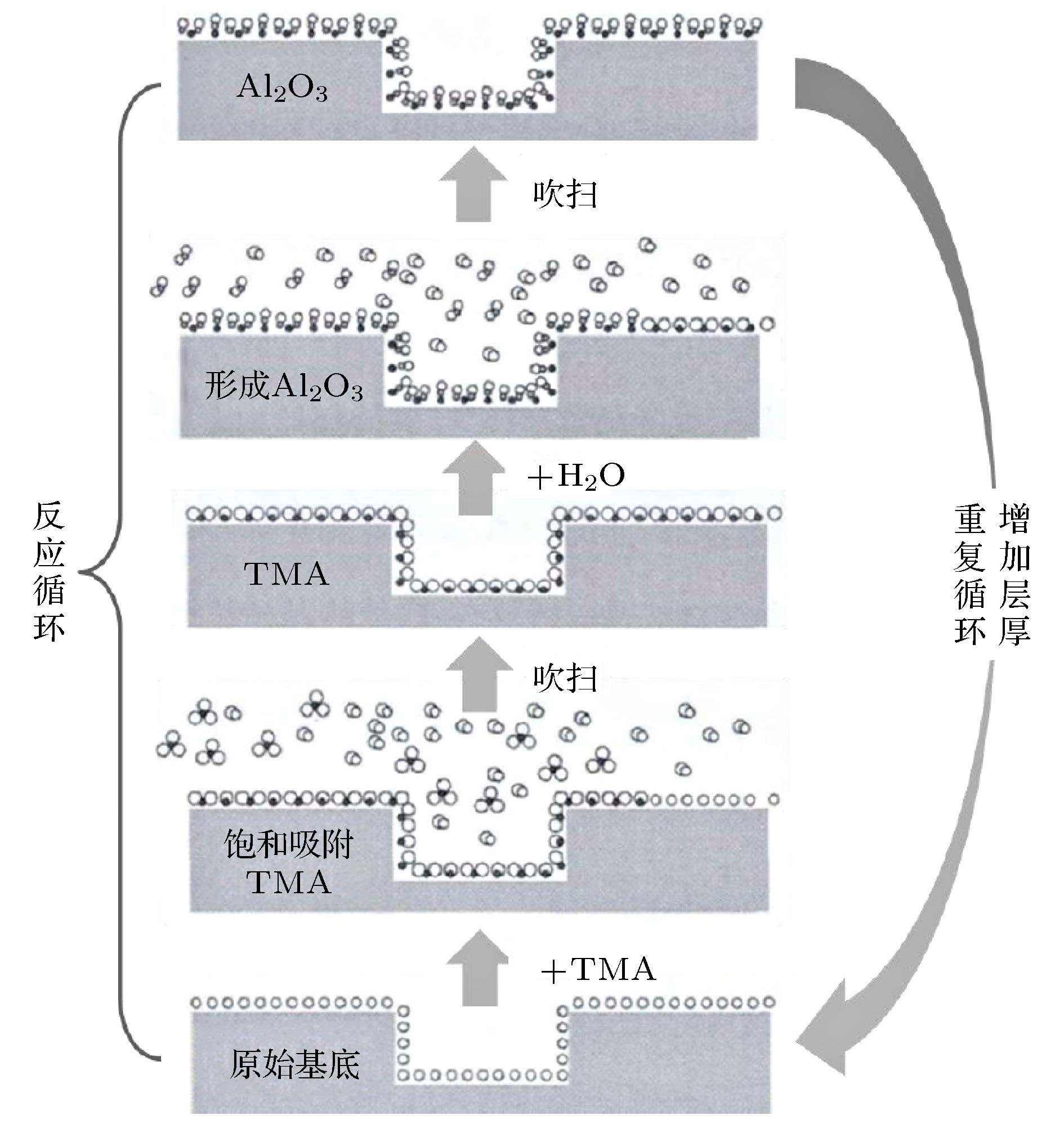
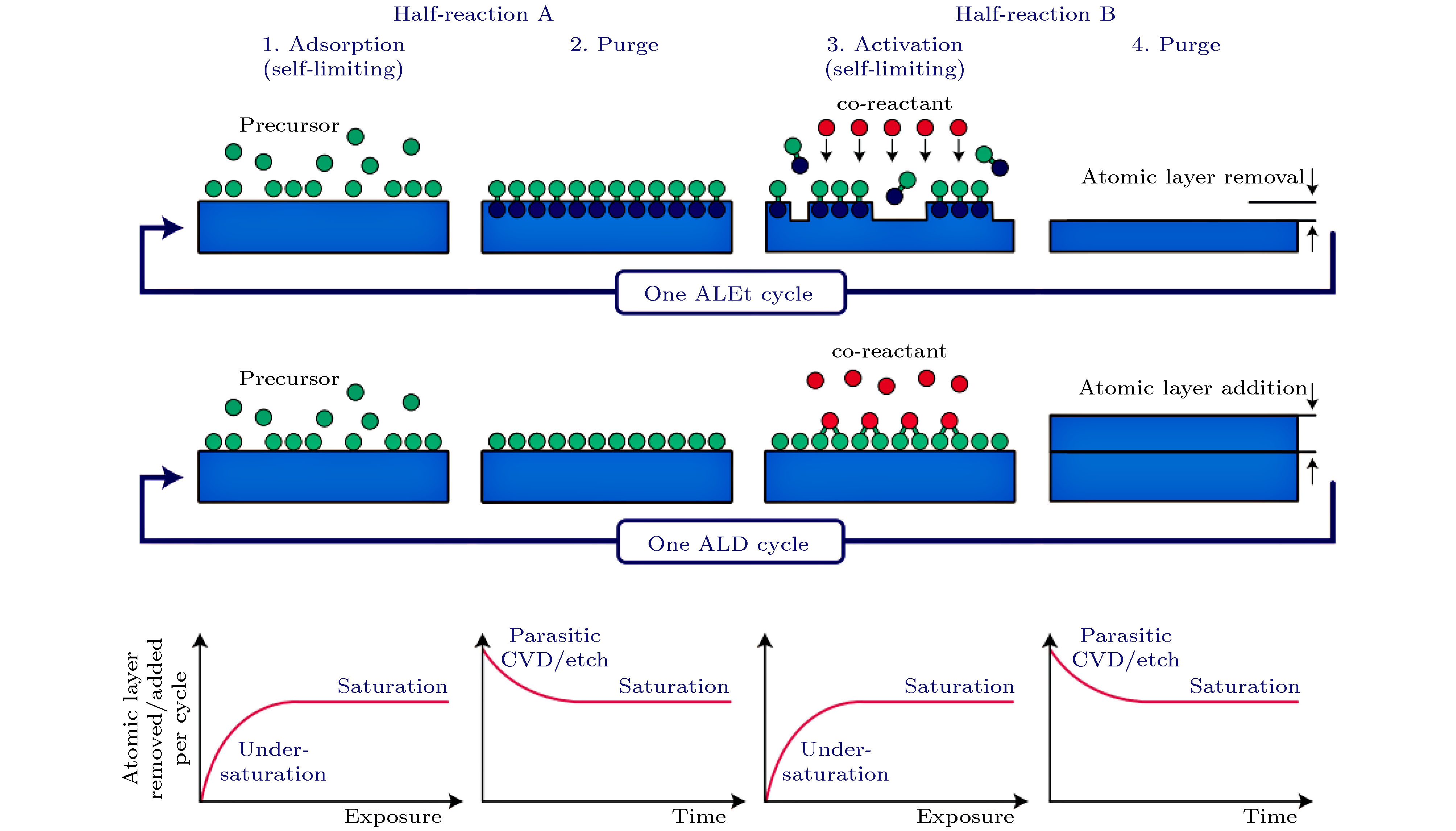
With the development of future information devices towards smaller size, lower power consumption and higher performance, the size of materials used to build devices will be further reduced. Traditional “top-down” technology has encountered a bottleneck in the development of information devices on a nanoscale, while the vapor deposition technology has attracted great attention due to its ability to construct nanostructures on an atomic scale, and is considered to have the most potential to break through the existing manufacturing limits and build nano-structures directly with atoms as a “bottom-up” method. During molecular beam epitaxy, atoms and molecules of materials are deposited on the surface in an “atomic spray painting” way. By such a method, some graphene-like two-dimensional materials (e.g., silicene, germanene, stanene, borophene) have been fabricated with high quality and show many novel electronic properties, and the ultrathin films (several atomic layers) of other materials have been grown to achieve certain purposes, such as NaCl ultrathin layers for decoupling the interaction of metal substrate with the adsorbate. In an atomic layer deposition process, which can be regarded as a special modification of chemical vapor deposition, the film growth takes place in a cyclic manner. The self- limited chemical reactions are employed to insure that only one monolayer of precursor (A) molecules is adsorbed on the surface, and the subsequent self- limited reaction with the other precursor (B) allows only one monolayer of AB materials to be built. And the self- assembled monolayers composed of usually long- chain molecules can be introduced as the active or inactive layer for area- selective atomic layer deposition growth, which is very useful in fabricating nano- patterned structures. As the reverse process of atomic layer deposition, atomic-layer etching processes can remove certain materials in atomic precision. In this paper we briefly introduce the principles of the related technologies and their applications in the field of nano- electronic device processing and manufacturing, and find how to realize the precise control of the thickness and microstructure of functional materials on an atomic scale.
-
Keywords:
- vapor deposition /
- atomic manufacturing /
- molecular beam epitaxy /
- atomic layer deposition
[1] 冯黎, 朱雷 2020 功能材料与器件学报 26 191
Feng L, Zhu L 2020 J. Funct. Mater. Devices 26 191
[2] 庞玉莲, 邹应全 2015 信息记录材料 16 36
 Google Scholar
Pang Y L, Zou Y Q 2015 Info. Rec. Mater. 16 36
Google Scholar
[3] Striccoli M 2017 Science 357 353
Google Scholar
[4] Okazaki S 2015 Microelectron. Eng. 133 23
Google Scholar
[5] Hong F, Blaikie R 2019 Adv. Opt. Mater. 7 1801653
Google Scholar
[6] 王霞, 吕浩, 赵秋玲, 张帅一, 谭永炎 2016 光谱学与光谱分析 36 3461
Wang X, Lü H, Zhao Q L, Zhang S Y, Tan Y Y 2016 Spectrosc. Spect. Anal. 36 3461
[7] Fang F Z 2016 Front. Mech. Eng. Chin. 11 325
Google Scholar
[8] Luo C, Li J F, Yang X, Wu X, Zhong S Y, Wang C L, Sun L T 2020 ACS Appl. Nano Mater. 3 4747
[9] Martín-Palma R J, Lakhtakia A 2013 Engineered Biomimicry (Boston: Elsevier) pp383−398
[10] LaPedus M 2018 工艺与制造 35 39
LaPedus M 2018 Prog. Fabri. 35 39
[11] Ashurbekova K, Ashurbekova K, Botta G, Yurkevich O, Knez M 2020 Nanotechnology 31 342001
Google Scholar
[12] Kulkarni A K 1994 B. Mater. Sci. 17 1379
Google Scholar
[13] Mattox D M 1992 Plat. Surf. Finish. 79 60
[14] Mattox D M 1998 Plat. Surf. Finish. 85 49
[15] Zhu D M, Miller R A, Nagaraj B A, Bruce R W 2001 Surf. Coat. Technol. 138 1
Google Scholar
[16] Muratore C, Walton S G, Leonhardt D, Fernsler R F 2006 J. Vac. Sci. Technol., A 24 25
[17] Kumar T S, Prabu S B, Manivasagam G 2014 J. Mater. Eng. Perform. 23 2877
Google Scholar
[18] Yang R B, Bachmann J, Pippel E, Berger A, Woltersdorf J, Gösele U, Nielsch K 2009 Adv. Mater. 21 3170
Google Scholar
[19] Bao Q H, Chen C Z, Wang D G, Ji Q M, Lei T Q 2005 Appl. Surf. Sci. 252 1538
Google Scholar
[20] Cho A Y, Arthur J R 1975 Prog. Solid State Chem. 10 157
Google Scholar
[21] Hong M 1995 J. Cryst. Growth 150 277
Google Scholar
[22] Spirkoska D, Colombo C, Heiss M, Abstreiter G, Morral A F I 2008 J. Phys. Condens. Matter 20 454225
Google Scholar
[23] Wang X Q, Yoshika A 2011 Thin Film Growth (Sawston Cambridge: Woodhead Publishing) pp288−316
[24] Howson R P, Spencer A G, Lewin R W 1988 Vacuum 38 947
[25] Kelly P J, Arnell R D 2000 Vacuum 56 159
Google Scholar
[26] Shi J Z, Chen C Z, Yu H J, Zhang S J 2008 B. Mater. Sci. 31 877
Google Scholar
[27] Brauer G, Szyszka B, Vergohl M, Bandorf R 2010 Vacuum 84 1354
Google Scholar
[28] Kopecky D, Vrnata M, Kopecka J 2015 Chem. Listy 109 183
[29] von Wenckstern H, Kneiss M, Hassa A, Storm P, Splith D, Grundmann M 2020 Phys. Status Solidi B 257 1900626
Google Scholar
[30] Dabrowska-Szata M 2003 Mater. Chem.Phys. 81 257
Google Scholar
[31] Ichimiya A 2005 J. Jpn. Soc. Tribologis. 50 731
[32] Wood C 1981 Surf. Sci. 108 L441
[33] Chang C Z, Zhang J S, Feng X, Shen J, Zhang Z C, Guo M H, Li K, Ou Y B, Wei P, Wang L L, Ji Z Q, Feng Y, Ji S H, Chen X, Jia J F, Dai X, Fang Z, Zhang S C, He K, Wang Y Y, Lu L, Ma X C, Xue Q K 2013 Science 340 167
Google Scholar
[34] Zhang J S, Chang C Z, Tang P Z, Zhang Z C, Feng X, Li K, Wang L L, Chen X, Liu C X, Duan W H, He K, Xue Q K, Ma X C, Wang Y Y 2013 Science 339 1582
Google Scholar
[35] Fei F, Zhang S, Zhang M, Shah S A, Song F, Wang X, Wang B 2019 Adv. Mater. 32 1904593
[36] Guo Q M, Qin Z H, Liu C D, Zang K, Yu Y H, Cao G Y 2010 Surf. Sci. 604 1820
Google Scholar
[37] Li L F, Lu S Z, Pan J B, Qin Z H, Wang Y Q, Wang Y L, Cao G Y, Du S X, Gao H J 2014 Adv. Mater. 26 4820
Google Scholar
[38] Qin Z H, Pan J B, Lu S Z, Yan S, Wang Y L, Du S X, Gao H J, Cao G Y 2017 Adv. Mater. 29 1606046
Google Scholar
[39] Liao M H, Zang Y Y, Guan Z Y, Li H W, Gong Y, Zhu K J, Hu X P, Zhang D, Xu Y, Wang Y Y, He K, Ma X C, Zhang S C, Xue Q K 2018 Nat. Phys. 14 344
Google Scholar
[40] 秦志辉 2017 物理学报 66 216802
Google Scholar
Qin Z H 2017 Acta Phys. Sin. 66 216802
Google Scholar
[41] Qin Z 2013 Chin. Phys. B 22 098108
Google Scholar
[42] Cahangirov S, Topsakal M, Aktürk E, Şahin H, Ciraci S 2009 Phys. Rev. Lett. 102 236804
Google Scholar
[43] Liu C C, Feng W X, Yao Y G 2011 Phys. Rev. Lett. 107 076802
Google Scholar
[44] Le Lay G 2015 Nat. Nanotechnol. 10 202
Google Scholar
[45] Dávila M E, Xian L, Cahangirov S, Rubio A, Le Lay G 2014 New J. Phys. 16 095002
Google Scholar
[46] Derivaz M, Dentel D, Stephan R, Hanf M C, Mehdaoui A, Sonnet P, Pirri C 2015 Nano Lett. 15 2510
Google Scholar
[47] Meng L, Wang Y L, Zhang L Z, Du S X, Wu R T, Li L F, Zhang Y, Li G, Zhou H T, Hofer W A, Gao H J 2013 Nano Lett. 13 685
Google Scholar
[48] Feng B J, Zhang J, Zhong Q, Li W B, Li S, Li H, Cheng P, Meng S, Chen L, Wu K H 2016 Nat. Chem. 8 564
[49] Feng B, Zhang J, Zhong Q, Li W, Li S, Li H, Cheng P, Meng S, Chen L, Wu K 2016 Nat. Chem. 8 563
Google Scholar
[50] Penev E S, Kutana A, Yakobson B I 2016 Nano Lett. 16 2522
Google Scholar
[51] Li L F, Wang Y L, Xie S Y, Li X B, Wang Y Q, Wu R T, Sun H B, Zhang S B, Gao H J 2013 Nano Lett. 13 4671
Google Scholar
[52] Guo Q, Zhong Y, Huang M, Lu S, Yu Y 2020 Thin Solid Films 693 137709
Google Scholar
[53] Guo Q M, Qin Z H, Huang M, Mantsevich V N, Cao G Y 2016 Chin. Phys. B 25 036801
Google Scholar
[54] Beinik I, Barth C, Hanbucken M, Masson L 2015 Sci. Rep. 5 8223
Google Scholar
[55] Kwong P, Seidel S, Gupta M 2015 J. Vac. Sci. Technol., A 33 031504
Google Scholar
[56] McGinn P J 2019 ACS Comb. Sci. 21 501
Google Scholar
[57] Nie Z, Shi Y, Qin S, Wang Y, Jiang H, Zheng Q, Cui Y, Meng Y, Song F, Wang X, Turcu I C E, Wang X, Xu Y, Shi Y, Zhao J, Zhang R, Wang F 2019 Commun. Phys. 2 103
Google Scholar
[58] Triboulet R 2014 Prog. Cryst. Growth Charact. Matter. 60 1
Google Scholar
[59] Wang X R, Yushin G 2015 Energy Environ. Sci. 8 1889
Google Scholar
[60] Yu S J, Pak K, Kwak M J, Joo M, Kim B J, Oh M S, Baek J, Park H, Choi G, Kim D H, Choi J, Choi Y, Shin J, Moon H, Lee E, Im S G 2018 Adv. Eng. Mater. 20 1700622
Google Scholar
[61] Keyshar K, Gong Y J, Ye G L, Brunetto G, Zhou W, Cole D P, Hackenberg K, He Y M, Machado L, Kabbani M, Hart A H C, Li B, Galvao D S, George A, Vajtai R, Tiwary C S, Ajayan P M 2015 Adv. Mater. 27 4640
Google Scholar
[62] Matsuda T, Sato J, Ishikawa T, Ogino A, Nagatsu M 2009 Diam. Relat. Mater. 18 548
Google Scholar
[63] Shukla B, Saito T, Yumura M, Iijima S 2009 Chem. Commun. 342 2
[64] Chen H C, Su W R, Yeh Y C 2020 ACS Appl. Mater. Interfaces 12 32905
Google Scholar
[65] Novoselov K S, Geim A K, Morozov S V, Jiang D, Zhang Y, Dubonos S V, Grigorieva I V, Firsov A A 2004 Science 306 666
Google Scholar
[66] Kim M, Safron N S, Han E, Arnold M S, Gopalan P 2010 Nano Lett. 10 1125
Google Scholar
[67] Kim Y, Choi D S, Kim H J, Kim H, Kim T Y, Rhyu S H, Lee K S, Yoon D H, Yang W S 2014 J. Ceram. Process. Res. 15 269
[68] Fang W J, Hsu A L, Song Y, Kong J 2015 Nanoscale 7 20335
Google Scholar
[69] Sun H, Xu J, Wang C, Ge G, Jia Y, Liu J, Song F, Wan J 2016 Carbon 108 356
Google Scholar
[70] Sun H, Fu C, Shen X, Yang W, Guo P, Lu Y, Luo Y, Yu B, Wang X, Wang C, Xu J, Liu J, Song F, Wang G, Wan J 2017 Nanotechnology 28 245604
Google Scholar
[71] Tan H, Wang D G, Guo Y B 2018 Coatings 8 40
Google Scholar
[72] Jessen B S, Gammelgaard L, Thomsen M R, Mackenzie D M A, Thomsen J D, Caridad J M, Duegaard E, Watanabe K, Taniguchi T, Booth T J, Pedersen T G, Jauho A P, Boggild P 2019 Nat. Nanotechnol. 14 340
Google Scholar
[73] Wu J, Li Y, Pan D, Jiang C, Jin C, Song F, Wang G, Wan J 2019 Carbon 147 434
Google Scholar
[74] Jia K, Ci H, Zhang J, Sun Z, Ma Z, Zhu Y, Liu S, Liu J, Sun L, Liu X, Sun J, Yin W, Peng H, Lin L, Liu Z 2020 Angew. Chem. Int. Ed. 59 17214
Google Scholar
[75] Li X, Cai W, Colombo L, Ruoff R S 2009 Nano Lett. 9 4268
Google Scholar
[76] Puurunen R L 2005 J. Appl. Phys. 97 121301
Google Scholar
[77] Kol'tsov S I, Aleskovskii V B 1967 Zh. Prikl. Khim. 40 907
[78] Kol'tsov S I, Aleskovskii V B 1969 Zh. Prikl. Khim. 42 1023
[79] Suntola T, Antson J U.S. Patent 4058430 [1977-11-15]
[80] Longo E, Mantovan R, Cecchini R, Overbeek M D, Longo M, Trevisi G, Lazzarini L, Tallarida G, Fanciulli M, Winter C H, Wiemer C 2020 Nano Res. 13 570
Google Scholar
[81] Ahvenniemi E, Karppinen M 2016 Dalton Trans. 45 10730
Google Scholar
[82] Leskelä M, Ritala M 2003 Angew. Chem. Int. Ed. 42 5548
Google Scholar
[83] Yang H C, Waldman R Z, Chen Z W, Darling S B 2018 Nanoscale 10 20505
Google Scholar
[84] Griffiths M B E, Pallister P J, Mandia D J, Barry S T 2016 Chem. Mater. 28 44
Google Scholar
[85] Ahn J, Ahn C, Jeon S, Park J 2019 Appl. Sci. 9 1990
Google Scholar
[86] Marichy C, Bechelany M, Pinna N 2012 Adv. Mater. 24 1017
Google Scholar
[87] Ovanesyan R A, Filatova E A, Elliott S D, Hausmann D M, Smith D C, Agarwal S 2019 J. Vac. Sci. Technol., A 37 060904
Google Scholar
[88] Solanki R, Huo J, Freeouf J L, Miner B 2002 Appl. Phys. Lett. 81 3864
Google Scholar
[89] Andou Y, Nishida H, Endo T 2006 Chem. Commun. 501 8
[90] Amitonova L V, de Boer J F 2020 Light-Sci. Appl. 9 81
Google Scholar
[91] Clary J, Norman S, Funke H, Su D, Musgrave C, Weimer A 2020 Nanotechnology 31 175703
Google Scholar
[92] Cao K, Cai J, Chen R 2020 Chem. Mater. 32 2195
Google Scholar
[93] Shimamura H, Nakamura T 2010 Polym. Degrad. Stab. 95 21
Google Scholar
[94] Klesko J P, Kerrigan M M, Winter C H 2016 Chem. Mater. 28 700
Google Scholar
[95] Kerrigan M M, Klesko J P, Winter C H 2017 Chem. Mater. 29 7458
Google Scholar
[96] Knisley T J, Kalutarage L C, Winter C H 2013 Coord. Chem. Rev. 257 3222
Google Scholar
[97] Eigenfeld N T, Gray J M, Brown J J, Skidmore G D, George S M, Bright V M 2014 Adv. Mater. 26 3962
Google Scholar
[98] Knisley T J, Saly M J, Heeg M J, Roberts J L, Winter C H 2011 Organometallics 30 5010
Google Scholar
[99] Krozer A, Rodahl M 1997 J. Vac. Sci. Technol., A 15 1704
Google Scholar
[100] Chen R, Bent S F 2006 Adv. Mater. 18 1086
Google Scholar
[101] Wojtecki R, Mettry M, Fine Nathel N F, Friz A, De Silva A, Arellano N, Shobha H 2018 ACS Appl. Mater. Interfaces 10 38630
Google Scholar
[102] Koenig M, Lahann J 2017 Beilstein J. Nanotechnol. 8 1250
Google Scholar
[103] Chang Y H, Liu C M, Tseng Y C, Chen C, Chen C C, Cheng H E 2010 Nanotechnology 21 225602
Google Scholar
[104] Kim S W, Han T H, Kim J, Gwon H, Moon H S, Kang S W, Kim S O, Kang K 2009 ACS Nano 3 1085
Google Scholar
[105] Ban C M, George S M 2016 Adv. Mater. Interfaces 3 1600762
Google Scholar
[106] Liu L, Karuturi S K, Su L T, Tok A I Y 2011 Energy Environ. Sci. 4 209
Google Scholar
[107] Mackus A J M, Bol A A, Kessels W M M 2014 Nanoscale 6 10941
Google Scholar
[108] Skoog S A, Elam J W, Narayan R J 2013 Int. Mater. Rev. 58 113
Google Scholar
[109] Szilagyi I M, Teucher G, Harkonen E, Farm E, Hatanpaa T, Nikitin T, Khriachtchev L, Rasanen M, Ritala M, Leskela M 2013 Nanotechnology 24 245701
Google Scholar
[110] Gebhard M, Mitschker F, Hoppe C, Aghaee M, Rogalla D, Creatore M, Grundmeier G, Awakowicz P, Devi A 2018 Plasma Process. Polym. 15 e1700209
Google Scholar
[111] Kim K M, Jang J S, Yoon S G, Yun J Y, Chung N K 2020 Materials 13 2008
Google Scholar
[112] Choudhury D, Sarkar S K 2014 Chem. Vapor Depos. 20 130
Google Scholar
[113] Yoshimura T 2016 Macromol. Symp. 361 141
Google Scholar
[114] Poodt P, Cameron D C, Dickey E, George S M, Kuznetsov V, Parsons G N, Roozeboom F, Sundaram G, Vermeer A 2012 J. Vac. Sci. Technol., A 30 010802
Google Scholar
[115] Poodt P, van Lieshout J, Illiberi A, Knaapen R, Roozeboom F, van Asten A 2013 J. Vac. Sci. Technol., A 31 01A108
[116] Sharma K, Hall R A, George S M 2015 J. Vac. Sci. Technol., A 33 01A132
Google Scholar
[117] Mousa M B M, Ovental J S, Brozena A H, Oldham C J, Parsons G N 2018 J. Vac. Sci. Technol., A 36 031517
Google Scholar
[118] Satpati A K, Arroyo-Curras N, Ji L, Yu E T, Bard A J 2013 Chem. Mater. 25 4165
Google Scholar
[119] Venkatraman K, Gusley R, Lesak A, Akolkar R 2019 J. Vac. Sci. Technol., A 37 020901
Google Scholar
[120] Elam J W 2012 Atomic Layer Deposition of Nanostructured Materials (Weinheim: Wiley-VCH Verlag GmbH & Co. KGaA) pp227−249
[121] Chen R, Kim H, McIntyre P C, Porter D W, Bent S F 2005 Appl. Phys. Lett. 86 191910
Google Scholar
[122] Lee H B R, Bent S F 2012 Atomic Layer Deposition of Nanostructured Materials (Weinheim: Wiley-VCH Verlag GmbH & Co. KGaA) pp193−225
[123] Hashemi F S M, Prasittichai C, Bent S F 2014 J. Phys. Chem. C 118 10957
Google Scholar
[124] Minaye Hashemi F S, Prasittichai C, Bent S F 2015 ACS Nano 9 8710
Google Scholar
[125] Hashemi F S M, Bent S F 2016 Adv. Mater. Interfaces 3 1600464
Google Scholar
[126] Seo S, Yeo B C, Han S S, Yoon C M, Yang J Y, Yoon J, Yoo C, Kim H J, Lee Y B, Lee S J, Myoung J M, Lee H B R, Kim W H, Oh I K, Kim H 2017 ACS Appl. Mater. Interfaces 9 41607
Google Scholar
[127] Farm E, Kemell M, Santala E, Ritala M, Leskela M 2010 J. Electrochem. Soc. 157 K10
Google Scholar
[128] Lee W, Prinz F B 2009 J. Electrochem. Soc. 156 G125
Google Scholar
[129] Horiike Y, Tanaka T, Nakano M, Iseda S, Sakaue H, Nagata A, Shindo H, Miyazaki S, Hirose M 1990 J. Vac. Sci. Technol., A 8 1844
Google Scholar
[130] Athavale S D 1996 J. Vac. Sci. Technol., B 14 3702
Google Scholar
[131] Dimiev A, Kosynkin D V, Sinitskii A, Slesarev A, Sun Z, Tour J M 2011 Science 331 1168
Google Scholar
[132] Faraz T, Roozeboom F, Knoops H, Kessels W M M 2015 ECS J. Solid State SC 4 N5023
[133] Lee Y, DuMont J W, George S M 2015 Chem. Mater. 27 3648
Google Scholar
[134] Oehrlein G, Metzler D, Li C 2015 ECS J. Solid State SC 4 N5041
[135] Kauppinen C, Khan S A, Sundqvist J, Suyatin D B, Suihkonen S, Kauppinen E I, Sopanen M 2017 J. Vac. Sci. Technol., A 35 060603
Google Scholar
[136] Kim K S, Ji Y J, Nam Y, Kim K H, Singh E, Lee J Y, Yeom G Y 2017 Sci. Rep. 7 2462
Google Scholar
[137] Kim K S, Kim K H, Nam Y, Jeon J, Yim S, Singh E, Lee J Y, Lee S J, Jung Y S, Yeom G Y, Kim D W 2017 ACS Appl. Mater. Interfaces 9 11967
Google Scholar
[138] Park J W, Kim D S, Mun M K, Lee W O, Kim K S, Yeom G Y 2017 J. Phys. D: Appl. Phys. 50 254007
Google Scholar
[139] Shinoda K, Miyoshi N, Kobayashi H, Kurihara M, Izawa M, Ishikawa K, Hori M 2017 ECS Trans. 80 3
[140] Abdulagatov A I, George S M 2018 Chem. Mater. 30 8465
Google Scholar
[141] Cheng Y, Wang K, Qi Y, Liu Z 2020 Acta Phys.-Chim. Sin. 2021 37
[142] Wang M, Fu L, Gan L, Zhang C, Rummeli M, Bachmatiuk A, Huang K, Fang Y, Liu Z 2013 Sci. Rep. 3 1238
Google Scholar
-

图 1 MBE系统结构示意图
Figure 1. Schematic diagram of MBE system.
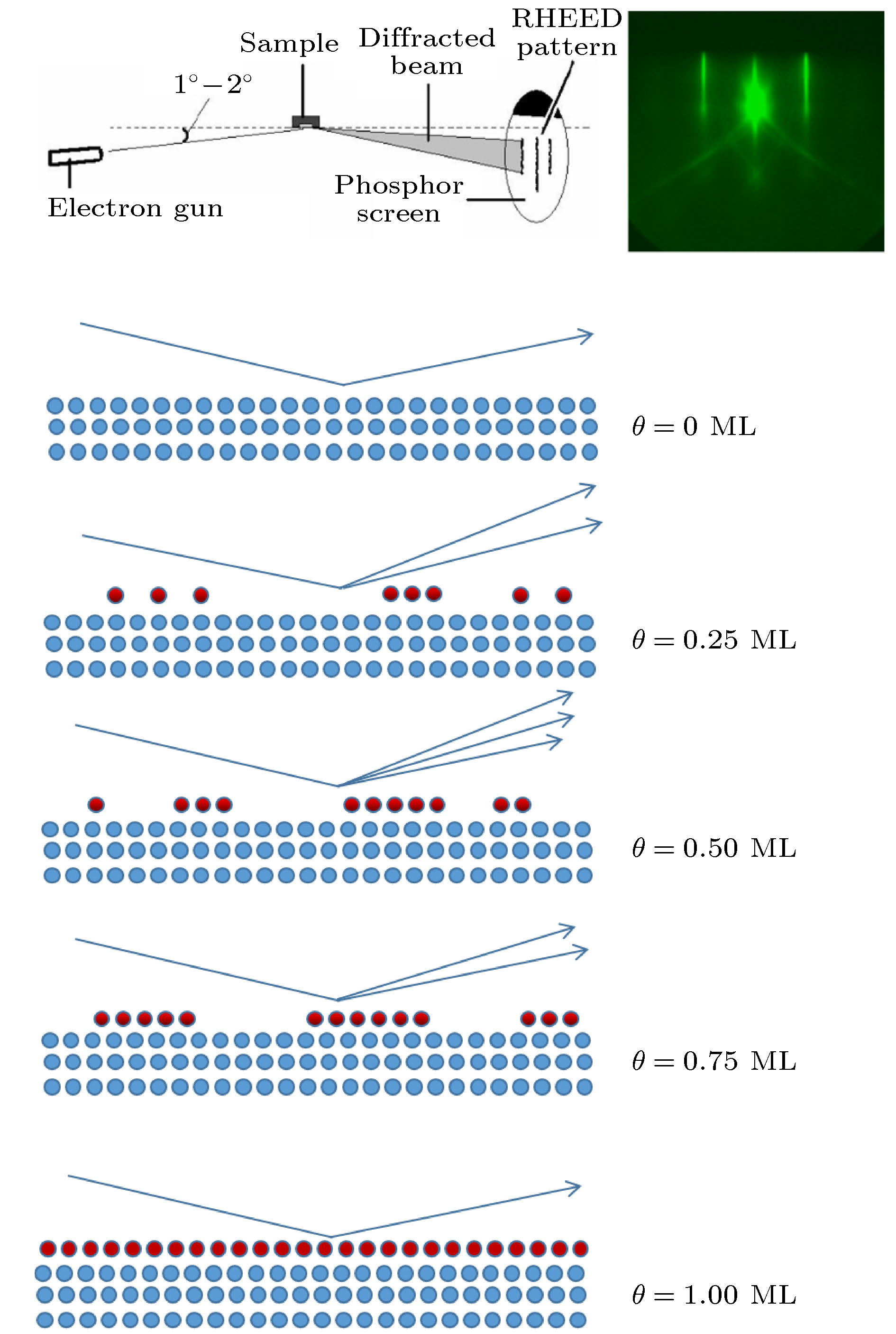
图 2 RHEED系统示意图和漫反射现象随着薄膜生长的关系示意图
Figure 2. Schematic diagram of RHEED, and the relationship between diffuse reflection and film coverage during growth.
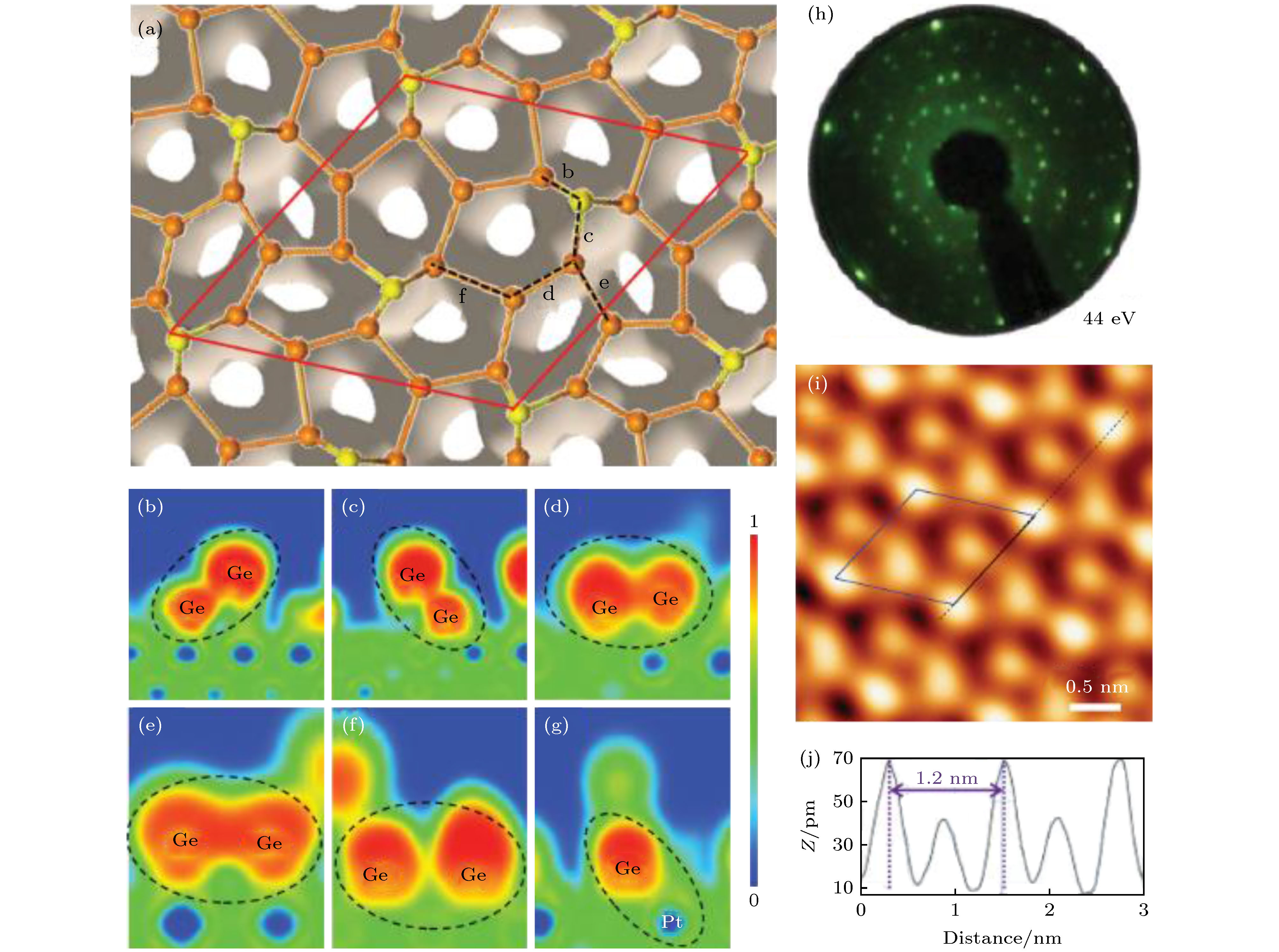
图 3 (a) Pt(111)表面锗烯的理论计算结构; (b)−(g) 不同位置的Ge原子对以及Ge单原子与最近邻基底Pt原子间电子局域函数的计算模拟; (h)−(j) 锗烯的实验结果(LEED, STM图像及表观高度)[37]
Figure 3. (a) Theoretical model of germanene on Pt (111) surface, and the electron localization functions of the cross-sections between the germanium pairs (b)−(f) and between one germanium atom and its nearest Pt neighbor (g). (h)−(j) The experimental results of LEED pattern, STM image and the apparent height along the indicated line in the STM image, respectively[37].

图 4 (a) Cu(111)表面制备的锗烯; (b), (c) Cu(111)基底和锗烯的原子分辨图像; (d) 双层锗烯的吸附结构模型; (e) 相应的STM图像模拟, 与实验结果(c)吻合; (f) 单层(红色)和双层(黑色)锗烯的电子结构(STS谱), 插图为Cu(111)基底STS谱用于标定针尖状态[38]
Figure 4. (a) STM image of germanene on Cu(111); (b), (c) the atomic-resolved STM images of Cu (111) substrate and germanene, respectively; (d) the adsorption model of bilayer germanene; (e) the simulated STM image with the features fitting very well with the experimental observations; (f) the STS of monolayer (red) and bilayer (black) germanene, and inset is STS taken on the bare Cu(111) to verify the condition of the tip[38].
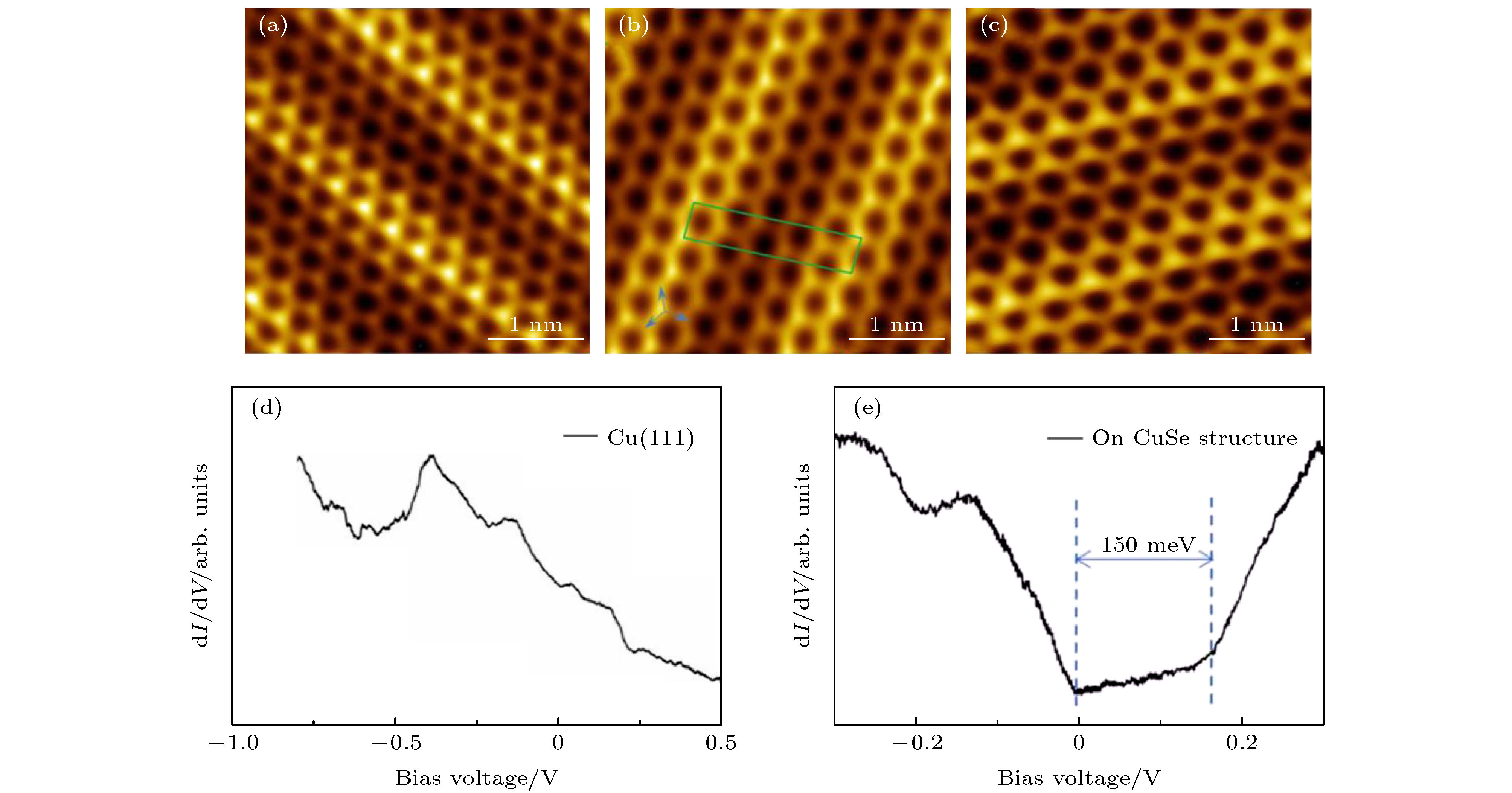
图 5 (a)−(c) 在Cu(111)表面MBE生长的不同取向的硒化铜蜂窝状结构的STM图像; (d) 用于标定针尖状态的Cu(111)表面标准STS谱; (e) CuSe结构的STS谱[52]
Figure 5. (a)−(c) The STM images of honeycomb structures with equivalent orientations on Cu(111) by means of MBE growth; (d) the standard STS of Cu(111) for checking tip status; (e) electronic structure (STS) of CuSe structures[52].
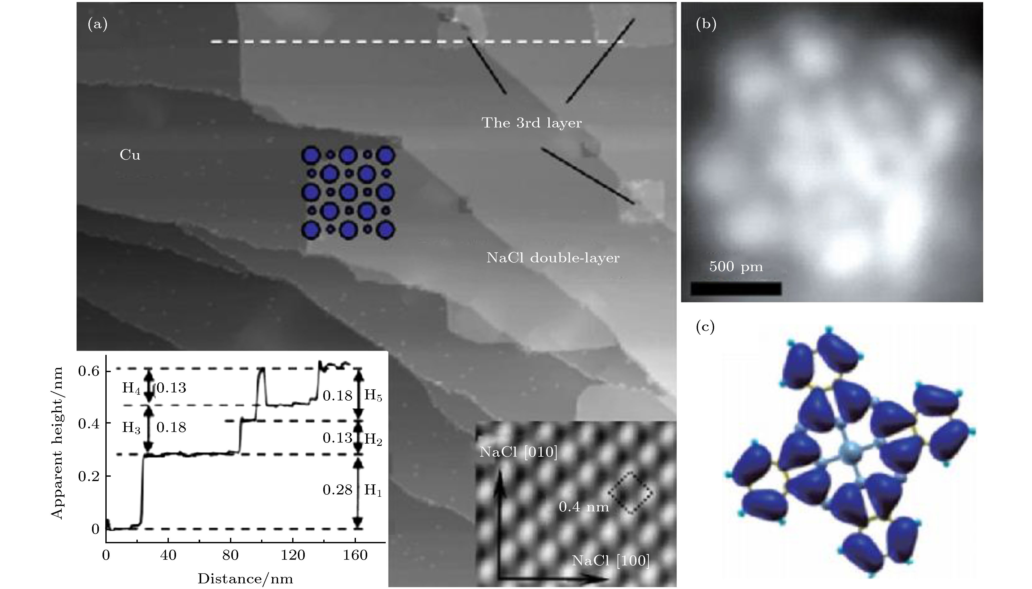
图 6 (a) 在Cu(100)上外延生长的NaCl薄膜[36], 以及在其上的CoPc分子轨道的实验(b)和理论(c)图像[53]
Figure 6. (a) MBE growth of NaCl layers on Cu(100)[36], on top of which the quasi-free molecular orbital of adsorbed CoPc can be observed. (b) and (c) are the STM image and theoretical simulation of molecular orbital, respectively[53].
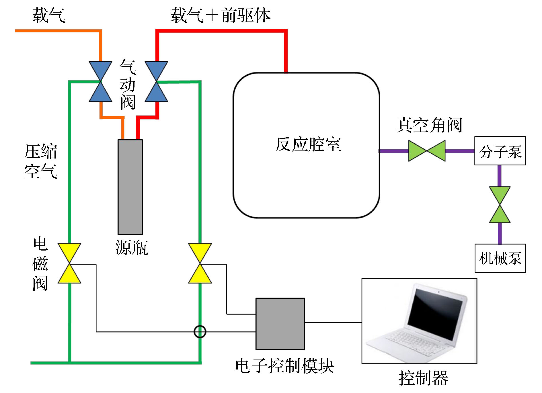
图 8 原子层沉积系统示意图
Figure 8. Schematic diagram of atomic layer deposition system.
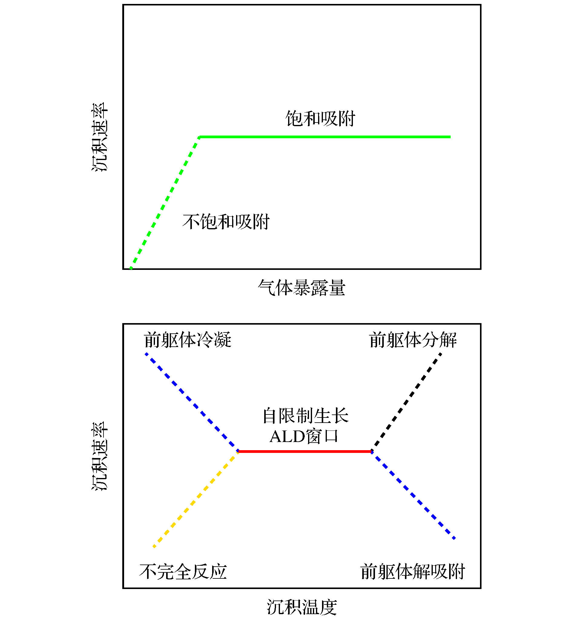
图 11 气体前驱体暴露量和沉积温度对原子层沉积镀膜速率的影响
Figure 11. Effects of gaseous precursor exposure and deposition temperature on deposition rate of atomic layers.
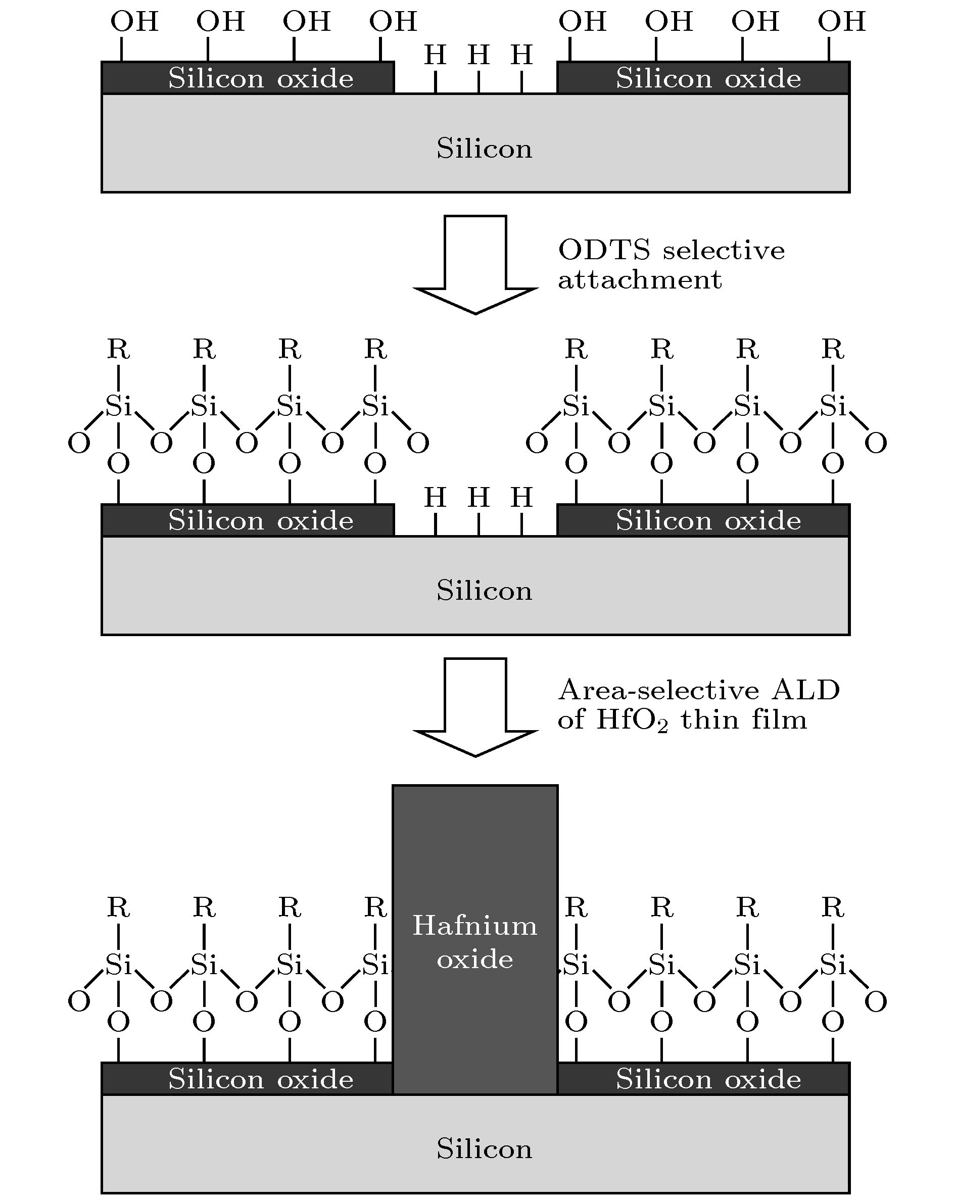
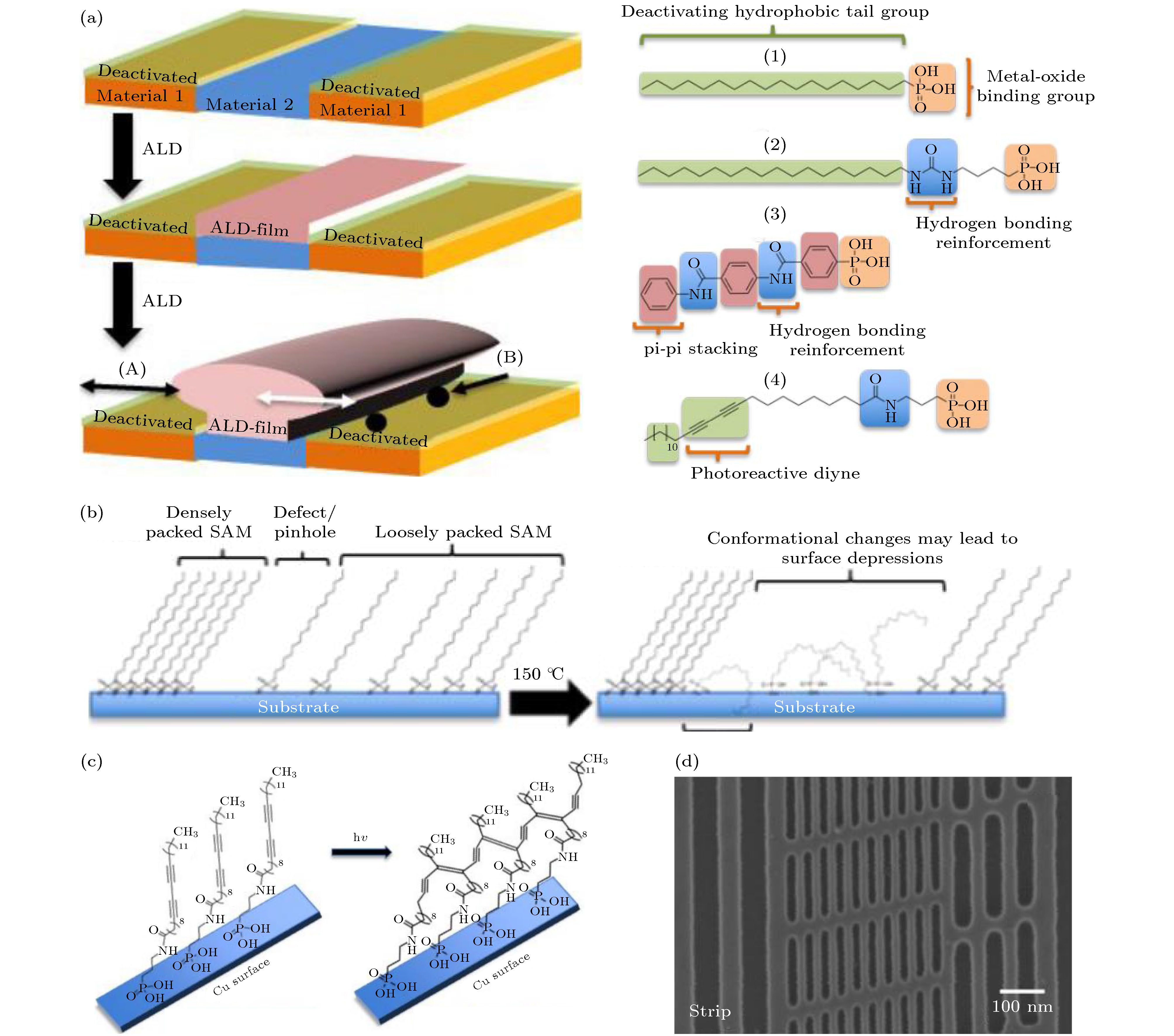
图 13 (a) 左边选区ALD的原理示意图, 右边为自组装钝化层的单体分子结构; (b) 自组装薄膜的缺陷(pinhole)影响ALD沉积过程的选择性; (c) 自组装分子的光聚合官能团(二炔基)在光诱导下聚合有效抑制缺陷产生; (d) 通过选区ALD沉积ZnO掩膜刻蚀后的微结构, 结构最窄宽度约为15 nm[101]
Figure 13. (a) Schematic diagram of area-selective ALD growth (left), and the monomer molecular structures forming inactive SAMs (right); (b) the pinhole defect affects the selectivity of ALD deposition; (c) photopolymeric functional groups (diacetylenyl) of SAMs can effectively inhibit defect formation in terms of photo-induced polymerization; (d) SEM micrograph of the microstructure obtained by etching with ZnO mask of area-selective ALD, and the width of narrowest structure reaches 15 nm[101].
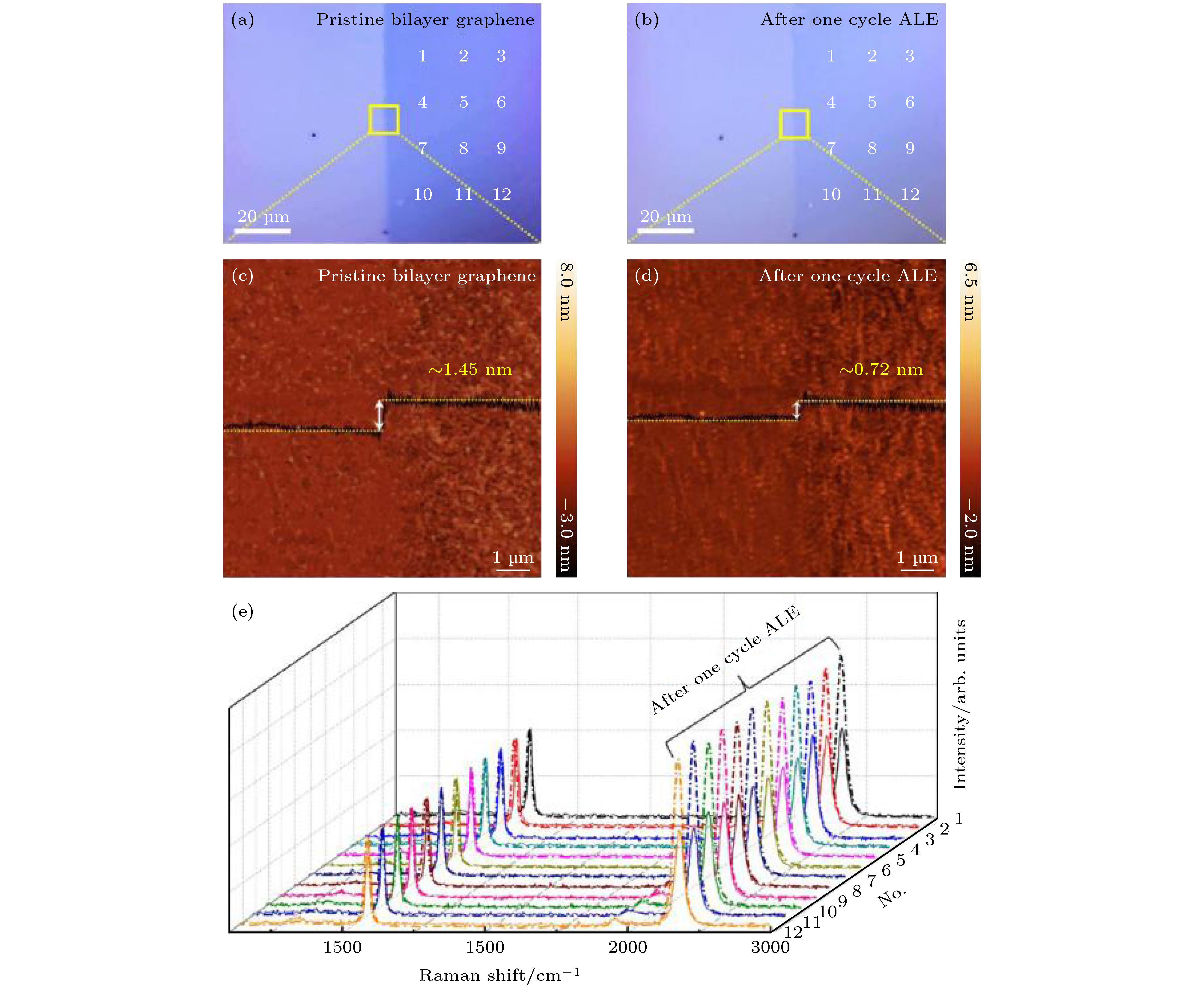
图 15 双层石墨烯ALE刻蚀前后的光学显微图像(a), (b)以及相应的AFM图像(c), (d)和在各位点的拉曼谱(e)[136]
Figure 15. Optical microscopic images (a), (b) and AFM images (c), (d) of bilayer graphene before and after one cycle of ALE etching. (e) Raman spectrum of graphene taken at twelve points indicated in (a), (b) before and after etching[136].

-
[1] 冯黎, 朱雷 2020 功能材料与器件学报 26 191
Feng L, Zhu L 2020 J. Funct. Mater. Devices 26 191
[2] 庞玉莲, 邹应全 2015 信息记录材料 16 36
Google Scholar
Pang Y L, Zou Y Q 2015 Info. Rec. Mater. 16 36
Google Scholar
[3] Striccoli M 2017 Science 357 353
Google Scholar
[4] Okazaki S 2015 Microelectron. Eng. 133 23
Google Scholar
[5] Hong F, Blaikie R 2019 Adv. Opt. Mater. 7 1801653
Google Scholar
[6] 王霞, 吕浩, 赵秋玲, 张帅一, 谭永炎 2016 光谱学与光谱分析 36 3461
Wang X, Lü H, Zhao Q L, Zhang S Y, Tan Y Y 2016 Spectrosc. Spect. Anal. 36 3461
[7] Fang F Z 2016 Front. Mech. Eng. Chin. 11 325
Google Scholar
[8] Luo C, Li J F, Yang X, Wu X, Zhong S Y, Wang C L, Sun L T 2020 ACS Appl. Nano Mater. 3 4747
[9] Martín-Palma R J, Lakhtakia A 2013 Engineered Biomimicry (Boston: Elsevier) pp383−398
[10] LaPedus M 2018 工艺与制造 35 39
LaPedus M 2018 Prog. Fabri. 35 39
[11] Ashurbekova K, Ashurbekova K, Botta G, Yurkevich O, Knez M 2020 Nanotechnology 31 342001
Google Scholar
[12] Kulkarni A K 1994 B. Mater. Sci. 17 1379
Google Scholar
[13] Mattox D M 1992 Plat. Surf. Finish. 79 60
[14] Mattox D M 1998 Plat. Surf. Finish. 85 49
[15] Zhu D M, Miller R A, Nagaraj B A, Bruce R W 2001 Surf. Coat. Technol. 138 1
Google Scholar
[16] Muratore C, Walton S G, Leonhardt D, Fernsler R F 2006 J. Vac. Sci. Technol., A 24 25
[17] Kumar T S, Prabu S B, Manivasagam G 2014 J. Mater. Eng. Perform. 23 2877
Google Scholar
[18] Yang R B, Bachmann J, Pippel E, Berger A, Woltersdorf J, Gösele U, Nielsch K 2009 Adv. Mater. 21 3170
Google Scholar
[19] Bao Q H, Chen C Z, Wang D G, Ji Q M, Lei T Q 2005 Appl. Surf. Sci. 252 1538
Google Scholar
[20] Cho A Y, Arthur J R 1975 Prog. Solid State Chem. 10 157
Google Scholar
[21] Hong M 1995 J. Cryst. Growth 150 277
Google Scholar
[22] Spirkoska D, Colombo C, Heiss M, Abstreiter G, Morral A F I 2008 J. Phys. Condens. Matter 20 454225
Google Scholar
[23] Wang X Q, Yoshika A 2011 Thin Film Growth (Sawston Cambridge: Woodhead Publishing) pp288−316
[24] Howson R P, Spencer A G, Lewin R W 1988 Vacuum 38 947
[25] Kelly P J, Arnell R D 2000 Vacuum 56 159
Google Scholar
[26] Shi J Z, Chen C Z, Yu H J, Zhang S J 2008 B. Mater. Sci. 31 877
Google Scholar
[27] Brauer G, Szyszka B, Vergohl M, Bandorf R 2010 Vacuum 84 1354
Google Scholar
[28] Kopecky D, Vrnata M, Kopecka J 2015 Chem. Listy 109 183
[29] von Wenckstern H, Kneiss M, Hassa A, Storm P, Splith D, Grundmann M 2020 Phys. Status Solidi B 257 1900626
Google Scholar
[30] Dabrowska-Szata M 2003 Mater. Chem.Phys. 81 257
Google Scholar
[31] Ichimiya A 2005 J. Jpn. Soc. Tribologis. 50 731
[32] Wood C 1981 Surf. Sci. 108 L441
[33] Chang C Z, Zhang J S, Feng X, Shen J, Zhang Z C, Guo M H, Li K, Ou Y B, Wei P, Wang L L, Ji Z Q, Feng Y, Ji S H, Chen X, Jia J F, Dai X, Fang Z, Zhang S C, He K, Wang Y Y, Lu L, Ma X C, Xue Q K 2013 Science 340 167
Google Scholar
[34] Zhang J S, Chang C Z, Tang P Z, Zhang Z C, Feng X, Li K, Wang L L, Chen X, Liu C X, Duan W H, He K, Xue Q K, Ma X C, Wang Y Y 2013 Science 339 1582
Google Scholar
[35] Fei F, Zhang S, Zhang M, Shah S A, Song F, Wang X, Wang B 2019 Adv. Mater. 32 1904593
[36] Guo Q M, Qin Z H, Liu C D, Zang K, Yu Y H, Cao G Y 2010 Surf. Sci. 604 1820
Google Scholar
[37] Li L F, Lu S Z, Pan J B, Qin Z H, Wang Y Q, Wang Y L, Cao G Y, Du S X, Gao H J 2014 Adv. Mater. 26 4820
Google Scholar
[38] Qin Z H, Pan J B, Lu S Z, Yan S, Wang Y L, Du S X, Gao H J, Cao G Y 2017 Adv. Mater. 29 1606046
Google Scholar
[39] Liao M H, Zang Y Y, Guan Z Y, Li H W, Gong Y, Zhu K J, Hu X P, Zhang D, Xu Y, Wang Y Y, He K, Ma X C, Zhang S C, Xue Q K 2018 Nat. Phys. 14 344
Google Scholar
[40] 秦志辉 2017 物理学报 66 216802
Google Scholar
Qin Z H 2017 Acta Phys. Sin. 66 216802
Google Scholar
[41] Qin Z 2013 Chin. Phys. B 22 098108
Google Scholar
[42] Cahangirov S, Topsakal M, Aktürk E, Şahin H, Ciraci S 2009 Phys. Rev. Lett. 102 236804
Google Scholar
[43] Liu C C, Feng W X, Yao Y G 2011 Phys. Rev. Lett. 107 076802
Google Scholar
[44] Le Lay G 2015 Nat. Nanotechnol. 10 202
Google Scholar
[45] Dávila M E, Xian L, Cahangirov S, Rubio A, Le Lay G 2014 New J. Phys. 16 095002
Google Scholar
[46] Derivaz M, Dentel D, Stephan R, Hanf M C, Mehdaoui A, Sonnet P, Pirri C 2015 Nano Lett. 15 2510
Google Scholar
[47] Meng L, Wang Y L, Zhang L Z, Du S X, Wu R T, Li L F, Zhang Y, Li G, Zhou H T, Hofer W A, Gao H J 2013 Nano Lett. 13 685
Google Scholar
[48] Feng B J, Zhang J, Zhong Q, Li W B, Li S, Li H, Cheng P, Meng S, Chen L, Wu K H 2016 Nat. Chem. 8 564
[49] Feng B, Zhang J, Zhong Q, Li W, Li S, Li H, Cheng P, Meng S, Chen L, Wu K 2016 Nat. Chem. 8 563
Google Scholar
[50] Penev E S, Kutana A, Yakobson B I 2016 Nano Lett. 16 2522
Google Scholar
[51] Li L F, Wang Y L, Xie S Y, Li X B, Wang Y Q, Wu R T, Sun H B, Zhang S B, Gao H J 2013 Nano Lett. 13 4671
Google Scholar
[52] Guo Q, Zhong Y, Huang M, Lu S, Yu Y 2020 Thin Solid Films 693 137709
Google Scholar
[53] Guo Q M, Qin Z H, Huang M, Mantsevich V N, Cao G Y 2016 Chin. Phys. B 25 036801
Google Scholar
[54] Beinik I, Barth C, Hanbucken M, Masson L 2015 Sci. Rep. 5 8223
Google Scholar
[55] Kwong P, Seidel S, Gupta M 2015 J. Vac. Sci. Technol., A 33 031504
Google Scholar
[56] McGinn P J 2019 ACS Comb. Sci. 21 501
Google Scholar
[57] Nie Z, Shi Y, Qin S, Wang Y, Jiang H, Zheng Q, Cui Y, Meng Y, Song F, Wang X, Turcu I C E, Wang X, Xu Y, Shi Y, Zhao J, Zhang R, Wang F 2019 Commun. Phys. 2 103
Google Scholar
[58] Triboulet R 2014 Prog. Cryst. Growth Charact. Matter. 60 1
Google Scholar
[59] Wang X R, Yushin G 2015 Energy Environ. Sci. 8 1889
Google Scholar
[60] Yu S J, Pak K, Kwak M J, Joo M, Kim B J, Oh M S, Baek J, Park H, Choi G, Kim D H, Choi J, Choi Y, Shin J, Moon H, Lee E, Im S G 2018 Adv. Eng. Mater. 20 1700622
Google Scholar
[61] Keyshar K, Gong Y J, Ye G L, Brunetto G, Zhou W, Cole D P, Hackenberg K, He Y M, Machado L, Kabbani M, Hart A H C, Li B, Galvao D S, George A, Vajtai R, Tiwary C S, Ajayan P M 2015 Adv. Mater. 27 4640
Google Scholar
[62] Matsuda T, Sato J, Ishikawa T, Ogino A, Nagatsu M 2009 Diam. Relat. Mater. 18 548
Google Scholar
[63] Shukla B, Saito T, Yumura M, Iijima S 2009 Chem. Commun. 342 2
[64] Chen H C, Su W R, Yeh Y C 2020 ACS Appl. Mater. Interfaces 12 32905
Google Scholar
[65] Novoselov K S, Geim A K, Morozov S V, Jiang D, Zhang Y, Dubonos S V, Grigorieva I V, Firsov A A 2004 Science 306 666
Google Scholar
[66] Kim M, Safron N S, Han E, Arnold M S, Gopalan P 2010 Nano Lett. 10 1125
Google Scholar
[67] Kim Y, Choi D S, Kim H J, Kim H, Kim T Y, Rhyu S H, Lee K S, Yoon D H, Yang W S 2014 J. Ceram. Process. Res. 15 269
[68] Fang W J, Hsu A L, Song Y, Kong J 2015 Nanoscale 7 20335
Google Scholar
[69] Sun H, Xu J, Wang C, Ge G, Jia Y, Liu J, Song F, Wan J 2016 Carbon 108 356
Google Scholar
[70] Sun H, Fu C, Shen X, Yang W, Guo P, Lu Y, Luo Y, Yu B, Wang X, Wang C, Xu J, Liu J, Song F, Wang G, Wan J 2017 Nanotechnology 28 245604
Google Scholar
[71] Tan H, Wang D G, Guo Y B 2018 Coatings 8 40
Google Scholar
[72] Jessen B S, Gammelgaard L, Thomsen M R, Mackenzie D M A, Thomsen J D, Caridad J M, Duegaard E, Watanabe K, Taniguchi T, Booth T J, Pedersen T G, Jauho A P, Boggild P 2019 Nat. Nanotechnol. 14 340
Google Scholar
[73] Wu J, Li Y, Pan D, Jiang C, Jin C, Song F, Wang G, Wan J 2019 Carbon 147 434
Google Scholar
[74] Jia K, Ci H, Zhang J, Sun Z, Ma Z, Zhu Y, Liu S, Liu J, Sun L, Liu X, Sun J, Yin W, Peng H, Lin L, Liu Z 2020 Angew. Chem. Int. Ed. 59 17214
Google Scholar
[75] Li X, Cai W, Colombo L, Ruoff R S 2009 Nano Lett. 9 4268
Google Scholar
[76] Puurunen R L 2005 J. Appl. Phys. 97 121301
Google Scholar
[77] Kol'tsov S I, Aleskovskii V B 1967 Zh. Prikl. Khim. 40 907
[78] Kol'tsov S I, Aleskovskii V B 1969 Zh. Prikl. Khim. 42 1023
[79] Suntola T, Antson J U.S. Patent 4058430 [1977-11-15]
[80] Longo E, Mantovan R, Cecchini R, Overbeek M D, Longo M, Trevisi G, Lazzarini L, Tallarida G, Fanciulli M, Winter C H, Wiemer C 2020 Nano Res. 13 570
Google Scholar
[81] Ahvenniemi E, Karppinen M 2016 Dalton Trans. 45 10730
Google Scholar
[82] Leskelä M, Ritala M 2003 Angew. Chem. Int. Ed. 42 5548
Google Scholar
[83] Yang H C, Waldman R Z, Chen Z W, Darling S B 2018 Nanoscale 10 20505
Google Scholar
[84] Griffiths M B E, Pallister P J, Mandia D J, Barry S T 2016 Chem. Mater. 28 44
Google Scholar
[85] Ahn J, Ahn C, Jeon S, Park J 2019 Appl. Sci. 9 1990
Google Scholar
[86] Marichy C, Bechelany M, Pinna N 2012 Adv. Mater. 24 1017
Google Scholar
[87] Ovanesyan R A, Filatova E A, Elliott S D, Hausmann D M, Smith D C, Agarwal S 2019 J. Vac. Sci. Technol., A 37 060904
Google Scholar
[88] Solanki R, Huo J, Freeouf J L, Miner B 2002 Appl. Phys. Lett. 81 3864
Google Scholar
[89] Andou Y, Nishida H, Endo T 2006 Chem. Commun. 501 8
[90] Amitonova L V, de Boer J F 2020 Light-Sci. Appl. 9 81
Google Scholar
[91] Clary J, Norman S, Funke H, Su D, Musgrave C, Weimer A 2020 Nanotechnology 31 175703
Google Scholar
[92] Cao K, Cai J, Chen R 2020 Chem. Mater. 32 2195
Google Scholar
[93] Shimamura H, Nakamura T 2010 Polym. Degrad. Stab. 95 21
Google Scholar
[94] Klesko J P, Kerrigan M M, Winter C H 2016 Chem. Mater. 28 700
Google Scholar
[95] Kerrigan M M, Klesko J P, Winter C H 2017 Chem. Mater. 29 7458
Google Scholar
[96] Knisley T J, Kalutarage L C, Winter C H 2013 Coord. Chem. Rev. 257 3222
Google Scholar
[97] Eigenfeld N T, Gray J M, Brown J J, Skidmore G D, George S M, Bright V M 2014 Adv. Mater. 26 3962
Google Scholar
[98] Knisley T J, Saly M J, Heeg M J, Roberts J L, Winter C H 2011 Organometallics 30 5010
Google Scholar
[99] Krozer A, Rodahl M 1997 J. Vac. Sci. Technol., A 15 1704
Google Scholar
[100] Chen R, Bent S F 2006 Adv. Mater. 18 1086
Google Scholar
[101] Wojtecki R, Mettry M, Fine Nathel N F, Friz A, De Silva A, Arellano N, Shobha H 2018 ACS Appl. Mater. Interfaces 10 38630
Google Scholar
[102] Koenig M, Lahann J 2017 Beilstein J. Nanotechnol. 8 1250
Google Scholar
[103] Chang Y H, Liu C M, Tseng Y C, Chen C, Chen C C, Cheng H E 2010 Nanotechnology 21 225602
Google Scholar
[104] Kim S W, Han T H, Kim J, Gwon H, Moon H S, Kang S W, Kim S O, Kang K 2009 ACS Nano 3 1085
Google Scholar
[105] Ban C M, George S M 2016 Adv. Mater. Interfaces 3 1600762
Google Scholar
[106] Liu L, Karuturi S K, Su L T, Tok A I Y 2011 Energy Environ. Sci. 4 209
Google Scholar
[107] Mackus A J M, Bol A A, Kessels W M M 2014 Nanoscale 6 10941
Google Scholar
[108] Skoog S A, Elam J W, Narayan R J 2013 Int. Mater. Rev. 58 113
Google Scholar
[109] Szilagyi I M, Teucher G, Harkonen E, Farm E, Hatanpaa T, Nikitin T, Khriachtchev L, Rasanen M, Ritala M, Leskela M 2013 Nanotechnology 24 245701
Google Scholar
[110] Gebhard M, Mitschker F, Hoppe C, Aghaee M, Rogalla D, Creatore M, Grundmeier G, Awakowicz P, Devi A 2018 Plasma Process. Polym. 15 e1700209
Google Scholar
[111] Kim K M, Jang J S, Yoon S G, Yun J Y, Chung N K 2020 Materials 13 2008
Google Scholar
[112] Choudhury D, Sarkar S K 2014 Chem. Vapor Depos. 20 130
Google Scholar
[113] Yoshimura T 2016 Macromol. Symp. 361 141
Google Scholar
[114] Poodt P, Cameron D C, Dickey E, George S M, Kuznetsov V, Parsons G N, Roozeboom F, Sundaram G, Vermeer A 2012 J. Vac. Sci. Technol., A 30 010802
Google Scholar
[115] Poodt P, van Lieshout J, Illiberi A, Knaapen R, Roozeboom F, van Asten A 2013 J. Vac. Sci. Technol., A 31 01A108
[116] Sharma K, Hall R A, George S M 2015 J. Vac. Sci. Technol., A 33 01A132
Google Scholar
[117] Mousa M B M, Ovental J S, Brozena A H, Oldham C J, Parsons G N 2018 J. Vac. Sci. Technol., A 36 031517
Google Scholar
[118] Satpati A K, Arroyo-Curras N, Ji L, Yu E T, Bard A J 2013 Chem. Mater. 25 4165
Google Scholar
[119] Venkatraman K, Gusley R, Lesak A, Akolkar R 2019 J. Vac. Sci. Technol., A 37 020901
Google Scholar
[120] Elam J W 2012 Atomic Layer Deposition of Nanostructured Materials (Weinheim: Wiley-VCH Verlag GmbH & Co. KGaA) pp227−249
[121] Chen R, Kim H, McIntyre P C, Porter D W, Bent S F 2005 Appl. Phys. Lett. 86 191910
Google Scholar
[122] Lee H B R, Bent S F 2012 Atomic Layer Deposition of Nanostructured Materials (Weinheim: Wiley-VCH Verlag GmbH & Co. KGaA) pp193−225
[123] Hashemi F S M, Prasittichai C, Bent S F 2014 J. Phys. Chem. C 118 10957
Google Scholar
[124] Minaye Hashemi F S, Prasittichai C, Bent S F 2015 ACS Nano 9 8710
Google Scholar
[125] Hashemi F S M, Bent S F 2016 Adv. Mater. Interfaces 3 1600464
Google Scholar
[126] Seo S, Yeo B C, Han S S, Yoon C M, Yang J Y, Yoon J, Yoo C, Kim H J, Lee Y B, Lee S J, Myoung J M, Lee H B R, Kim W H, Oh I K, Kim H 2017 ACS Appl. Mater. Interfaces 9 41607
Google Scholar
[127] Farm E, Kemell M, Santala E, Ritala M, Leskela M 2010 J. Electrochem. Soc. 157 K10
Google Scholar
[128] Lee W, Prinz F B 2009 J. Electrochem. Soc. 156 G125
Google Scholar
[129] Horiike Y, Tanaka T, Nakano M, Iseda S, Sakaue H, Nagata A, Shindo H, Miyazaki S, Hirose M 1990 J. Vac. Sci. Technol., A 8 1844
Google Scholar
[130] Athavale S D 1996 J. Vac. Sci. Technol., B 14 3702
Google Scholar
[131] Dimiev A, Kosynkin D V, Sinitskii A, Slesarev A, Sun Z, Tour J M 2011 Science 331 1168
Google Scholar
[132] Faraz T, Roozeboom F, Knoops H, Kessels W M M 2015 ECS J. Solid State SC 4 N5023
[133] Lee Y, DuMont J W, George S M 2015 Chem. Mater. 27 3648
Google Scholar
[134] Oehrlein G, Metzler D, Li C 2015 ECS J. Solid State SC 4 N5041
[135] Kauppinen C, Khan S A, Sundqvist J, Suyatin D B, Suihkonen S, Kauppinen E I, Sopanen M 2017 J. Vac. Sci. Technol., A 35 060603
Google Scholar
[136] Kim K S, Ji Y J, Nam Y, Kim K H, Singh E, Lee J Y, Yeom G Y 2017 Sci. Rep. 7 2462
Google Scholar
[137] Kim K S, Kim K H, Nam Y, Jeon J, Yim S, Singh E, Lee J Y, Lee S J, Jung Y S, Yeom G Y, Kim D W 2017 ACS Appl. Mater. Interfaces 9 11967
Google Scholar
[138] Park J W, Kim D S, Mun M K, Lee W O, Kim K S, Yeom G Y 2017 J. Phys. D: Appl. Phys. 50 254007
Google Scholar
[139] Shinoda K, Miyoshi N, Kobayashi H, Kurihara M, Izawa M, Ishikawa K, Hori M 2017 ECS Trans. 80 3
[140] Abdulagatov A I, George S M 2018 Chem. Mater. 30 8465
Google Scholar
[141] Cheng Y, Wang K, Qi Y, Liu Z 2020 Acta Phys.-Chim. Sin. 2021 37
[142] Wang M, Fu L, Gan L, Zhang C, Rummeli M, Bachmatiuk A, Huang K, Fang Y, Liu Z 2013 Sci. Rep. 3 1238
Google Scholar

 DownLoad:
Catalog
Metrics
- Abstract views: 9921
- PDF Downloads: 381
- Cited By: 0
