


-
Germanium (Ge) photodetectorhas been considered as one of the promising optoelectronic devices for optoelectronic integration. So far, most of reported Ge photodetectors with bulk Ge show high dark currents and low responsivities. In this paper, ultra-thin dielectric interlayer-modulated indium tin oxid (ITO)/Ge Schottky photodetectors with high responsivities and low dark currents are investigated, in which the ultra-thin dielectric interlayers are deposited through atomic layer deposition. The characteristics of ITO/Al2O3 (or MoO3)/Ge Schottky photodiodes fabricated on bulk Ge wafers with various doping concentrations and Ge epilayer on silicon substrates are comparatively studied. It is found that the 2-nm-thick Al2O3 intercalation between ITO transparent electrode and Ge can effectively enhance the Schottky barrier heights of the photodetectors and trap holes at interface states, rendering their dark currents low and responsivities high. The effective Schottky barrier heights increase from 0.34 eV (ITO/i-Ge) to 0.55 eV (ITO/Al2O3/i-Ge), and from 0.24 eV (ITO/n-Ge) to 0.56 eV (ITO/Al2O3/n-Ge). While MoO3 intercalation between ITO and Ge has no significant effect on the characteristics of all of the photodetectors due to its large electron affinity. The best performance is realized on the ITO/Al2O3/i-Ge photodetector with a low dark current of 5.91 mA/cm–2 at –4 V, sharply dropping by two orders of magnitude, compared with that of the ITO/i-Ge photodetector without the Al2O3 interlayer, and the responsivity is significantly improved to 4.11 A/W at 1310 nm. The ITO/Al2O3/epi-Ge photodetector fabricated on 500 nm Ge epilayer on a silicon substrate also shows the improved performance with a dark current density of 226.70 mA/cm2 at –3 V and a responsivity of 0.38 A/W at 1310 nm, compared with ITO/epi-Ge photodetector. Finally, experiment studies of single-point infrared images at 1310 nm and 1550 nm are carried out with the ITO/Al2O3/i-Ge photodetector on a two-dimensional XY displacement platform, which contains 25 pixels and a total detection size of 1750 μm × 1750 μm. The clear and distinguishable images of the infrared spot position are obtained. Consequently, these results suggest that the dielectric interlayer- modulated Schottky photodetectors are competitive in low power consumption and high responsivity, and have great potential applications in the civil field of short wave infrared imaging.
-
Keywords:
- photodetector /
- contact barrier /
- responsivity /
- dielectric intercalation
[1] Vivien L, Rouvière M, Fédéli J M, Marris-Morini D, Damlencourt J F, Mangeney J, Crozat P, Melhaoui L E, Cassan E, Le Roux X, Pascal D, Laval S 2007 Opt. Express 15 9843
 Google Scholar
[2] Eng P C, Song S, Ping B 2015 Nanophotonics-Berlin 4 277
Google Scholar
[3] Soref R 1993 P. IEEE 81 1687
Google Scholar
[4] Soref R 2010 Nat. Photonics 4 495
Google Scholar
[5] Eng P C, Song S, Ping B 2010 Nat. Photonics 4 527
Google Scholar
[6] Wang J A, Lee S 2011 Sensors 11 696
Google Scholar
[7] Ahn D, Hong C Y, Liu F, Giziewicz W, Beals M, Kimerling L C, Michel J, Chen J, Kartner F X 2007 Opt. Express 15 3916
Google Scholar
[8] Kumar S, Chatterjee A, Selvaraja S K, Avasthi S 2020 IEEE Sens. J. 20 4660
Google Scholar
[9] 王兴军, 苏昭棠, 周治平 2015 中国科学: 物理学 力学 天文学 1 15
Wang X J, Su Z T, Zhou Z P 2015 Sci. Sin-Phys. Mech. Astron. 1 15
[10] Rogalski A 2003 Prog. Quant. Electron 27 59
Google Scholar
[11] Yu C Y, Huang Z W, Lin G Y, Mao Y C, Hong H Y, Zhang L, Zhao Y M, Wang J Y, Huang W, Chen S Y, Li C 2020 J. Phys. D 53 125103
Google Scholar
[12] Cui J S, Li T T, Yang F H, Cui W J, Chen H M 2021 Opt. Commun. 480 126467
Google Scholar
[13] Vivien L, Osmond J, Fedeli J M, Marris-Morini D, Crozat P, Damlencourt J F, Cassan E, Lecunff Y, Laval S 2009 Opt. Express 17 6252
Google Scholar
[14] Li X L, Liu Z, Peng L Z, Liu X Q, Wang N, Zhao Y, Zhen J, Zuo Y H, Xue C L, Cheng B W 2020 Chinese Phys. Lett. 37 038503
Google Scholar
[15] Fama S, Colace L, Masini G, Assanto G, Luan H C 2002 Appl. Phys. Lett. 81 586
Google Scholar
[16] Liu J F, Michel J, Giziewicz W, Pan D, Wada K, Cannon D D, Jongthammanurak S, Danielson D T, Kimerling L C, Chen J, Ilday F O, Kartner F X, Yasaitis J 2005 Appl. Phys. Lett. 87 103501
Google Scholar
[17] Huang Z H, Kong N, Guo X Y, Liu M G, Duan N, Beck A L, Banerjee S K, Campbell J C 2006 IEEE J. Sel. Top. Quantum Electron. 12 1450
Google Scholar
[18] Kang Y M, Liu H D, Morse M, Paniccia M J, Zadka M, Litski S, Sarid G, Pauchard A, Kuo Y H, Chen H W, Zaoui W S, Bowers J E, Beling A, McIntosh D C, Zheng X G, Campbell J C 2009 Nat. Photonics 3 59
Google Scholar
[19] Zhu H, Shan C X, Wang L K, Zheng J, Zhang J Y, Yao B, Shen D Z 2010 J. Phys. Chem. C 114 7169
Google Scholar
[20] Yu J, Shan C X, Qiao Q, Xie X H, Wang S P, Zhang Z Z, Shen D Z 2012 Sensors 12 1280
Google Scholar
[21] Huang Z W, Yu C Y, Chang A L, Zhao Y M, Huang W, Chen S Y, Li C 2020 J. Mater. Sci. 55 8630
Google Scholar
[22] Mazur M, Pastuszek R, Wojcieszak D, Kaczmarek D, Lubanska A https://www.emerald.com/insight/content/doi/10.1108/CW-11-2019-0170/full/html [2020-12-07]
[23] Huang Z W, Mao Y C, Lin G Y, Yi X H, Chang A L, Li C, Chen S Y, Huang W, Wang J Y 2018 Opt. Express 26 5827
Google Scholar
[24] Assefa S, Fengnian X, Vlasov Y A 2010 In Proceedings of Optical Fiber Communication Conference and Exposition and the National Fiber Optic Engineers Conference Los Angeles, CA USA, March 21−25, 2010 p1
[25] Feng N N, Dong P, Zheng D W, Liao S R, Liang H, Shafiiha R, Feng D Z, Li G L, Cunningham J E, Krishnamoorthy A V, Asghari M 2010 Opt. Express 18 96
Google Scholar
[26] DeRose C T, Trotter D C, Zortman W A, Starbuck A L, Fisher M, Watts M R, Davids P S 2011 Opt. Express 19 24897
Google Scholar
[27] Harris N C, Baehr-Jones T, Lim A E J, Liow T Y, Lo G Q, Hochberg M 2013 J. Lightwave Technol. 31 23
Google Scholar
[28] Chen H T, Verheyen P, De Heyn P, Lepage G, De Coster J, Absil P, Roelkens G, Van Campenhout J 2015 J. Lightwave Technol. 33 820
Google Scholar
[29] 王尘, 许怡红, 李成, 林海军 2017 物理学报 66 198502
Google Scholar
Wang C, Xu Y H, Li C, Lin H J 2017 Acta Phys. Sin. 66 198502
Google Scholar
[30] Tong Y, Liu B, Lim P S Y, Yeo Y C 2012 IEEE Electron Device Lett. 33 773
Google Scholar
[31] Manik P P, Lodha S 2015 Appl. Phys. Express 8 051302
Google Scholar
[32] Robertson j 2000 J. Vac. Sci. Technol. B 18 1785
Google Scholar
[33] Zheng S, Yang W, Sun Q Q, Chen L, Zhou P, Wang P F, Zhang D W, Xiao F 2013 Appl. Phys. Lett. 103 261602
[34] Irfan I, Turinske A J, Bao Z N, Gao Y L 2012 Appl. Phys. Lett. 101 093305
Google Scholar
[35] 韩百超, 高明, 陈东运, 宋文磊, 宋晓敏, 徐飞, 赵磊, 马忠权, 张志恒, 莫镜辉 2017 第一届全国功能薄膜与涂层学术研讨会暨国际论坛 中国昆明 2017-07-23 p2
Han B C, Gao M, Chen D Y, Song W L, Song X M, Xu F, Zhao L, Ma Z Q, Zhang Z H, Mo J H 2017 Summary of the First National Symposium on Functional Films and Coatings and International Forums Kun Ming, China, July 23, 2017 p2 (in Chinese)
-
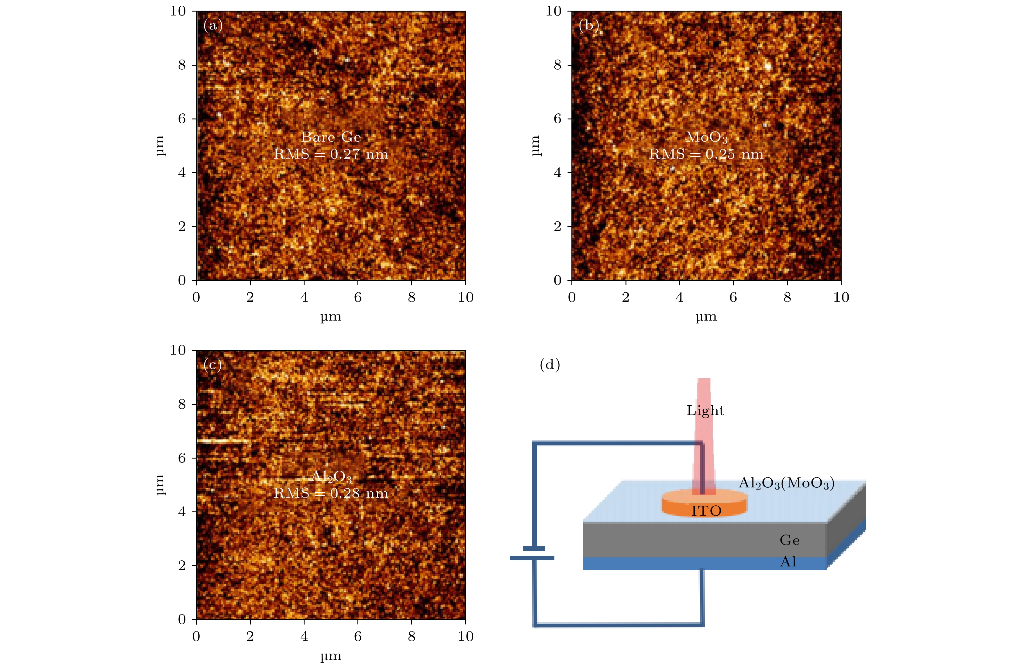
图 1 10 µm × 10 µm原子力显微镜图 (a) 本征锗表面; (b) MoO3(2 nm)/i-Ge; (c) Al2O3(2 nm)/i-Ge; (d) ITO/介质层/Ge光电探测器结构示意图
Figure 1. AFM images with a scanned area of 10 µm × 10 µm: (a) Bare i-Ge; (b) MoO3 (2 nm)/i-Ge; (c) Al2O3(2 nm)/i-Ge; (d) schematic illustration of the ITO/dielectric-layer/Ge photodetector.
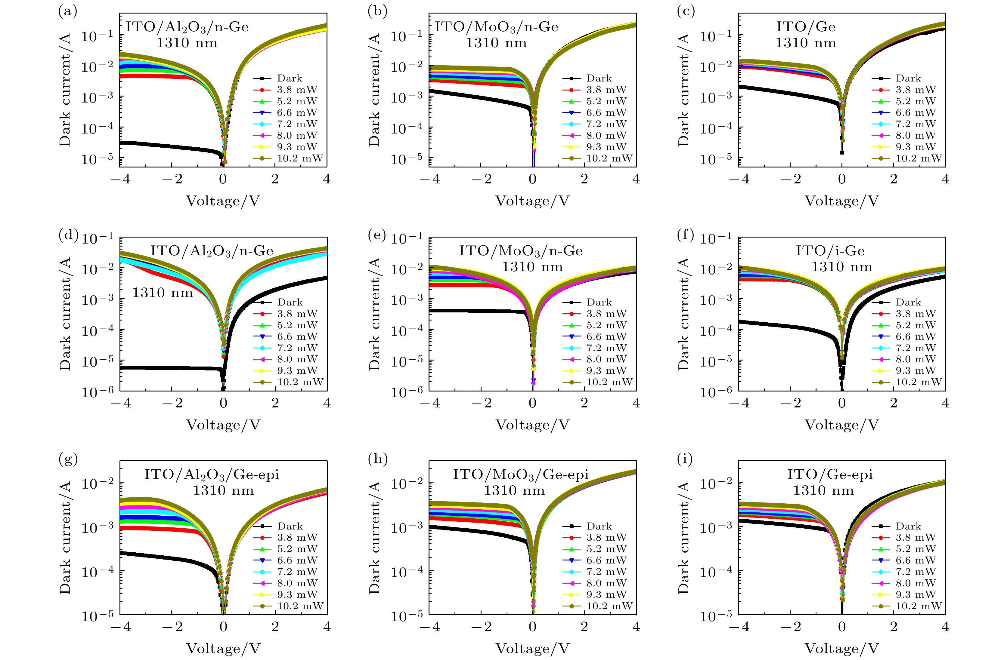
图 2 探测器在不同激光功率(1310 nm)照射下的I-V曲线与暗电流曲线对比 (a) ITO/Al2O3/n-Ge; (b) ITO/MoO3/n-Ge; (c) ITO/n-Ge; (d) ITO/Al2O3/i-Ge; (e) ITO/MoO3/i-Ge; (f) ITO/i-Ge; (g) ITO/Al2O3/Ge-epi; (h) ITO/MoO3/Ge-epi; (i) ITO/Ge-epi
Figure 2. Photocurrent and darkcurrent of the detectors measured under illumination by a 1310 nm laser at different powers: (a) ITO/Al2O3/n-Ge; (b) ITO/MoO3/n-Ge; (c) ITO/n-Ge; (d) ITO/Al2O3/i-Ge; (e) ITO/MoO3/i-Ge; (f) ITO/i-Ge; (g) ITO/Al2O3/Ge-epi; (h) ITO/MoO3/Ge-epi; (i) ITO/Ge-epi.
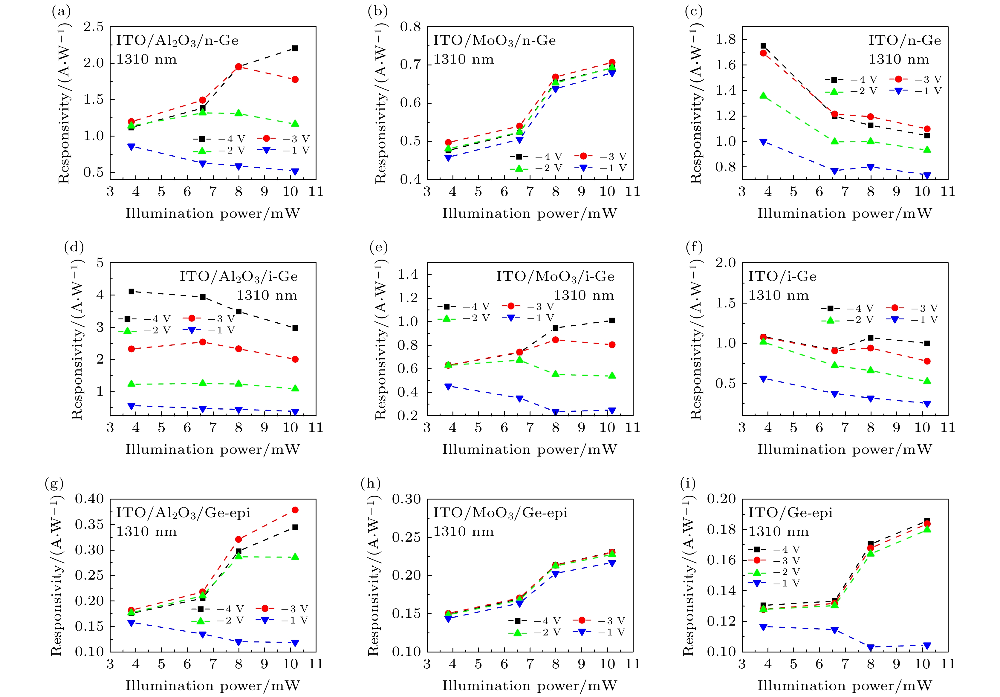
图 3 探测器在偏压为–1, –2, –3, –4 V、不同激光功率(1310 nm)照射下的响应度变化曲线 (a) ITO/Al2O3/n-Ge; (b) ITO/MoO3/n-Ge; (c) ITO/n-Ge; (d) ITO/Al2O3/i-Ge; (e) ITO/MoO3/i-Ge; (f) ITO/i-Ge; (g) ITO/Al2O3/Ge-epi; (h) ITO/MoO3/Ge-epi; (i) ITO/Ge-epi
Figure 3. Responsivities of the photodetectors measured at –1, –2, –3 and –4 V reverse bias under illumination by a 1310 nm laser at various powers: (a) ITO/Al2O3/n-Ge; (b)ITO/MoO3/n-Ge; (c) ITO/n-Ge; (d) ITO/Al2O3/i-Ge; (e) ITO/MoO3/i-Ge; (f) ITO/i-Ge; (g) ITO/Al2O3/Ge-epi; (h) ITO/MoO3/Ge-epi; (i) ITO/Ge-epi.
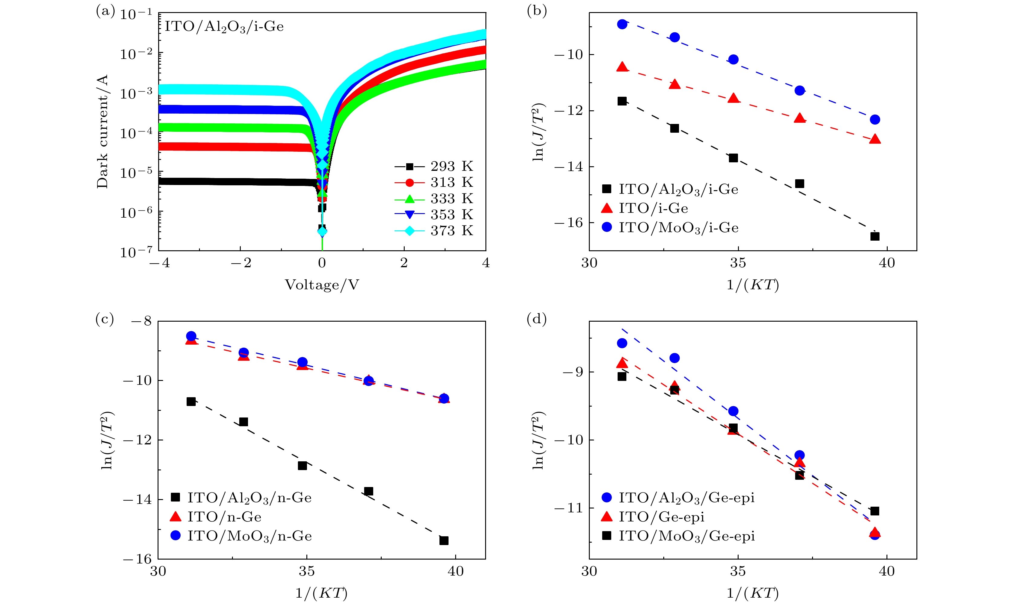
图 4 (a) ITO/Al2O3/i-Ge变温I-V曲线; (b) i-Ge组器件ln(J/T 2)与1/(kT)拟合结果; (c) n-Ge组器件ln(J/T 2)与1/(kT)拟合结果; (d) Ge-epi组器件ln(J/T 2)与1/(kT)拟合结果
Figure 4. (a) Temperature dependent I-V characteristics of ITO/Al2O3/i-Ge detector; (b) ln(J/T 2) versus 1/(kT) for i-Ge detectors; (c) ln(J/T 2) versus 1/(kT) for n-Ge detectors; (d) ln(J/T 2) versus 1/(kT) for Ge-epi detectors.

图 5 有效肖特基势垒高度与器件类型关系图
Figure 5. Diagram of effective Schottky barrier heights with device types.
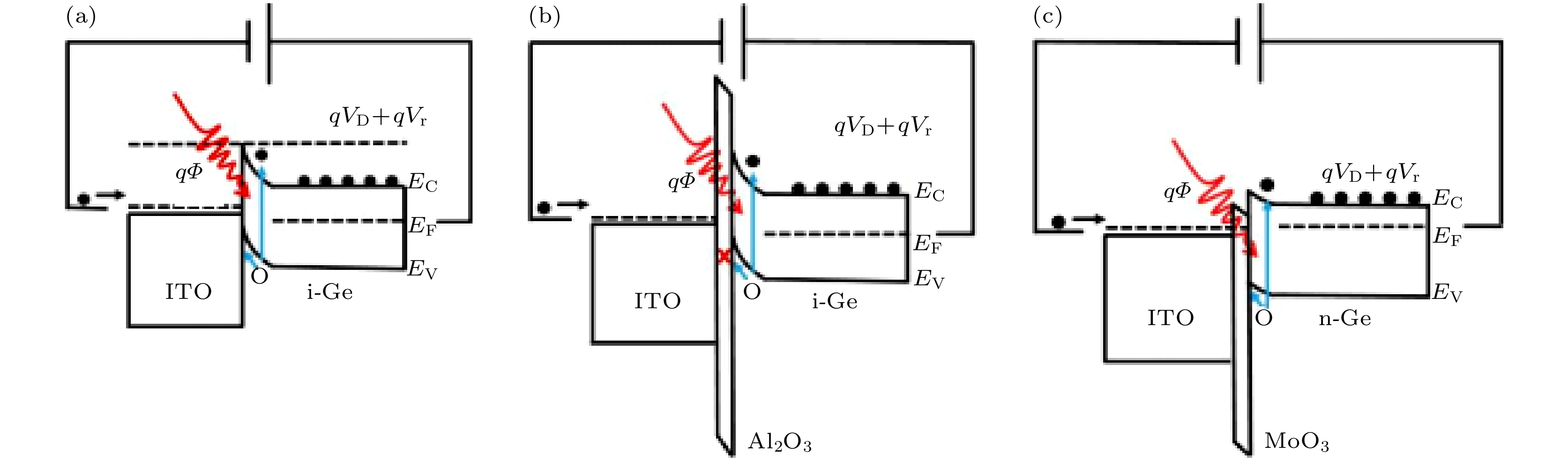
图 6 光照下探测器的能带结构图以及载流子输运示意图 (a) ITO/i-Ge; (b) ITO/Al2O3/i-Ge; (c) ITO/MoO3/n-Ge
Figure 6. Energy band and carrier transport diagram of detectors under light illumination: (a) ITO/i-Ge; (b) ITO/Al2O3/i-Ge; (c) ITO/MoO3/n-Ge.
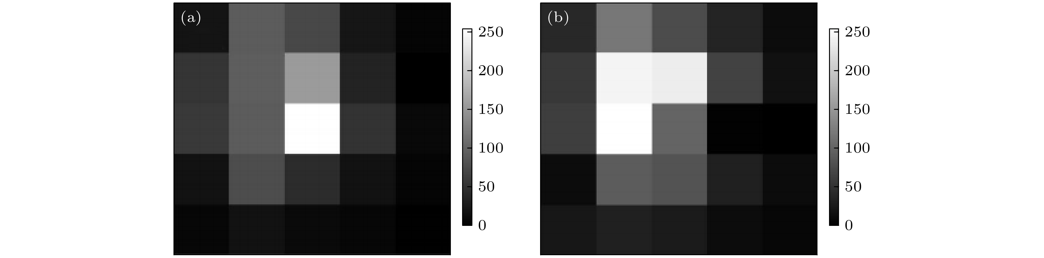
图 7 ITO/Al2O3/i-Ge二维成像图 (a) 1310 nm波长; (b) 1550 nm波长
Figure 7. Two dimensional image obtained from the ITO/Al2O3/i-Ge detector: (a) 1310 nm laser; (b) 1550 nm laser.
表 1 超薄介质插层调制的ITO/Ge肖特基光电探测器与文献报道的器件性能对比
Table 1. A comparison of the performance of our works with those from other groups.
年份 暗电流大小(密度) 响应度 结构类型 文献 2006 40 mA/cm2@1 V 0.28 A/W@1550 nm NI PIN [17] 2010 90 μA@1 V 0.14 A/W@1550 nm WG MSM [24] 2010 0.2 mA@–0.5 V 0.7 A/W@1550 nm WG PIN [25] 2011 40 mA/cm2@1 V 0.8 A/W@1500 nm WG Photodiode [26] 2013 412 μA@5 V 1.76 A/W@1550 nm WG MSM [27] 2015 3 nA@–1 V 1.0 A/W@1567 nm WG PIN [28] 2017 75 mA/cm2@1 V 0.58 A/W@1550 nm WG PIN [29] 2021 5.91 mA/cm2@–4 V 0.46 A/W@1550 nm
4.11 A/W@1310 nmNI MS 本文  DownLoad: CSV
表 2 不同结构的有效肖特基势垒高度
Table 2. Effective Schottky barrier heights of different structures.
结构类型 i-Ge n-Ge Ge-epi ITO 0.34 eV 0.24 eV 0.29 eV 2 nm Al2O3 + ITO 0.55 eV 0.56 eV 0.30 eV 2 nm MoO3 + ITO 0.39 eV 0.22 eV 0.25 eV
DownLoad: CSV
-
[1] Vivien L, Rouvière M, Fédéli J M, Marris-Morini D, Damlencourt J F, Mangeney J, Crozat P, Melhaoui L E, Cassan E, Le Roux X, Pascal D, Laval S 2007 Opt. Express 15 9843
Google Scholar
[2] Eng P C, Song S, Ping B 2015 Nanophotonics-Berlin 4 277
Google Scholar
[3] Soref R 1993 P. IEEE 81 1687
Google Scholar
[4] Soref R 2010 Nat. Photonics 4 495
Google Scholar
[5] Eng P C, Song S, Ping B 2010 Nat. Photonics 4 527
Google Scholar
[6] Wang J A, Lee S 2011 Sensors 11 696
Google Scholar
[7] Ahn D, Hong C Y, Liu F, Giziewicz W, Beals M, Kimerling L C, Michel J, Chen J, Kartner F X 2007 Opt. Express 15 3916
Google Scholar
[8] Kumar S, Chatterjee A, Selvaraja S K, Avasthi S 2020 IEEE Sens. J. 20 4660
Google Scholar
[9] 王兴军, 苏昭棠, 周治平 2015 中国科学: 物理学 力学 天文学 1 15
Wang X J, Su Z T, Zhou Z P 2015 Sci. Sin-Phys. Mech. Astron. 1 15
[10] Rogalski A 2003 Prog. Quant. Electron 27 59
Google Scholar
[11] Yu C Y, Huang Z W, Lin G Y, Mao Y C, Hong H Y, Zhang L, Zhao Y M, Wang J Y, Huang W, Chen S Y, Li C 2020 J. Phys. D 53 125103
Google Scholar
[12] Cui J S, Li T T, Yang F H, Cui W J, Chen H M 2021 Opt. Commun. 480 126467
Google Scholar
[13] Vivien L, Osmond J, Fedeli J M, Marris-Morini D, Crozat P, Damlencourt J F, Cassan E, Lecunff Y, Laval S 2009 Opt. Express 17 6252
Google Scholar
[14] Li X L, Liu Z, Peng L Z, Liu X Q, Wang N, Zhao Y, Zhen J, Zuo Y H, Xue C L, Cheng B W 2020 Chinese Phys. Lett. 37 038503
Google Scholar
[15] Fama S, Colace L, Masini G, Assanto G, Luan H C 2002 Appl. Phys. Lett. 81 586
Google Scholar
[16] Liu J F, Michel J, Giziewicz W, Pan D, Wada K, Cannon D D, Jongthammanurak S, Danielson D T, Kimerling L C, Chen J, Ilday F O, Kartner F X, Yasaitis J 2005 Appl. Phys. Lett. 87 103501
Google Scholar
[17] Huang Z H, Kong N, Guo X Y, Liu M G, Duan N, Beck A L, Banerjee S K, Campbell J C 2006 IEEE J. Sel. Top. Quantum Electron. 12 1450
Google Scholar
[18] Kang Y M, Liu H D, Morse M, Paniccia M J, Zadka M, Litski S, Sarid G, Pauchard A, Kuo Y H, Chen H W, Zaoui W S, Bowers J E, Beling A, McIntosh D C, Zheng X G, Campbell J C 2009 Nat. Photonics 3 59
Google Scholar
[19] Zhu H, Shan C X, Wang L K, Zheng J, Zhang J Y, Yao B, Shen D Z 2010 J. Phys. Chem. C 114 7169
Google Scholar
[20] Yu J, Shan C X, Qiao Q, Xie X H, Wang S P, Zhang Z Z, Shen D Z 2012 Sensors 12 1280
Google Scholar
[21] Huang Z W, Yu C Y, Chang A L, Zhao Y M, Huang W, Chen S Y, Li C 2020 J. Mater. Sci. 55 8630
Google Scholar
[22] Mazur M, Pastuszek R, Wojcieszak D, Kaczmarek D, Lubanska A https://www.emerald.com/insight/content/doi/10.1108/CW-11-2019-0170/full/html [2020-12-07]
[23] Huang Z W, Mao Y C, Lin G Y, Yi X H, Chang A L, Li C, Chen S Y, Huang W, Wang J Y 2018 Opt. Express 26 5827
Google Scholar
[24] Assefa S, Fengnian X, Vlasov Y A 2010 In Proceedings of Optical Fiber Communication Conference and Exposition and the National Fiber Optic Engineers Conference Los Angeles, CA USA, March 21−25, 2010 p1
[25] Feng N N, Dong P, Zheng D W, Liao S R, Liang H, Shafiiha R, Feng D Z, Li G L, Cunningham J E, Krishnamoorthy A V, Asghari M 2010 Opt. Express 18 96
Google Scholar
[26] DeRose C T, Trotter D C, Zortman W A, Starbuck A L, Fisher M, Watts M R, Davids P S 2011 Opt. Express 19 24897
Google Scholar
[27] Harris N C, Baehr-Jones T, Lim A E J, Liow T Y, Lo G Q, Hochberg M 2013 J. Lightwave Technol. 31 23
Google Scholar
[28] Chen H T, Verheyen P, De Heyn P, Lepage G, De Coster J, Absil P, Roelkens G, Van Campenhout J 2015 J. Lightwave Technol. 33 820
Google Scholar
[29] 王尘, 许怡红, 李成, 林海军 2017 物理学报 66 198502
Google Scholar
Wang C, Xu Y H, Li C, Lin H J 2017 Acta Phys. Sin. 66 198502
Google Scholar
[30] Tong Y, Liu B, Lim P S Y, Yeo Y C 2012 IEEE Electron Device Lett. 33 773
Google Scholar
[31] Manik P P, Lodha S 2015 Appl. Phys. Express 8 051302
Google Scholar
[32] Robertson j 2000 J. Vac. Sci. Technol. B 18 1785
Google Scholar
[33] Zheng S, Yang W, Sun Q Q, Chen L, Zhou P, Wang P F, Zhang D W, Xiao F 2013 Appl. Phys. Lett. 103 261602
[34] Irfan I, Turinske A J, Bao Z N, Gao Y L 2012 Appl. Phys. Lett. 101 093305
Google Scholar
[35] 韩百超, 高明, 陈东运, 宋文磊, 宋晓敏, 徐飞, 赵磊, 马忠权, 张志恒, 莫镜辉 2017 第一届全国功能薄膜与涂层学术研讨会暨国际论坛 中国昆明 2017-07-23 p2
Han B C, Gao M, Chen D Y, Song W L, Song X M, Xu F, Zhao L, Ma Z Q, Zhang Z H, Mo J H 2017 Summary of the First National Symposium on Functional Films and Coatings and International Forums Kun Ming, China, July 23, 2017 p2 (in Chinese)

 DownLoad:
Catalog
Metrics
- Abstract views: 4555
- PDF Downloads: 96
- Cited By: 0
