


SPECIAL TOPIC—Thermoelectric materials and applied physics

2021, 70 (20): 206501.
doi: 10.7498/aps.70.20211050
Abstract +
Thermoelectric materials, a kind of new energy material, can directly convert heat energy into electric energy, and vice versa, without needing any other energy conversion. However, the present development status of thermoelectric materials severely restricts their engineering applications in thermoelectric devices. Improving the thermoelectric performances of existing thermoelectric materials and exploring new thermoelectric materials with excellent performance are eternal research topics in thermoelectricity field. In recent years, the MAX phases and their derived MXene phases have gradually received the attention of researchers due to their unique microstructures and properties. The crystal structure of MAX phases is comprised of Mn+1Xn structural units and the single atomic plane of A stacked alternately. The two-dimensional MXene phase derived can be prepared after the atoms in the A-layer of MAX have been etched. The MAX phases and their derived MXene phases have both metal feature and ceramic feature, and also have good thermal conductivity and electric conductivity, and they are anticipated to be the promising thermoelectric materials. In this paper, the present development status of the preparation technology and the thermoelectric properties of MAX phases and MXene are reviewed. Finally, some feasible schemes to improve the thermoelectric properties of MAX and its derived MXene phase materials are proposed, and the development direction and prospect of MAX phases and MXene are prospected as well.
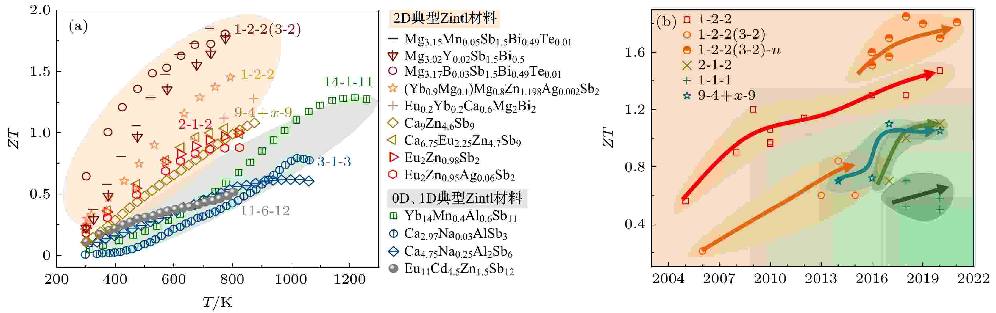
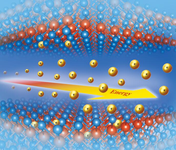
Research progress of two-dimensional covalent bond substructure Zintl phase thermoelectric materials
2021, 70 (20): 207304.
doi: 10.7498/aps.70.20211010
Abstract +
Thermoelectric materials can realize the direct conversion between thermal energy and electrical energy, and thus having important applications in semiconductor refrigeration and heat recovery. Zintl phase is composed of highly electronegative cations and anions, which accords with the concept of “phonon glass, electron crystal” (PGEC). Thermoelectric properties of Zintl phase have attracted extensive interest, among which the two-dimensional (2D) covalent bond structure featured Zintl phases have received more attention for their outstanding electrical properties. In this review, Zintl phase materials with two-dimensional covalent bond substructures are reviewed, including 1-2-2-type, 9–4+x–9-type, 2-1-2-type and 1-1-1-type Zintl phase. The 1-2-2-type Zintl phase is currently the most widely studied and best-performing Zintl material. It is worth mentioning that the maximum ZT value for the Mg3Sb2-based n-type Zintl material with the CaAl2Si2 structure has been reported to reach 1.85, and the average ZT value near room temperature area also reaches 1.4. The 9–4+x–9-type Zintl material with a mass of atoms in unit cell contributes to lower thermal conductivity thus relatively high ZT value. The 2-1-2-type Zintl material has extremely low thermal conductivity due to the intrinsic vacancies, which has been developing in recent years. The 1-1-1-type Zintl material with the same ZrBeSi structure as the 2-1-2-type Zintl material, shows better electrical transport performance. In sum, this review summarizes the recent progress and optimization methods of those typical Zintl phases above. Meanwhile, the future optimization and development of Zintl phase with two-dimensional covalent bond substructures are also prospected.
2021, 70 (20): 207101.
doi: 10.7498/aps.70.20211165
Abstract +
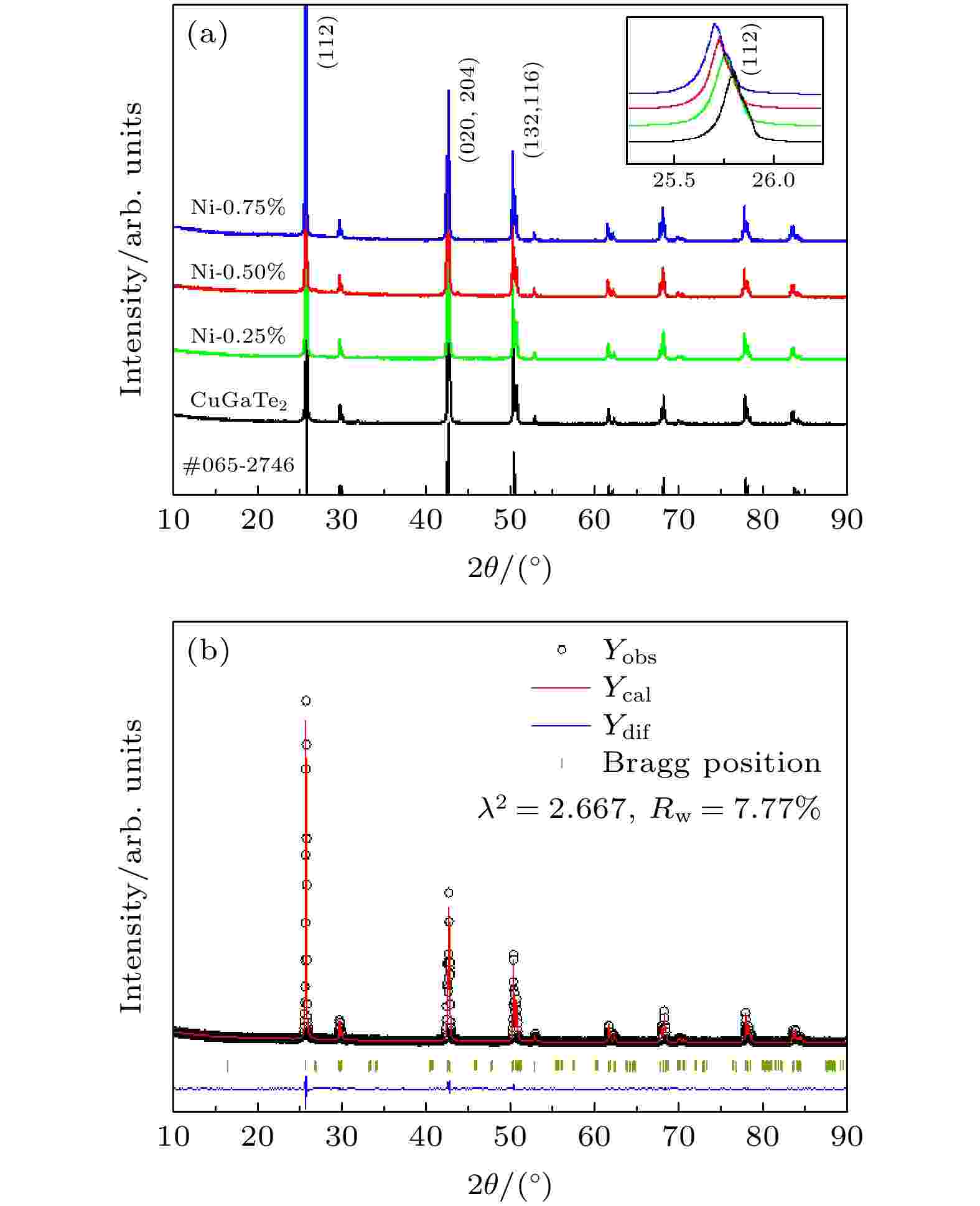
Thermoelectric material is a new type of functional material that can realize the direct conversion between heat energy and electric energy. It has received a lot of attention because it has wide practical applications. However, the applications of thermoelectric devices are limited by their low conversion efficiencies. The conversion efficiency is determined mainly by the thermoelectric properties of the material. In this work, a compound of CuGaTe2 chalcopyrite is selected as a research object, and a series of Ni-doped samples Cu1–xNixGaTe2 (x = 0–0.75%) is synthesized by the vacuum melting method. The temperature dependent thermal and electrical properties for Cu1–xNixGaTe2 (x = 0–0.75%) compounds are investigated. The results show that the Ni atom can effectively replace the Cu atom of the material, and thus leading the carrier concentration to decrease slightly and inducing the mobility to increase. At the same time, the Seebeck coefficient increases significantly after Ni doping: on the one hand, the increase is due to the decrease of the carrier concentration of the sample; on the other hand, the effective increase of the density of states near the Fermi level plays an important role in increasing Seebeck coefficient. Then, the thermal conductivity decreases effectively due to the enhancement of point defect scattering caused by Ni doping, and the minimum lattice thermal conductivity is reduced by ~30% in comparison with the matrix lattice thermal conductivity. Finally, the maximum ZT value for Cu0.095Ni0.005GaTe2 sample (ZT = 1.26 at 873 K) is obtained to be ~56% larger than that for CuGaTe2. This work indicates that the doping magnetic element Ni at Cu site is also one of the effective ways to improve the thermoelectric properties of CuGaTe2 materials.
COVER ARTICLE
2021, 70 (20): 207303.
doi: 10.7498/aps.70.20211090
Abstract +
Bi2Te3-based alloys have been long regarded as the materials chosen for room temperature thermoelectric (TE) applications. With superior TE performances, Bi2Te3-based bulk materials have been commercially used to fabricate TE devices already. However, bulk materials are less suitable for the requirements for applications of flexible or thin film TE devices, and therefore the thin film materials with advanced TE properties are highly demanded. Comparing with bulk materials and P-type Bi2Te3-based thin films, the TE properties of N-type Bi2Te3-based thin films have been relatively poor so far and need further improving for practical applications. In this study, a series of N-type Bi2Te3–xSex thin films is prepared via magnetron sputtering method, and their structures can be precisely controlled by adjusting the sputtering conditions. Preferential layered growth of the Bi2Te3–xSex thin films along the (00l) direction is achieved by adjusting the substrate temperature and working pressure. Superior electrical conductivity over 105 S/m is achieved by virtue of high in-plane mobility. combining the advanced Seebeck coefficient of Bi2Te3-based material with superior electrical conductivity of highly oriented Bi2Te3–
2021, 70 (20): 208401.
doi: 10.7498/aps.70.20211444
Abstract +
SnSe, a layered material with intrinsic low thermal conductivity, is reported to have excellent thermoelectric properties. SnSe2 has a similar structure to SnSe, but the SnSe2 has a low electrical transport, resulting in a poor thermoelectric performance, and the intrinsic SnSe2 has a maximum ZT value of only ~ 0.09 at 773 K. In this work, SnSe1.98Br0.02-y%Cu (y = 0, 0.50, 0.75, 1.0) bulk materials are synthesized by the melting method combined with spark plasma sintering (SPS) based on the carrier concentration improved through Br doping. In the SnSe2 materials with van der Waals chemical bonding between layers, the synergistic effects of intercalating Cu on the thermoelectric properties are investigated. On the one hand, the extra Cu not only provides additional electrons but also can be embedded stably in the van der Waals gap and form an intercalated structure, which is beneficial to the charge transfer in or out of the layers, and thus synergistically improving the carrier concentration and carrier mobility. On the other hand, owing to the dynamic Cu doping, the increase of carrier concentration compensates for the decrease of carrier mobility caused by carrier-carrier scattering, which maintains the high electrical transport properties at high temperature. The present results show that at room temperature, the power factors along the parallel and perpendicular to the SPS (//P and ⊥P) sintering directions increase from ~0.65 and ~0.98 µW·cm–1·K–2 for intrinsic SnSe2 to ~10 and ~19 μW·cm–1·K–2 for SnSe1.98Br0.02-0.75%Cu samples, respectively. Finally, at 773 K, the maximum ZT value of ~0.8 is achieved along the ⊥P direction. This study proves that the SnSe2 greatly promises to become an excellent thermoelectric material.
REVIEW
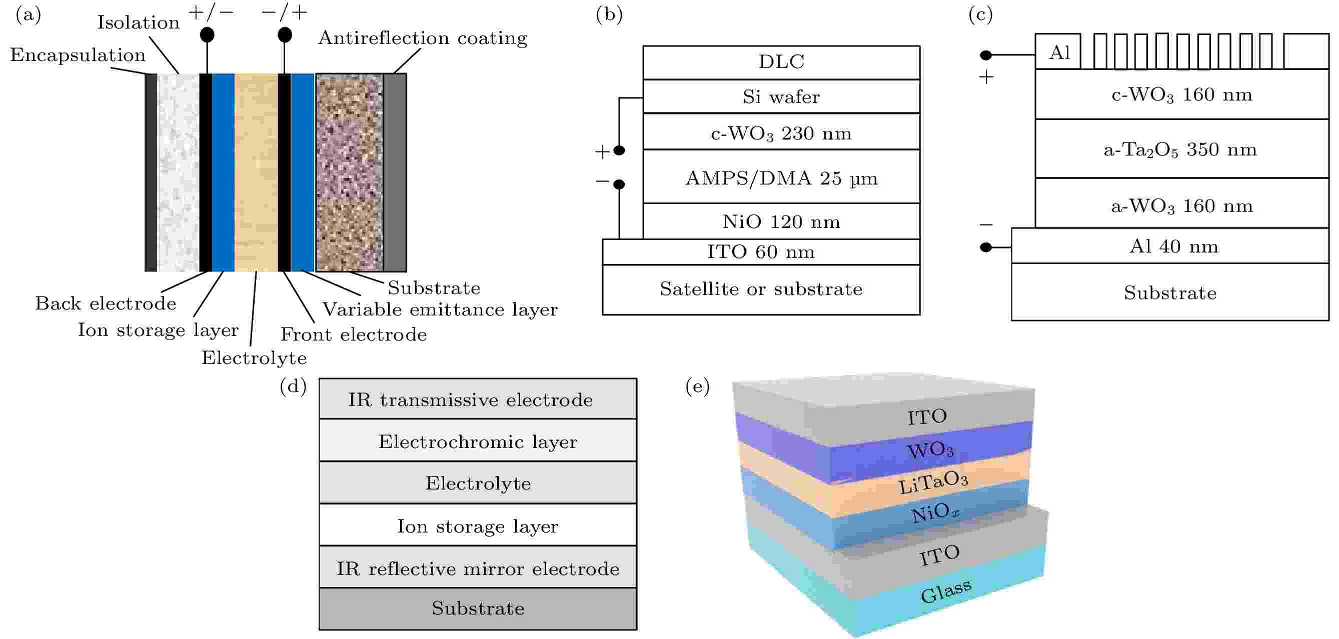
2021, 70 (20): 204205.
doi: 10.7498/aps.70.20210211
Abstract +
Infrared electrochromic device is a kind of device whose infrared emissivity can change reversibly under electric field excitation. This kind of device has important applications in the fields of adaptive infrared camouflage and intelligent thermal control, and has become a research frontier and hot spot in the field of infrared radiation control. In this paper, the working principle, research status and progress of infrared electrochromic devices based on metal oxides, conductive polymers, graphene and metals are summarized, and the development trend of infrared electrochromic device is analyzed.
2021, 70 (20): 207302.
doi: 10.7498/aps.70.20210675
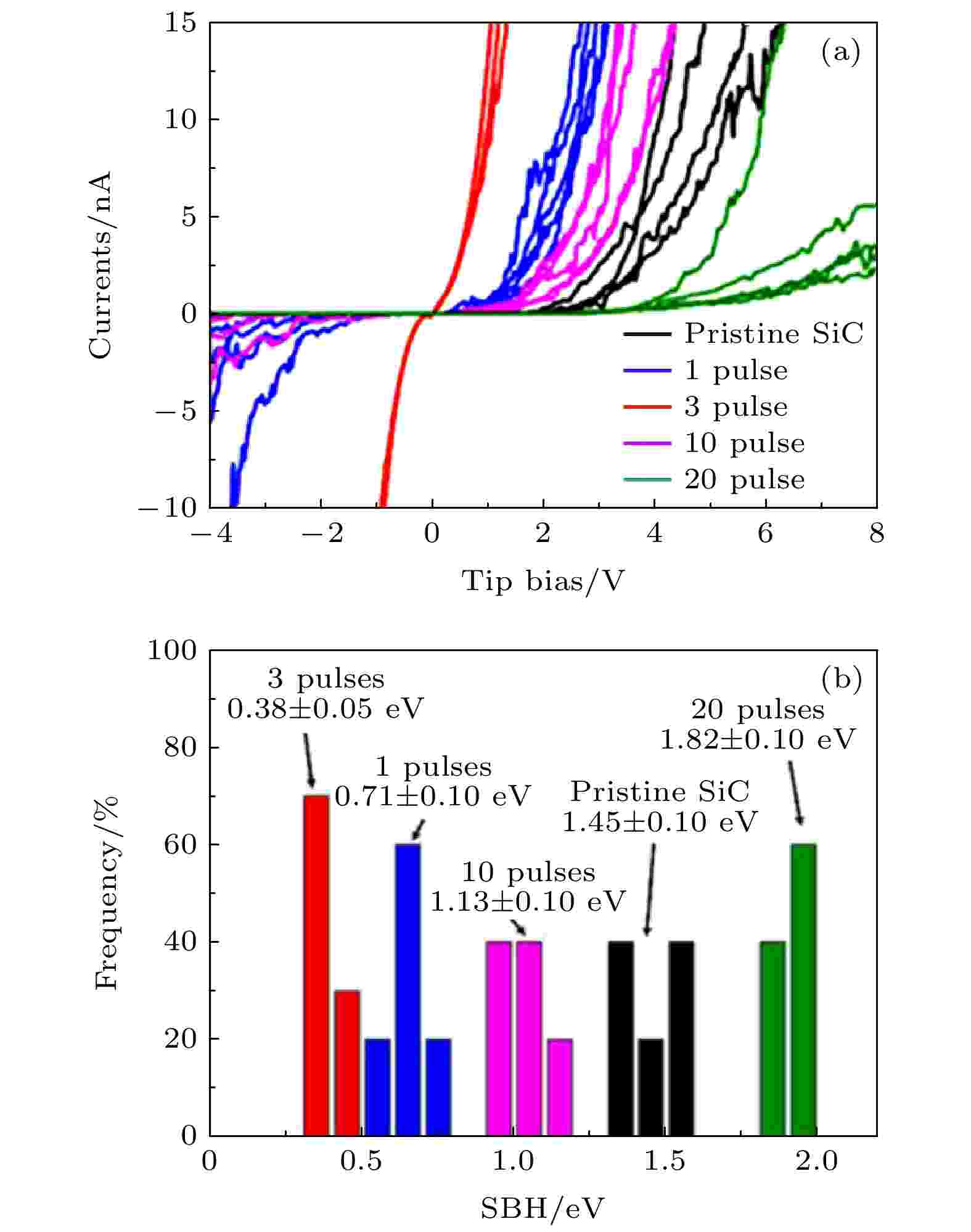
Abstract +
Silicon carbide (SiC) is a promising candidate for applications in high temperature, high voltage, high power, and low-power dissipation devices due to its unique properties like wide band gap, high critical electric field, and high thermal conductivity. However, one of the main bottlenecks hindering the SiC power devices from developing and being put into practical application is the fabrication of good metal/SiC contact. In this review, the research status of Ohmic contact and Schottky contact of SiC device are compared and analyzed. The complicated interface properties and uncontrollable barrier height at metal/SiC interface are revealed. In addition, the research status of metal/SiC contact barrier and interface state properties are analyzed, and the important significance of effective control of interface barrier is highlighted. Furthermore, the research progress of metal/SiC contact interface regulation technology is specially analyzed. The future development directions in the nature of metal/SiC interface states and interface control technology are finally prospected.
GENERAL
2021, 70 (20): 200201.
doi: 10.7498/aps.70.20210640
Abstract +
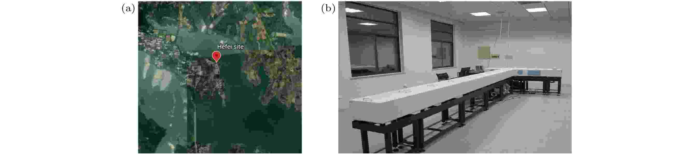
Atmospheric dichlorodifluoromethane (CCl2F2, CFC-12), as a synthetic chemical agent, is a main stratospheric ozone-depleting substance in atmosphere. Studies of the detection techniques and the temporal and spatial distribution of CFC-12 have great significance in understanding the variation trend of regional CFCs and their influence on stratospheric ozone. In this study, the method of retrieving the vertical profile and total column for CFC-12 is studied based on ground-based high-resolution Fourier transform infrared spectroscopy (FTIR). The spectral window for CFC-12 retrieval is selected as 922.5–923.6 cm–1, where the interfering gases are H2O, O3, and CO2. The result of error analysis shows that the average total error is 1.27%, including the systematic error 0.76% and random error 1.02%. The vertical profiles and total columns of atmospheric CFC-12 in Hefei during the period from 2017 to 2020 were retrieved based on the optimal estimation algorithm. The vertical profiles of CFC-12 show that the concentration of atmospheric CFC-12 is high in the troposphere and low stratosphere at the altitude of 0–20 km, and then decreases, very low at height above 40 km. The total column average kernel of retrieved CFC-12 profiles is higher at 15–20 km, and the typical signal degree of freedom of CFC-12 is 1.217. Moreover, the long-term total columns of atmosphere CFC-12 observed show obvious seasonal variation in Hefei. Total columns of atmosphere CFC-12 are higher in summer and lower in winter and early spring. The maximum monthly concentration of CFC-12 is about 1.13 × 10¹⁶ mol·cm–2 in July, and the minimum monthly concentration is 1.00 × 10¹⁶ mol·cm–2 in March. Also, the annual average total columns of atmospheric CFC-12 decreased slightly from 2017 to 2020, with an increasing rate of –0.68%. This reflects the effect of China's implementation of CFCs control ban policy. Furthermore, in order to verify the accuracy of ground-based FTIR observation, we compare our ground-based observation data with ACE-FTS/ SCISAT satellite version 4.1 level 2 data. There are 16 pairs of matching points between satellite observation and ground observation data, and the correlation coefficient is 0.73 for two CFC-12 partial columns at the height of 16–28 km, showing good agreement between ground-based FTIR data and satellite data. The long-term observations demonstrate the accuracy and reliability of ground-based high-resolution FTIR technology for detecting the vertical distribution and seasonal variation of atmosphere CFC-12.
2021, 70 (20): 200202.
doi: 10.7498/aps.70.20210905
Abstract +
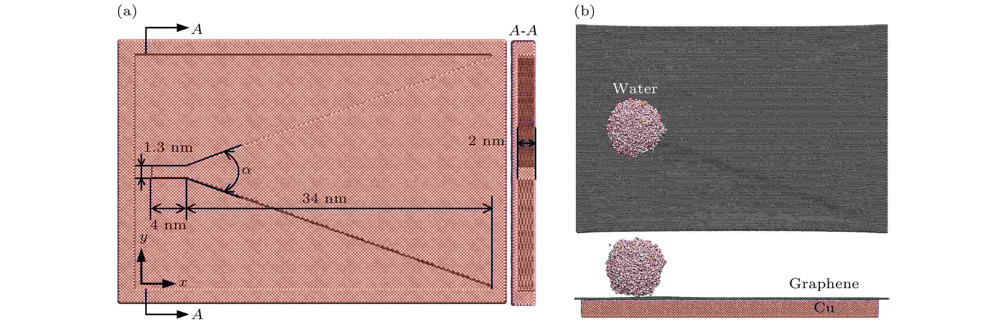
The self-driving of water droplets on textured substrate is momentous for understanding the directional transport of water on biological surface. In this paper, a novel design of monolayer graphene-covered wedge-shaped copper substrate (GWCS) is put forward to realize the directional and ultrafast spontaneous driving of water droplets from the tip of the wedge-shaped substrate to the wide end. The self-driving behaviors of water droplets on GWCS are studied by classical molecular dynamics. The results show that the maximum spontaneous driving velocity of water droplet driven by surface wetting gradient and Young-Laplace pressure gradient can reach 73.8 m/s. The law of energy variation during the whole droplet self-driving on GWCS indicates that there is a competitive relationship between the potential energy of water droplet and the interaction energy between the droplet and GWCS, i.e. the interaction energy between water droplet and GWCS is partially converted into the potential energy of water droplet. The relationship of the maximum displacement of water droplet with the wedge angle, wettability of GWCS and the droplet surface tension is proposed in theory, and the influence of the discontinuous linear increase of the wedge-shaped substrate width on a nanoscale on the self-driving is analyzed and used to explain the little difference between the theoretical and simulation results. Furthermore, a smaller droplet is easier to obtain larger spontaneous driving velocity, and the influence of long-distance decelerating motion of high-speed small droplet on the non-wetting gradient substrate on the droplet displacement law is clarified. Finally, the mechanism of graphene suspended on both sides of the wedge-shaped copper structure to enhance the droplet transport efficiency is determined. The results will have theoretical significance in designing the functional texture surface covered by monolayer graphene to realize droplet self-driving.
2021, 70 (20): 200301.
doi: 10.7498/aps.70.20210092
Abstract +
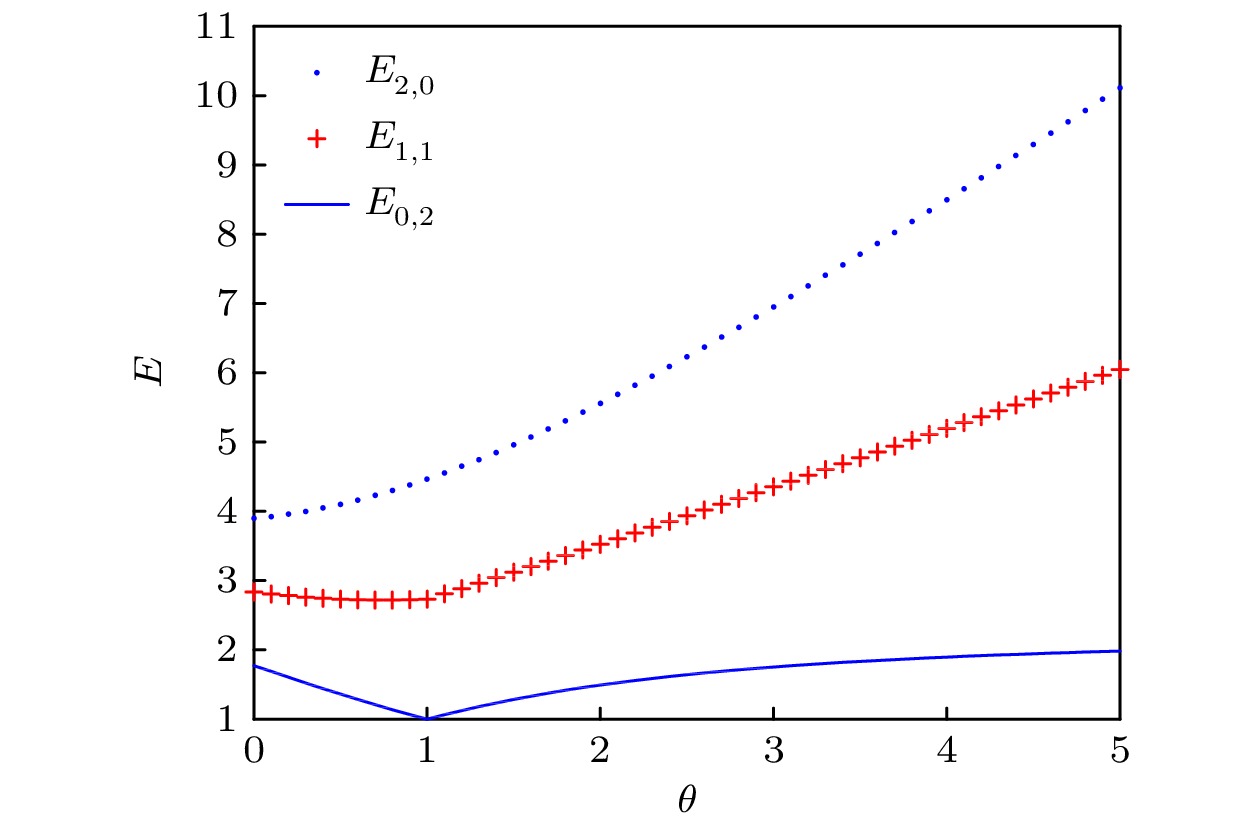
The ideas of noncommutative space originate from the research on time-space coordinate on an extremely small scale. Subsequently, the noncommutative space has gradually attracted some attention. The researchers started to explore noncommutative effect in some other fields. With the establishment of noncommutative quantum mechanics, it becomes significant to explore the noncommutative effect of exactly solvable models. The kinds of harmonic oscillators are very important and fundamental models in physics. But in noncommutative phase space, coordinate and coordinate are noncommutative, and momentum and momentum are also noncommutative. These results in the difficulty in obtaining the energy spectra of oscillators systems. In this paper the quantum properties of a two-dimensional coupling harmonic oscillator in noncommutative phase space are studied. Firstly, the Hamiltonian of the system is constructed, which includes all possible coupling types, namely, coordinate-coordinate coupling, momentum-momentum coupling, and coordinate-momentum cross-coupling. Secondly, the explicit expression of the noncommutative energy spectrum for the Hamiltonian is obtained by using the invariant eigen-operator method. In this work it is shown explicitly that the changes in the energy levels are related to the noncommutative parameters and coupling parameters. Thirdly, the effects of coupling parameters and non-commutative parameters on the energy spectra are analyzed in detail in the form of graphs. The results show that the energy levels under the influence of non-commutative parameters are non-degenerated. As the values of non-commutation parameters $ \theta $ and $ \phi $ increase, some energy levels increase and tend to change linearly, and other energy levels first decrease and then increase. If the limit values of the non-commutative parameters are taken as follows: $ \theta \to 0 $ and $ \phi \to 0 $ , then the noncommutative energy spectra will be consistent with the energy spectra of the two-dimensional harmonic oscillator in the commutative space in general. On the other hand, the energy levels will split under the influence of coupling parameters. Moreover, the degree to which the energy levels split can increase as the kinds of couplings in the system increase. It is found that the coordinate coupling parameter $ \eta $ and the momentum coupling parameter $ \sigma $ have the same influence on the energy levels, but the coordinate momentum cross-coupling parameter $ \kappa $ has less influence on the energy levels than $ \eta $ and $ \sigma $ . Overall, the above results are completely different from those of two-dimensional oscillator in the usual commutative space, which is degenerated except for the ground state.


EDITOR'S SUGGESTION
2021, 70 (20): 200302.
doi: 10.7498/aps.70.20210705
Abstract +
NUCLEAR PHYSICS
2021, 70 (20): 202901.
doi: 10.7498/aps.70.20210891
Abstract +
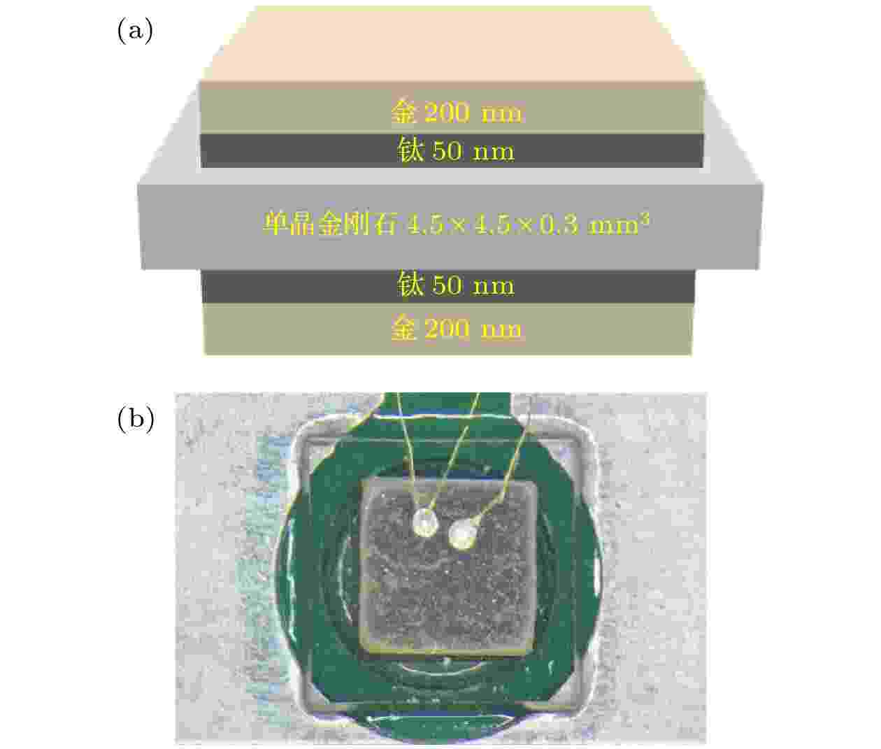
Single-crystal diamond (SCD) detectors promise to have applications in neutron spectrometers and fusion neutron monitoring under high flux deuterium plasma. The response to 14 MeV neutrons for the SCD detector is studied in this paper. A high-performance SCD neutron detector is developed by processing cleaning wafer, depositing metal electrodes, annealing and wire-bonding. A fast-neutrons monitoring system containing the detector, preamplifier and digital multichannel analyzer is constructed, and the response to 14 MeV neutrons for the detector is measured on the K-400 neutron generator supported by China Academy of Engineering Physics. In addition, computational simulations of the energy deposition and detection efficiency of 14 MeV neutron through diamond are performed via Geant4 toolkit based on evaluated nuclear data libraries of ENDF-VIII.0, JEFF-3.3, BROND-3.1, JENDL-4.0u and CENDL-3.1. The methods of widening the simulation spectrum and calibration of measuring spectrum are presented in order that simulation results are in reasonable agreement with measured values. The results indicate that the energy deposition of 14 MeV neutrons incident on the 12C can be more accurately calculated with CENDL-3.1 than with other data libraries. The elastic scattering and reaction of 12C(n, 3α) are described more accurately with the CENDL-3.1, and the characteristic peaks of 12C(n, α)9Be matched well the calibrated testing spectrum and the after-widening simulation spectrum, with a difference between the simulated detection efficiency and measuring results being as low as 0.61%. The outcome measures are described as the standardized mean difference, with a detection efficiency of (3.31 × 10⁻⁴ ± 0.11 × 10⁻⁴) counts/n, an energy resolution of 4.02% ± 0.09%, and a peaking channel of 1797.24 ± 0.80, which suggest that the detector keeps stable well under a high neutron flux of 2 × 10¹⁰ n/s for as long as 2 h. The results demonstrate that the SCD detector can be a promising candidate for monitoring 14 MeV D-T neutrons.
ATOMIC AND MOLECULAR PHYSICS
2021, 70 (20): 203301.
doi: 10.7498/aps.70.20210670
Abstract +
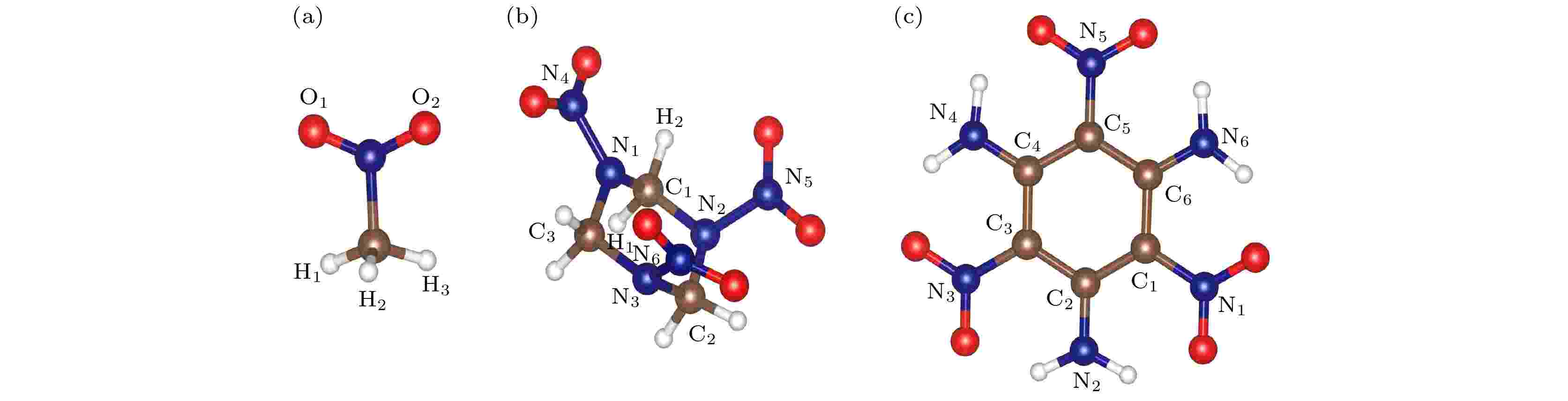
Nitro explosive is a main type of energetic material which can release a large amount of energy when detonated under extreme conditions. Further study of the excited state dynamics of photo-induced nitro explosive can provide an effective method to understand the complex process of ultrafast detonation physics. In this paper, the initial step of photodissociation at the first excited electron state of some typical nitro explosives including nitromethane (NM), cyclotrimethylenetrinitramine (RDX) and triaminotrinitrobenzene (TATB) is studied using the time-dependent density functional theory and the molecular dynamic method. The transient structures of energetic molecules and time evolutions of excited energy levels are observed. It is found that the structural relaxation of energetic molecules occurs immediately after the electronic excitation, and the entire photoexcitation process comes into being within a range of 200 fs. At the same time, the positions of molecular energy levels change to various degrees with the oscillations of different frequencies, such as the overlap between HOMO and LUMO, which is related to the obvious change of molecular configuration, indicating that the energy of excited carriers transfers to atoms in the form of heat through electron-phonon coupling, and the energy is redistributed through vibration relaxation in the initial stage of photodissociation which causes the chemical bonds of C—H, N—N and N—N to rupture, and the hydrogen atoms dissociated from methyl, methylene or amino groups, and the nearest nitro group to form some new intermediate states. In this process, the energy levels near the excited electron and hole energy also change significantly with time, suggesting that the coupling between electron and electron also plays a role in the dissociation process. Comparing with NM and RDX, the evolution of the excited energy level of TATB has obvious lower-frequency (phonon frequency) oscillations, showing that the coupling between electronic state and phonon of TATB is weak and thus makes it more difficult to dissociate. Our study can deepen the understanding of the structural relaxation of excited states and the time evolution of excitation energy levels in energetic materials, and provide a new understanding of the photoinduced reaction and the initial steps of laser ignition in energetic materials.
ELECTROMAGNETISM, OPTICS, ACOUSTICS, HEAT TRANSFER, CLASSICAL MECHANICS, AND FLUID DYNAMICS
2021, 70 (20): 204101.
doi: 10.7498/aps.70.20210309
Abstract +
Radiation power of an electromagnetic wave plays a decisive role in its transmission distance. Traditionally, the radiation power can be improved by expanding the radiation aperture size of the antenna array or increasing input power of the unit cell. However, the radiation aperture size is always restricted by assembly space. The input power improvement of the unit cell is always limited by the signal source. It is difficult to improve radiation power on a finite radiation aperture. However, the radiation power on a finite radiation aperture is related closely to the number of antenna elements and the radiation efficiency of the antenna array. It is useful to arrange more elements and improve radiation efficiency of the antenna array to improve the radiation power on a finite radiation aperture. Wideband wide-angle scanning phased array is able to make full use of a finite radiation aperture. The wide-angle scanning properties make it possible for the radiated power to cover a wide area. In this paper, a compact wideband wide-angle scanning tightly coupled dipole array (TCDA) is proposed. A high permittivity substrate and compact wideband balun are used for miniaturizing the antenna array. The period of the unit cell is only 0.144λhigh × 0.144λhigh (λhigh is the wavelength at the highest operation frequency in free space). Parameters of the balun are optimized to improve impedance matching between the balun and the antenna array. Two bilateral frequency selective surfaces (FSSs) are used to replace traditional dielectric superstrate to improve the impedance matching between the antenna array and free space. A low-loss dielectric substrate is used to reduce dielectric loss of the antenna array. In these ways, the radiation efficiency is greatly improved. The simulation results show that the proposed antenna array operates at 1.7–5.4 GHz (3.2:1) while scanning up to 65° in the E plane, 45° in the H plane and 60° in the D plane with following a rigorous impedance matching criterion (active VSWR < 2). A 16 × 16 prototype array is fabricated and measured. Good agreement is achieved between the simulation results and the measurement results. Compared with the designs in the literature, the proposed antenna array has an excellent performance in radiation power on a finite radiation aperture.
2021, 70 (20): 204201.
doi: 10.7498/aps.70.20210691
Abstract +
Compared with infrared laser sources, the three-dimensional incoherent extended light source has the advantages of high power, wide spectral range, and low cost. It has extremely wide applications in high-precision and multi-component photoacoustic spectrometers. However, it encounters some problems about poor directivity, low energy density, irregular shape, light field shaping needed in the design of optical system. The photoacoustic spectrometer is required to collect and optimize the radiation of the centimeter-level three-dimensional extended light source to the whole space in a small volume. Through using a series of wavelength and frequency modulation elements, the final cylindrical light field distribution with millimeter-level radius and centimeter-level length is realized. According to the concept of optical expansion and the principle of edge light, this paper breaks through the traditional design mode based on point light source in the process of optical system design and optimization. The concept of extended light source is used throughout the design process. The luminous characteristics of the three-dimensional extended light source are directly acquired by the self-designed measurement method and device which is accurately reflected in the three-dimensional extended light source model in the form of micro-element. The design of the light field shaping system of the three-dimensional extended light source for the photoacoustic spectrometer is realized by the aspheric surface, and the relevant experimental verification is carried out. Taking the Hawkeye IR-Si272 light source for example, the experimental value of the light power at the entrance of the photoacoustic cell and the sidewall noise rate of the photoacoustic spectrometer have a small deviation from their corresponding simulation values. Compared with the original condenser system, the self-designed photoacoustic spectrometer light source system increases the value of the light power at the entrance of the photoacoustic cell from 0.86W to 1.32W, and reduces the value of the sidewall noise rate from 50.3% to 19.7%. The lower limit of detection of the concentration of trace gas in the order of ppm (parts per million) is also achieved.
EDITOR'S SUGGESTION
2021, 70 (20): 204202.
doi: 10.7498/aps.70.20210234
Abstract +
Quantum noise has become an important limiting factor in the application of precision measurement, and its relevant problems have become a research hotspot. As an important optical device to manipulate quantum noise, the optical resonator possesses the transmission characteristics that determine the evolution characteristics of output signal’s noise. According to their impedance matching factor a values, the resonators can be divided into three categories: over-coupled cavity for $a \in [ - 1, 0)$ , impedance matched cavity for $a{{ = }}0$ , and under-coupled cavity for $a \in (0, 1]$ . When the resonator fully meets the resonant conditions, its output field can be regarded as a low-pass filter, the high-frequency noise is directly reflected. The high-frequency noise at the output end is greatly suppressed, and the noise at the frequency far larger than the linewidth reaches the shot noise standard. Therefore, the noise of the optical field beyond the linewidth range can be greatly suppressed by the narrow linewidth optical resonator. At the same time, from the three kinds of optical resonator phase diagrams it can be found that the over-coupled cavity is in a state of half a detuning and the sideband frequency phase rotates ± 90° relative to the carrier frequency. In this case, the phase noise of light field can be converted into amplitude noise by an over-coupled cavity, which can be used for the phase noise measurement or squeezing angle rotation of squeezed light and has important applications in analyzing the laser noise component and manipulating the quantum noise. At the same time, the energy loss of the over-coupled cavity is the largest among the three types of cavity structures. Through theoretically analysing the corresponding relation among optical resonator output intensity, phase and frequency, and by making a comparison of comparing transfer function, energy transmission, spectrum characteristics of noise transmission among over-coupled cavity, impedance matched cavity and under-coupled cavity, in this paper the power splitter, frequency filtering, and noise transformation features of the optical resonator are demonstrated. The analysis results in this paper provide a basis for applying various optical resonators to different occasions, and promote the development of using the optical resonators to control the quantum noise of light field and improving the precision of precision measurement.


EDITOR'S SUGGESTION

2021, 70 (20): 204203.
doi: 10.7498/aps.70.20210281
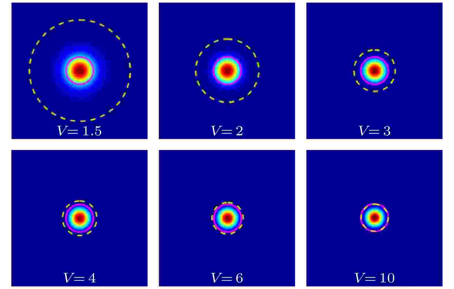
Abstract +
Owing to the advantages of high conversion efficiency, compactness and reliability, the fiber lasers are widely applied to many scientific areas, such as optical fiber communication, sensing and industrial processing. Beam quality is an important criterion for evaluating the performances of high-energy laser beam systems. Therefore, researchers have been constantly searching for the methods of evaluating the beam quality while pursuing higher output power. Until now, the researchers have proposed many definitions of beam quality. In practice, the evaluation parameters of beam quality include focused spot size, Strehl ratio, far-field divergence angle, diffraction limited β factor, energy circle rate, beam parameter product, and M 2 factor. Among them, the M 2 factor is the most suitable for the assessment of beam quality in both the near-field and far-field, which avoids the inaccuracy of the measurement of the beam quality only by the far-field radius or the far-field divergence angle. Thus, the M 2 factor is recognized as an important standard for evaluating beam quality by the International Organization for Standardization (ISO). However, it proves that the M 2 factor is not suitable for non-Gaussian distribution spot. On the other hand, in applications of high-energy laser beam transmission and laser industrial manufacturing, people pay more attention to the focusability of laser energy. In this case, the diffraction limited β factor is more suitable for evaluating beam quality. In this paper, we investigate the beam quality of LP01 mode of fiber laser by β factor, and a circular and solid homogenous beam with the energy of 99% of LP01 mode is considered as an ideal beam. The relationship between β factor and the parameters of LP01 mode in a step-index fiber is studied theoretically. It is found that the value of the beam quality β factor is lower than 1 when the normalized frequency V is bigger than 1.8, and the far-field energy focusability of LP01 mode is better than the case of ideal beam. Besides, the value of β factor decreases with the increase of normalized frequency V, core radius a or numerical aperture NA. In addition, the relationship between M 2 factor and β factor is non-linear.
EDITOR'S SUGGESTION
2021, 70 (20): 204204.
doi: 10.7498/aps.70.20210682
Abstract +
In recent years, the high-power single-frequency fiber lasers have developed rapidly, and they have been used in nonlinear frequency conversion and gravitational wave detection. The main factors limiting the output power of single-frequency fiber lasers are the nonlinear effect and transverse mode instability (TMI) effect. In general, large-core fibers can mitigate nonlinear effects while small-core fibers help to suppress the TMI effect. Owing to the core diameter varying in the longitudinal direction, tapered double clad fiber (T-DCF) is a promising solution to simultaneously suppress the nonlinearity and TMI effects. In the present study, we have fabricated a piece of 2.2-m-long Ytterbium-doped T-DCF. The core diameter and the cladding diameter of this fiber vary gradually from 30.3 μm to 49.3 μm and from 245 μm to 404 μm, respectively. Using this homemade fiber, we constructe an all-fiberized single-frequency master oscillator power amplifier system, which is pumped by laser diodes with a central wavelength of 976 nm. The seed of the system has a central wavelength of 1064 nm, and output power of 30 mW. The T-DCF is coiled on a piece of cooling plate, whose output end is cleaved at a 8° angle. The laser is output to free space and collimated by a free-space collimator. After the collimator, dichroic mirror is utilized to strip out the residual pump power for measuring power, spectrum, time-domain signal and beam quality. The output power increases linearly with the pumping power increasing. When the pumping power is 502 W, the output power reaches 400 W. And there is no stimulated Brillouin scattering (SBS) nor TMI under the power level. The corresponding slope efficiency is 81.7% while the M2 is measured to be 1.29, exhibiting the single-mode output characteristic of the system. When the output power is further increased to 418 W, the TMI effect is observed, which limits further the power scaling of the single-mode output. To the best of our knowledge, this is the highest output power of single-frequency fiber laser based on home-made gain fibers. The results indicate that T-DCFs can simultaneously suppress the nonlinearity and TMI, thus providing a useful reference for further power scaling of single-frequency fiber lasers. Higher output power is expected by optimizing the parameters of T-DCF and the structure of system.
2021, 70 (20): 204206.
doi: 10.7498/aps.70.20210433
Abstract +
High order harmonic generation (HHG) is an important phenomenon when atoms or molecules interact with an intense laser field. It can be used to generate ultrashort laser source, and can also be used to investigate the atomic and molecular dynamics and obtain the electric structure information of molecules. All these require to understand in depth the mechanism of HHG. There are complicated interference effects in HHG spectra of molecules due to multiple re-collision atomic centers in the molecule. In this paper, spectra of aligned O2 molecule in linearly polarized laser field is investigated by using the Lewenstein' s model. The dependence of the spectrum on the angle θ between the nuclear axis of the molecule and the laser polarization direction is obtained. It is shown that the maximum yield of HHG occurs at θ of 45°, which is in consistence with the experimental result. In addition, it is found that there exists a minimum value in the HHG spectrum for any given value of θ. The harmonic order corresponding to the minimum increases with θ increasing. It is found that the minimum comes from the coherent superposition of contributions from two channels. One channel refers to that the ionized electron from one atomic center, subjected to the electric field of the laser, moves back to its parent atomic center and there it combines with the molecule and emits harmonics; while the other channel is that the ionized electron generated from one atomic center move back to the other atomic center to complete the combination and emission of harmonics. The angle θ-dependent phase difference between contributions from these two channels is calculated and the harmonic order corresponding to the minimum value is obtained. Finally, the reason why the yield of HHG is low for the case of the molecular axis parallel to the laser polarization direction is different from that for the case of the molecular axis perpendicular to the polarization direction. For the parallel case, the contributions to HHG from the two channels are both small so that the amplitude of their coherent superposition is small. While for the perpendicular case, the individual contribution from each channel is not small but their destructive interference leads to small yield in harmonicspectrum.
2021, 70 (20): 204601.
doi: 10.7498/aps.70.20210726
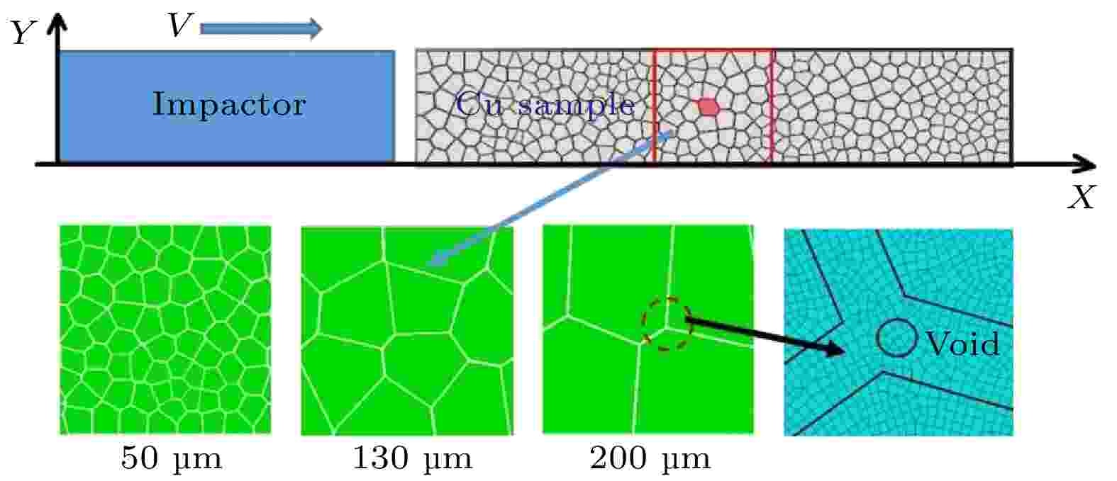
Abstract +
High-purity (HP) copper targets with grain sizes of 50, 130 and 200 μm are constructed by using the Voronoi method. Damage nucleation points are randomly prefabricated at the grain boundaries. A two-dimensional axisymmetric finite element model is established to simulate the spallation experiment of HP copper target. The effects of grain size and loading stress on the macro- mechanical response and meso-damage evolution of HP copper spallation are studied and compared with the relevant experimental results. Based on the analysis of free surface velocity profiles, the effects of grain size on the location of pull back velocity rebound point, velocity rebound slope and velocity rebound amplitude are revealed. It is demonstrated that the spalling strength corresponds to the peak value of tensile stress in the damage zone, which essentially represents the critical stress of micro damage nucleation or early growth. Based on the characteristic analysis of damage evolution nephogram, the evolution process of localized plastic strain field around the micro-voids in the growth and coalescence process is reproduced, and the strong dependence of micro-void coalescence behavior on grain size is clarified. The loading stress amplitude has little effect on the location of pull back velocity rebound point, but has a significant effect on the growth and coalescence behavior of micro-voids. The slope and amplitude of pull back velocity rebound increase with loading stress increasing, which is consistent with the relevant experimental result. With the increase of the loading stress, the micro-voids grow from independent growth to coalescence, thus forming spalling surface. The physical process of damage evolution determines the wave oscillation characteristics after the pull-back rebound point. The numerical simulation results reproduce the physical process of damage evolution and its influence on the macroscopic mechanical response, which is of great significance for further understanding spall damage evolution mechanism and theoretical model construction.
2021, 70 (20): 204602.
doi: 10.7498/aps.70.20210310
Abstract +
Defects that exist inside composites have an important effect on the tensile fracture properties of composites. The fiber bundle model is a theoretical model commonly used to study the tensile fracture properties of disorder materials. Existing work on fiber bundle models with single fiber defects shows that after single fiber defects are introduced into the fiber bundle model, the defects have a significant effect on the tensile fracture properties of the model. Since there are more complex microscopic defect structures in actual materials, such as voids, gaps, impurities, dislocations, micro-cracks, etc, it is necessary to build a multi-size defect model. In order to study the defects of different sizes and damage degrees existing in actual materials, the spatial size of the defect, the degree of defect and the distribution of fiber damage levels within the defect and other influencing factors are introduced to construct an extended fiber bundle model with cluster shaped defects. For the model, it is first assumed that the degree of defect of the fiber inside each cluster decays linearly from the center to the outside in two spatial attenuation forms: exponential decay and constant degree of defect. In the fiber bundle model of this cluster-shaped defect, the two most important factors are the number of defects α and the upper limit of defect size β. The numerical simulation method is used to analyze the influence of the number of defects, the upper limit of defect size, and spatial distribution of degree of defective fibers inside defect on the macroscopic mechanical properties and statistical properties of fracture when the model is subjected to quasi-static load borne under the nearest neighbor stress redistribution. Through the simulation analysis, it is found that owing to the overlapping competition mechanism of the defect spatial distribution, when the upper limit β of the defect size is large, the influence of the number of defects on the system load capacity trends to saturation. Since the defect degree of the defect center fiber is proportional to the defect size, with the upper limit β of the defect size increasing, its influence on the load capacity of the model becomes more and more significant. When large size defects exist, even if the number of defects is small, the load bearing performance of the material will be significantly reduced. The spatial distribution function of the damage degree of fiber inside the defect has no substantial influence on the above rules, and only changes the specific value of each fracture property. The simulation analysis results in this paper have certain theoretical significance in improving the mechanical properties of composite materials.
2021, 70 (20): 204701.
doi: 10.7498/aps.70.20210294
Abstract +
The evaporation process of drops on a solid surface is widely applied to daily life and industrial fields. Both contact angle hysteresis and the sensitivity of gas-liquid interfacial tension to temperature are important factors affecting the drop evaporation reflected in the contact line and contact angle. To investigate the internal mechanism, according to the lubrication theory and slip boundary conditions, we establish a mathematical model of the drop evaporation on a uniformly heated solid wall with considering the effect of contact angle hysteresis. This model is numerically solved by using a coordinate transformation method and Freefem++14.3, a highly efficient solver. The accuracy of the numerical calculation method is verified by comparing the numerical results with experimental results, and the grid independence is validated. The effect of contact angle hysteresis on the dynamics of evaporating drops is discussed, and the evaporation characteristics of drops with different tension sensitivities of the air-liquid interface to temperature are further investigated. The results show that the contact angle hysteresis has an apparent influence on the drop evaporation process which includes drop spreading stage, contact line pinning stage, and depinning stage. In the drop spreading stage, the increase in the hysteresis angle shortens the spreading time, and reduces the spreading velocity and radius, while in the contact line pinning stage, the pinning time is prolonged and the reduction of drop mass is significantly increased with hysteresis angle increasing. In the contact line depinning stage, the contact angle hysteresis reduces the contact angle, and a flatter shape emerges, thereby enhancing the ability to transfer heat and accelerating evaporation as well as shortening the depinning time. In addition, the large hysteresis angle leads to a large advancing contact angle and a small receding contact angle. The reduction in receding contact angle is more notable than the increment of advancing contact angle. The temperature sensitivity coefficient of the gas-liquid interfacial tension can be increased by reducing the receding contact angle, thereby improving the wettability of the drops on the wall enhancing the heat transfer and accelerating the evaporation. Regulating the contact angle hysteresis and the sensitivity of the interfacial tension to temperature can realize the manipulation of the drop movement, thus controlling the evaporation process.
PHYSICS OF GASES, PLASMAS, AND ELECTRIC DISCHARGES
2021, 70 (20): 205201.
doi: 10.7498/aps.70.20210737
Abstract +
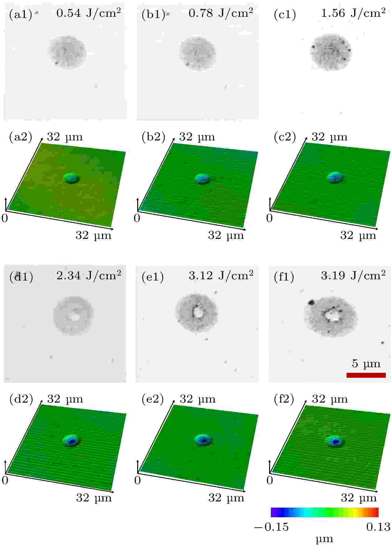
Femtosecond laser treatment has been widely used for modulating different kinds of materials as a convenient and efficient approach. In the process of laser modulation, the ionization caused by femtosecond laser irradiation may significantly affect the propagation and energy deposition of laser pulse inside the material, and thus finally influencing the surface morphology and optimizing the material properties. In this work, the ablation of WS2 is conducted in a wide range of laser fluence by single pulse. With the increase of injected energy, the expansion of craters goes through a process from rapid growth to stabilization both in the direction of diameter and in the depth direction. And a plasma model is proposed to track the dynamic response of the excited material and the transfer and deposition of the laser energy in the irradiation of WS2. The calculated results reveal that a great number of free electrons will generate after the incidence of laser pulse and leads the dense plasma zone to form. In this zone, the reflection on the surface and the absorption inside of WS2 are both enhanced due to the rapid increase of free electron density, which affects the injection and deposition of laser energy, thus resulting in the deposition of most energy in the shallow area below the surface. With the increasing of the laser fluence, the majority of laser energy is deposited on the surface of WS2, which leads the ablation crater to reach the saturation state. Meanwhile, a double-pulse train generated by temporal shaping is utilized to modulate the diameter of craters. By adjusting the pulse delay, the smallest diameter of the crater can be obtained at 0.7 ps. The results pave the way for potential applications of the effective method in controlling the material removal and improving the catalytic performance of pristine WS2.
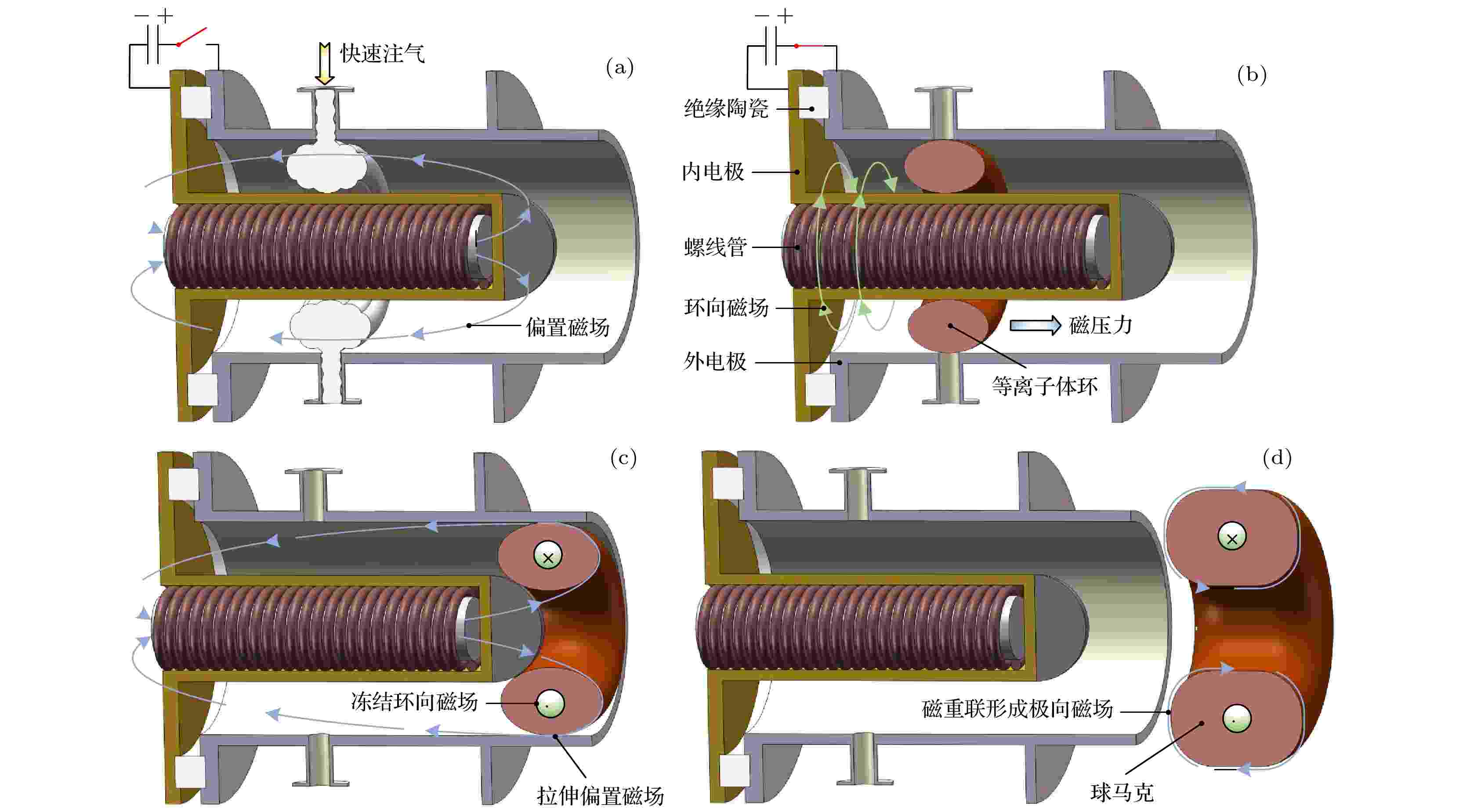
Effects of magnetized coaxial plasma gun operation on spheromak formation and plasma characteristics
2021, 70 (20): 205202.
doi: 10.7498/aps.70.20210709
Abstract +
Spheromak plasma formed by a magnetized coaxial plasma gun possesses high propagation velocity and electron density, which has been extensively investigated, for it has a variety of applications, such as fueling of fusion reactor, magnetized target fusion, and labratory simulations of astrophysical phenomena. Formation and optimization of the gun-type spheromak are studied by investigating the discharge characteristics of the gun and the scaling of plasma parameters with various operation conditions. Based on the spheromak formation mechanism, several significant operation parameters are identified, including peak value of gun current, bias flux, gas-puffed mass and the length of neutral gas distribution inside the gun channel: this length can be controlled by adjusting the time delay between gas injection and discharge of the capacitor bank to initiate gas breakdown and for a long time delay the current path distribution inside the gun channel can be characterized by a moving plasma ring which carries almost all of the gun current. Under a sufficient pressure of the self-generated field, the moving plasma ring with freezed toroidal field pushes the bias field into the vacuum chamber, the twisted field lines are then broken, reconnected, and thus forming a free spheromak. The injected gas is desired to exist only in the gun channel: if downstream region of the gun is filled with neutral gas, a weakly ionized and cold spheromak will be formed, which is not beneficial to practical applications. The multiple current path phenomenon is observed using two spatially separated magnetic coils inside the gun channel, excepting for the plasma ring, there are a stagnant current path and a reversed current path separately located in upstream and middle region of the gun channel. Development of the upstream current path is due to the residual charged particles deteached from the tail of accelerated plasma ring and the unswept netural particles, which reduces the energy injected into the plasma ring from capacitor bank, and thus having a negative effect on the performance of spheormak. The axial propagation velocity of spheromak, electron temperature and density are shown to increase with the capacitor bank voltage rising, which can be attributed to the elevation in energy injected into the plasma ring. Only higher electron density is obatined by increasing the gas-puffed mass, and the propagation velocity and electron temperature are observed to decrease. The energy injected into the plasma ring is independent of the gas-puffed mass, and electron density is elevated with gas-puffed mass increasing. Since the frequency of electron impact ionization increases, electrons undergo more collisions and transfer more energy to other particle species, thus the thermal energy of electrons decreases.
2021, 70 (20): 205203.
doi: 10.7498/aps.70.20210653
Abstract +
2021, 70 (20): 205204.
doi: 10.7498/aps.70.20210792
Abstract +
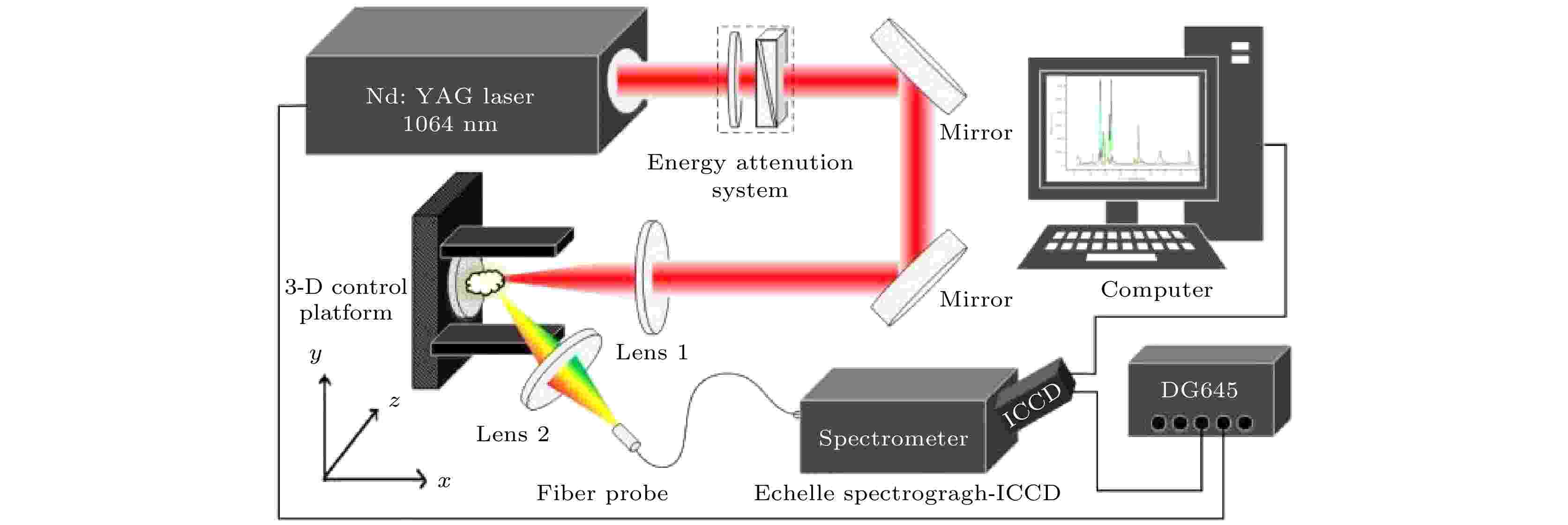
The concentration of Fe in aluminum alloy can affect the plasticity, heat resistance, strength and stress corrosion resistance of the alloy. The quantitative analysis of aluminum alloy composition is an important part of the online detection of alloy composition. To improve the quantitative analysis accuracy of Fe in aluminum alloy, the spatial confinement nanosecond laser-induced breakdown spectroscopy is combined with the gradient-descent method. By collecting laser-induced aluminum alloy plasma emission spectra, it is found that the plasma radiation intensity under the confinement of the plate space is significantly enhanced. The enhancement factor of the plasma emission spectrum with a plate spacing of 10 mm is 2.3. The internal standard method and the gradient descent method are used to establish the calibration models respectively, and the values of fitting coefficient (R2), root mean square error (RMSE) and average relative error (ARE) of the two models are compared. Without plate spatial confinement, the R2, RMSEC, RMSEP and ARE of the Fe element calculated by the internal standard method are 90.66%, 0.1903%, 0.1910% and 9.2220%, respectively. The R2, RMSEC, RMSEP and ARE of Fe element obtained by the gradient descent method are 97.12%, 0.1467% (weight concentration), 0.1124% (weight concentration) and 7.1373%, respectively. With the plate spatial confinement, the R2, RMSEC, RMSEP and ARE of Fe element calculated by the internal standard method are 95.22%, 0.1409% (weight concentration), 0.1401% (weight concentration), and 6.8893%, respectively. The R2, RMSEC, RMSEP and ARE of Fe element obtained by the gradient descent method are 99.22%, 0.0731% (weight concentration), 0.0756% (weight concentration) and 3.5521%, respectively. Comparing with the internal calibration model, the accuracy and stability of the gradient descent calibration model are improved. The spatial confinement LIBS combined with the gradient descent method can effectively reduce the influence of the alloy matrix effect and the self-absorption effect on the quantitative analysis.
2021, 70 (20): 205205.
doi: 10.7498/aps.70.20210484
Abstract +
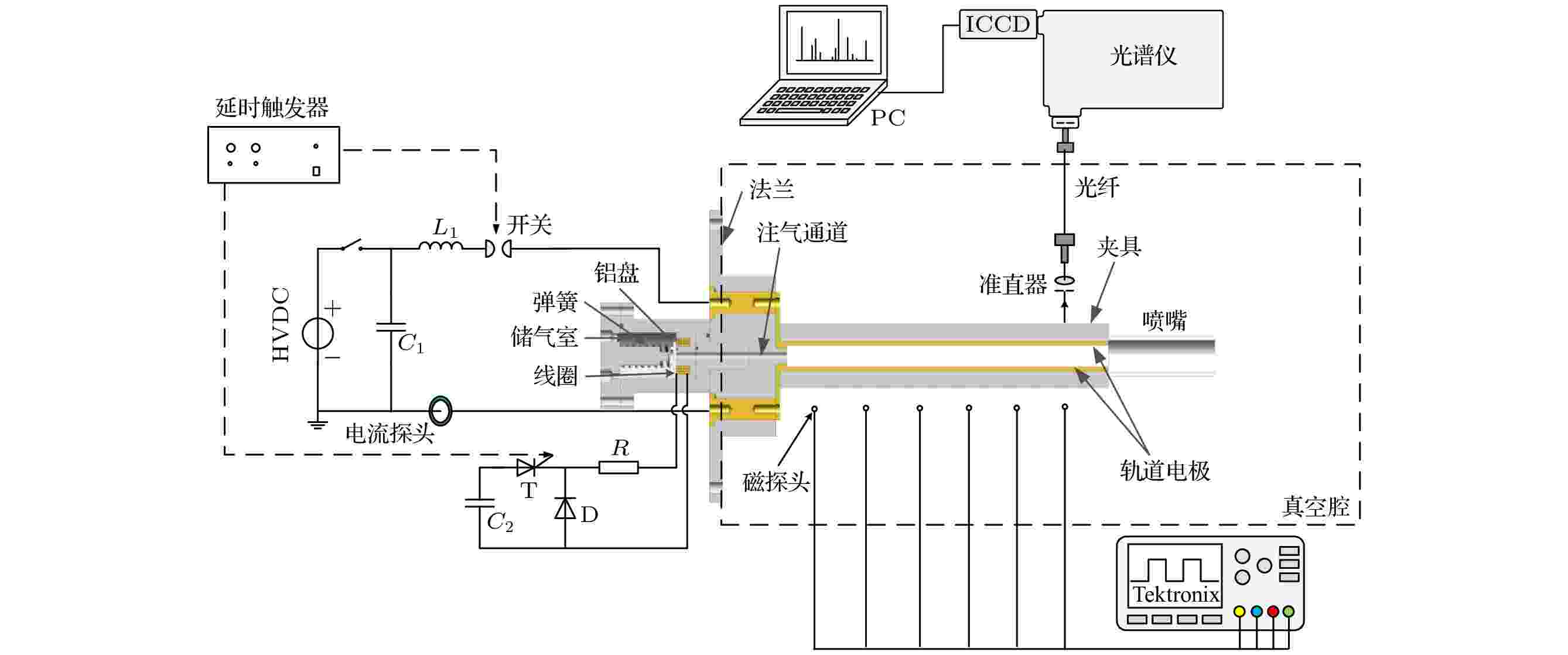
Electromagnetic plasma accelerators which can generate hypervelocity and high density plasma jets have been widely used in the fields of nuclear physics and astrophysics. In this paper, an experimental platform of parallel-rail accelerator electromagnetically driven plasma is established, and the discharge modes under different discharge currents and gas injection conditions are studied through using magnetic probes, a spectrometer and an ICCD. A fast gas valve is used to inject argon into the rail electrode area. The time delay between the fast valve discharge and the parallel-rail accelerator discharge is fixed to be 450 μs. The waveform of power supply of the parallel-rail accelerator is a sinusoidal wave. The total capacitance is 120 μF, the total inductance is about 400 nH, and the maximum current is 170 kA. The fast valve current waveform is a double exponential waveform with a maximum current of 2.5 kA. When the discharge current is 40 kA, a current sheet with a certain thickness is generated, and the current sheet moves through different detection positions along the rail electrode at a certain velocity. Therefore, the working mode of the parallel-rail accelerator is the snowplow mode. As the discharge current increases, the trailing edge of the current channel is fixed during the current rising phase, and starts to move to the end of the rail during the current falling phase. A diffuse distributed current channel is formed, and the parallel-rail accelerator operates in a deflagration mode. As the gas injection mass increases, the current channel front velocity decreases to form a more concentrated distributed current channel, and the discharge mode turns into the snowplow mode. The stationary current channel in the deflagration mode is maintained mainly by ablating the electrode. The operating parameters mainly affect the rail voltage, which in turn affects the discharge mode of the parallel-rail accelerator. The rail voltage increases when the discharge current or the current rate of change increases. If the rail gap behind the current channel cannot withstand the high rail voltage under large discharge current or large current rate of change, the breakdown occurs, which results in the deflagration mode discharge.

2021, 70 (20): 205206.
doi: 10.7498/aps.70.20210583
Abstract +
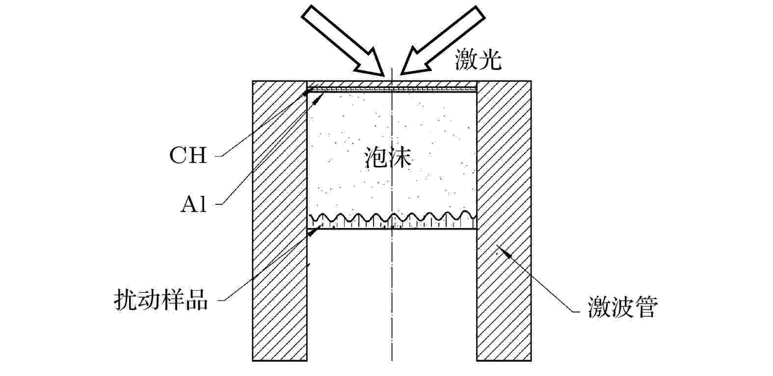
2021, 70 (20): 205207.
doi: 10.7498/aps.70.20210362
Abstract +
Micro-gap discharge is a form of gas discharge in which the discharge gap is on the order of sub-millimeters orless. To study the initial path of micro-gap discharge and the mechanism and law of particle density change during discharge, in this paper a micro-gap discharge experiment and discharge image acquisition device under atmospheric pressure is built and the COMSOL simulation software is used to simulate the electron density and space charge in the process of micro-gap air discharge. Furthermore, the MATLAB software is used to calculate the fractal dimension and probability development index of micro-gap discharge. The air discharge phenomena produced by applying positive DC voltage to needle tip at atmospheric pressure and room temperature with gap distance ranging from 50 μm to 150 μm are studied. It is found experimentally that there are twists and turns in the discharge channel, and the number of bifurcations in the discharge process with a short gap is less than that with a long gap. Observation of the micro-gap air discharge process with a gap of 100 μm under atmospheric pressure shows that the discharge process is divided into the following three processes: needle tip corona, corona breakdown streamer, and spark discharge channel. Based on the analyses of these experimental results, it can be concluded that the discharge mechanism follows Thomson's theory, supplemented by the streamer theory. The cathode secondary electron emission (including positive ions colliding with the cathode and photoelectron emission) and the space charge distortion electric field form a secondary electron avalanche to maintain the discharge together. The seed electrons formed by a small amount of space photoionization also form an electron avalanche under the action of the space charge distortion electric field. There are tortuous sections in the discharge channel, but the number of branches is small and the degree of tortuosity is low. Therefore, there are weak streamer forms. The discharge channel is tortuous and branched, but the number of bifurcations is relatively small, and the tortuousness is low. In addition, it is also found that a sheath is formed at the cathode, the distortion of electric field is 3–8 times that of original electric field, and the electron density reaches 2 × 10²¹ m–3 during discharge, obtained from the COMSOL simulation. Meanwhile, the fractal theory simulation is used to simulate the micro-gap discharge. In the process of research, the fractal dimension is found to be proportional to the voltage and the gap distance. When the probability development index η = 1.18–1.3, the fractal dimension of the simulated discharge process is closer to the experimental result. The findings in this paper lay the foundation for further exploring the discharge theory of sub-micro- and nano-scaled gaps.
CONDENSED MATTER: STRUCTURAL, MECHANICAL, AND THERMAL PROPERTIES
2021, 70 (20): 206801.
doi: 10.7498/aps.70.20210836
Abstract +
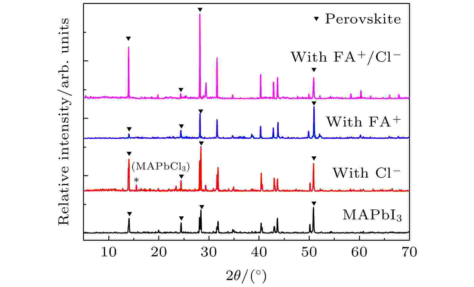
ABX3 crystalline perovskite material has many advantages: good photoelectric absorption property, high charge carrier mobility, good film formation, long charge carrier lifetime, and easy bandgap adjustment for absorption layer of perovskite solar cells. As a result, the power conversion efficiency (PCE) of the organic-inorganic halide perovskite solar cells (PSCs) has taken a tremendous step forward, from 3.9% in 2009 to a recently reported value over 25.5%. Thus, it shows great potential to compete with traditional silicon solar cells. However, PSCs preparing conditions are harsh and susceptible to environmental influences, thus leading to instability. Therefore, it is essential to prepare high-performance and stable PSCs in an air environment. This study aims to use the ion doping method to improve the performance and stability of PSCs and analyze the mechanism. This work focuses on enhancing PSCs efficiency and stability by performing FA+ and Cl– doping experiments on MAPbI3 films in air. The results show that a single Cl–-doping increases the carrier diffusion length, reducing the recombination of electrons and holes, and inducing the perovskite intermediate hydrate (CH3NH3)4PbI6·2H2O to form, promoting the crystallization of the thin film, and improving the device performance. On the other hand, a single FA+-doping will reduce the bandgap of perovskite and increase the short-circuit current density (JSC) of the device, and FA+ is susceptible to the influence of water vapor to induce a yellow δ-FAPbI3 perovskite film to form, which leads the device performance to degrade. However, the prepared co-doping Cl–, FA+ significantly improves overall PSCs device performance, yielding the highest PCE of 17.29%, and showing excellent stability by maintaining over 80% of the original PCE without any encapsulation after 1000-hour storage in ambient air.
2021, 70 (20): 206802.
doi: 10.7498/aps.70.20210892
Abstract +
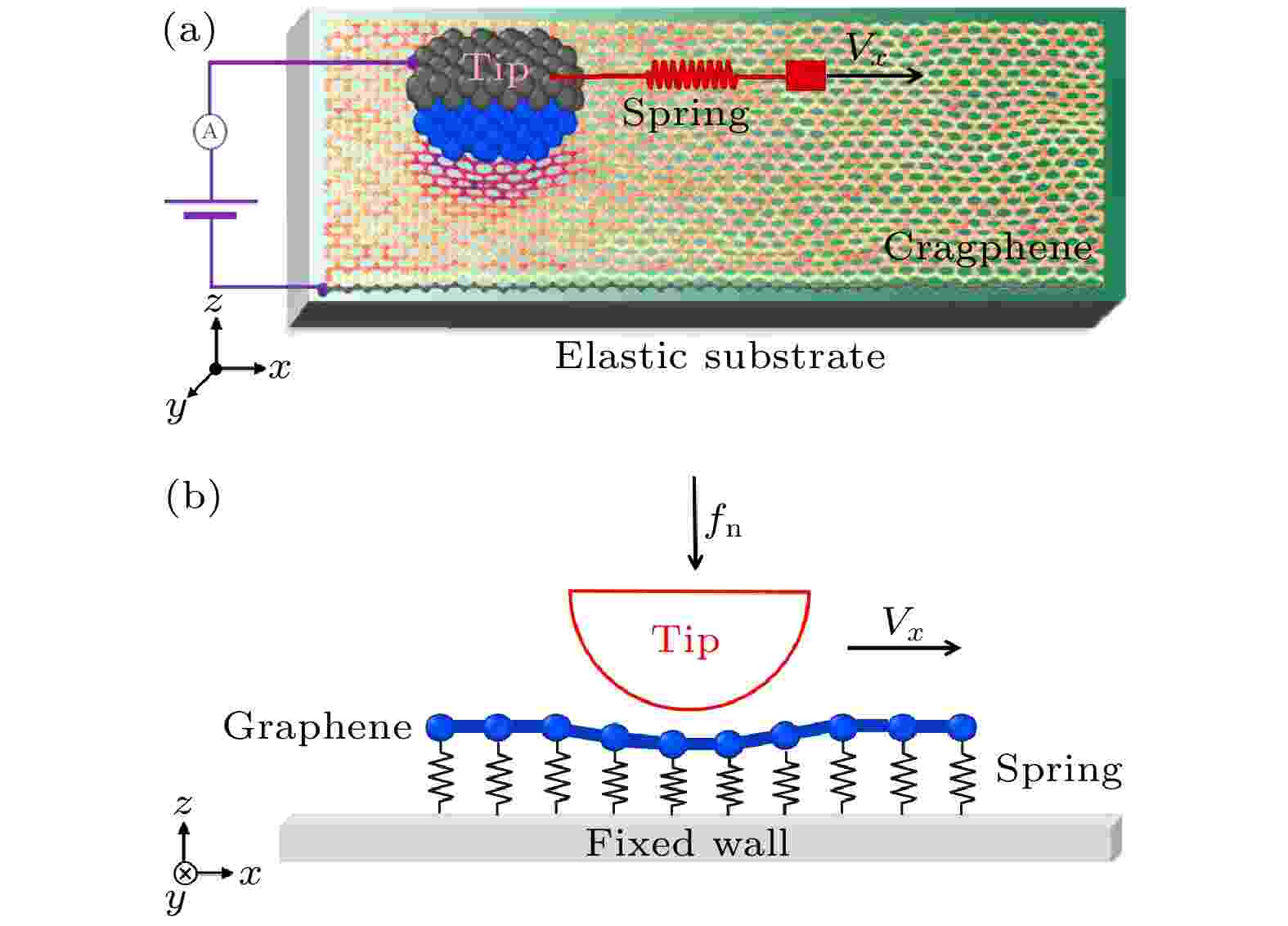
Graphene has shown the great potential applications in the field of solid lubricants due to its outstanding mechanical properties and chemical inertness. The introduction of interfacial current at the graphene-lubricated surface is expected to tune the lubrication performance of graphene. Here in this work, an atomistic configuration of single-crystal silicon tip sliding against graphene supported by an elastic substrate is constructed to investigate the current-carrying friction behavior of graphene by using molecular dynamics simulations. The effects of applied voltages, normal loads and substrate stiffnesses on the current-carrying friction behavior of graphene are systematically explored. The simulation results show that when the bias voltage is applied to the graphene-based system, the friction force undertaken by the tip is one order of magnitude larger than when applying no bias voltage. The friction increases with the magnitude of bias voltage increasing, but the increasing rate varies in different directions of bias voltage. A similar friction-voltage relationship of graphene under different normal loads and substrate stiffnesses indicates its relatively stable current-carrying friction behavior and the robust current-carrying effect. The increased friction force of graphene after the introduction of interfacial current can be attributed to the expansion of current-carrying region, causing Coulomb interactions instead of van der Waals interactions to dominate the adhesions at the friction interface. Based on the Prandtl-Tomlinson model, the current-carrying friction mechanism of graphene is systematically discussed. It is found that such a friction mechanism is different from the pucker effect of graphene, but follows the energy barrier theory. This work promotes the graphene to be used as the typical solid lubricant under the complex operation conditions with the voltage-induced current going through friction interfaces.
CONDENSED MATTER: ELECTRONIC STRUCTURE, ELECTRICAL, MAGNETIC, AND OPTICAL PROPERTIES
EDITOR'S SUGGESTION
2021, 70 (20): 207301.
doi: 10.7498/aps.70.20210949
Abstract +
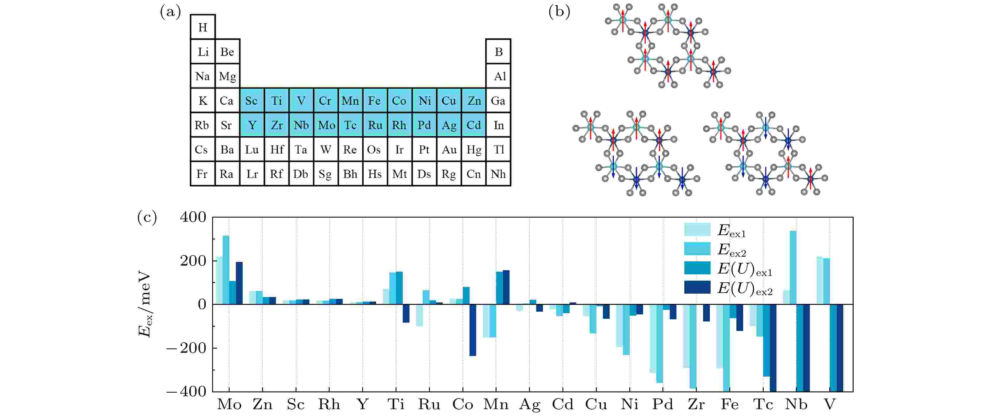
Two-dimensional magnetic semiconductors have received extensive attention due to their combination of magnetism, semi-conductivity and special two-dimensional structures, which also provide a new idea and platform for developing the nanometer spintronic and optoelectronic devices and also for conducting the related basic theoretical research. However, in addition to the common problems of two-dimensional magnetic semiconductor materials, such as volume manufacturing and environmental stability, the two-dimensional magnetic semiconductor materials have the unique difficulty, i.e. low Curie temperature, which makes it difficult to maintain ferromagnetic coupling at higher temperature. For example, the Curie temperature of the existing CrI3 monolayer is lower than 45 K, while that of the Cr2Ge2Te6 double-layer is only 20 K, which is far lower than the room temperature. Therefore, how to improve the Curie temperature of two-dimensional magnetic semiconductor materials through various approaches is one of the important issues that need to be resolved in this field of research. Based on the first-principles calculations, the exchange energies of a series of two-dimensional bimetallic iodides CrTMI6 (TM denotes transition metal elements in fourth and fifth rows) constructed from the lattice of CrI3 monolayer are preliminarily calculated and screened. Structures are fully relaxed until the force and the energy are converged to 0.01 eV/Å and 10–6 eV, respectively, and the ferromagnetic CrMoI6 monolayer is selected. Further calculations show that the band structure of the CrMoI6 monolayer exhibits ideal semiconductor characteristics with a band gap of about 1.7 eV. At the same time, theoretical calculations with considering the spin-orbit coupling show that the CrMoI6 monolayer has a considerable magnetic anisotropy (741.3 μeV/TM), and its easy axis is perpendicular to the two-dimensional plane. Monte Carlo simulation based on the Heisenberg model predicts that the Curie temperature of CrMoI6 monolayer reaches 92 K, which is about twice that of the CrI3 monolayer. The molecular dynamics and phonon spectrum calculations also prove that it has both thermal and kinetic stability. In addition, under the condition of applying compressive and tensile strain, its ferromagnetic coupling shows strong stability. This kind of magnetic transition metal halide which can be synthesized by alloying will further expand the family of two-dimensional magnetic materials and their applications in the field of spintronic devices.
2021, 70 (20): 207305.
doi: 10.7498/aps.70.20210145
Abstract +
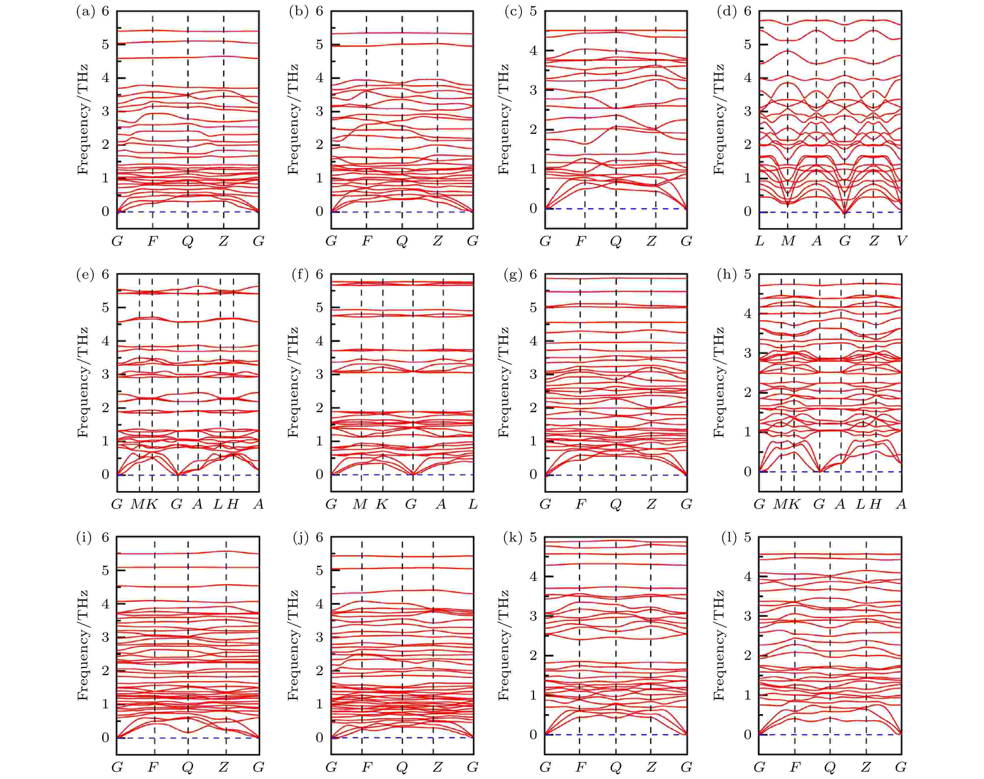
Ternary metal halides have attracted much attention as a new potential photoelectric material due to their ultra-high photoelectric conversion efficiencies. In this paper, USPEX, a crystal structure prediction software based on genetic algorithm, is used to investigate the potential crystal structures of ternary CuBiI compounds (CuBi2I7, Cu2BiI5, Cu2BiI7,Cu3BiI6, Cu3Bi2I9, CuBi3I10, and Cu4BiI7) at atmospheric pressure and absolute zero temperature. Based on the density functional theory, the formation energies, elastic coefficients, and phonon dispersion curves of the predicted structures are calculated. The twelve stable CuBiI compounds with good thermodynamic, dynamical and mechanical stabilities are identified. The twelve crystal structures of CuBiI compound feature mainly the co-existence of Cu—I and Bi—I bonds and coordination polyhedrons of I atoms. The band gaps of twelve structures, calculated by HSE06 method, are 1.13–3.09 eV, indicating that the stoichiometric ratio affects the band gap obviously. Among them, the band gaps of Cu2BiI5-P1, Cu2BiI7-P1 and Cu2BiI7-P1-II are relatively small, close to the optimal band gap value for light absorption (1.40 eV), demonstrating that these compounds are suitable for serving as light absorbing materials in solar cells. The distribution of density of state (DOS) indicates that the top of the valence band of CuBiI compound is attributed to the hybridized Cu-3d and I-5p orbitals; the bottom of the conduction band of Cu3BiI6-R3 comes mainly from the Bi-6p and I-5p orbitals, and Cu-3d contributes little; the conduction band bottom of Cu2BiI7 is mainly from the I-5p orbital, and the Cu-3d has little contribution. The bottoms of the conduction band of other structures originate mainly from the hybridized Bi-6p and I-5p orbitals. Electronic localization function and Bader charge analysis show that the Cu—I and Bi—I bonds have more ionic features and less covalent natures. The DOS distribution also confirms the covalent interaction of Cu/Bi-I. In addition, the CuBiI ternary compounds have extremely strong light absorption capacities (light absorption coefficient higher than 4 × 105 cm–1) in the high-energy region of visible light and high power conversion efficiency (31.63%), indicating that the CuBiI ternary compounds have the potential to be an excellent photoelectric absorption material. Our investigation suggests the further study and potential applications of CuBiI ternary compound as absorber materials in solar cell.
EDITOR'S SUGGESTION
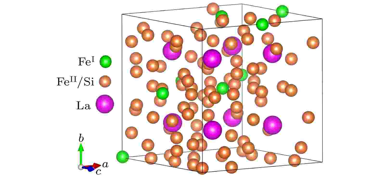
2021, 70 (20): 207501.
doi: 10.7498/aps.70.20211085
Abstract +
La(Fe, Si)13-based alloys have attracted more and more attention, for they exhibit giant magnetocaloric effects. In order to broaden their magnetic refrigeration temperatureranges, achieving a series of La(Fe, Si)13-based alloys with different magnetic phase transition temperatures is of great significance. Unlike the traditional research method, in this paper, a high-throughput first-principles computation is performed to estimate the magnetic phase transition temperature of the LaFe11.5Si1.5-based alloy by employing AMS-BAND software and the mean field theory. We investigate the effects of doping Mn, Co, Ni, Al atoms and Fe-vacancies on the magnetic phase transition temperature of LaFe11.5Si1.5-based alloy, and give the phase diagrams between the composition and magnetic phase transition temperature. The calculated results demonstrate that the magnetic phase transition temperature of the LaFe11.5Si1.5-based alloy increases with the increase of Co and Ni content. However, it shows an opposite result when Mn atom is doped. As for the LaFe11.5Si1.5-based alloy with the Fe-vacancies, the research results indicate that the absence of Fe atoms will reduce the magnetic phase transition temperature. Furthermore, when Mn, Co, Ni and Al atoms are doped in the alloys with Fe-vacancies, the variation tendency of the magnetic phase transition temperature with the change of the doping content is similar to that without the Fe-vacancies. Some estimated results are compared with the experimental or reported results, showing that they are in good agreement with each other. The PDOS and the magnetic moments of Fe atoms in the Mn, Co, Ni, Al-doped LaFe11.5Si1.5-based alloys are calculated, in which only the doping of Mn atoms can increase the magnetic moments of Fe atoms. Using the method of high-throughput first-principles calculation can effectively reduce the research cost and improve the working efficiency. In addition, it can provide technical support for the experimental selection of magnetocaloric materials with appropriate magnetic phase transition temperatures.
2021, 70 (20): 207502.
doi: 10.7498/aps.70.20210611
Abstract +
The spin neuron is an emerging artificial neural device which has many advantages such as ultra-low power consumption, strong nonlinearity, and high integration. Besides, it has ability to remember and calculate at the same time. So it is seen as a suitable and excellent candidate for the new generation of neural network. In this paper, a spin neuron driven by magnetic field and strain is proposed. The micromagnetic model of the device is realized by using the OOMMF micromagnetic simulation software, and the numerical model of the device is also established by using the LLG equation. More importantly, a three-layer neural network is composed of spin neurons constructed respectively using three materials (Terfenol-D, FeGa, Ni). It is used to study the activation functions and the ability to recognize the MNIST handwritten datasets.c Results show that the spin neuron can successfully achieve the random magnetization switching to simulate the activation behavior of the biological neuron. Moreover, the results show that if the ranges of the inputting magnetic fields are different, the three materials' neurons can all reach the saturation accuracy. It is expected to replace the traditional CMOS neuron. And the overall power consumption of intelligent computing can be further reduced by using appropriate materials. If we input the magnetic fields in the same range, the recognition speed of the spin neuron made of Ni is the slowest in the three materials. The results can establish a theoretical foundation for the design and the applications of the new artificial neural networks and the intelligent circuits.
2021, 70 (20): 207801.
doi: 10.7498/aps.70.20210602
Abstract +
The bimetallic nanoparticle can effectively integrate the physical and chemical properties of two metals and simultaneously exhibits the unique natures of each metal. It also serves as a good candidate for improving light scattering, photothermal conversion, plasmon resonance decay, and photon excitation. Investigating the optical properties of an individual nanoparticle can avoid the interaction between nanoparticles during experimental research, which allows us to more effectively analyze the interaction between the incident light and nanoparticles. In this work, the finite-difference time-domain method is used to study the spectral absorption characteristics of the plasmon bimetallic core-shell nanoparticles by calculating the spectroscopic properties, and also the distributions of the magnetic field, electric field, and absorption power during energy transmission and decaying. The results show that the resonance wavelength is red-shifted if the core diameter is increased. In addition, the absorption rate of Ag@Pt bimetallic nanoparticles is higher than that of pure Ag@Ag nanoparticles when the core diameter is bigger than 100 nm. This is because the strong shielding effect between the shell metal material and the core metal material leads the incident light to interact only with the outer atoms, resulting in resonance. Meanwhile, the plasmon of the Ag core decays faster than that of the Pt shell and more energies are transferred to the Pt shell. As a result, the surface of the Pt shell shows more concentrated magnetic and electric fields associated with an enlarged absorbing power. Moreover, the energy in the Ag core tends to transfer to the nearby Pt shell, which is characterized by the energy absorption in the Pt shell close to the Ag core, and is more concentrated. This paper provides theoretical guidance for designing plasmon bimetallic core-shell nanoparticles, thereby satisfying the demands for special spectral responses.

2021, 70 (20): 207802.
doi: 10.7498/aps.70.20210908
Abstract +
Owing to their excellent optical properties, perovskite quantum dots become ideal materials for conventional optoelectronic devices such as solar cells, light-emitting diodes, lasers, detectors, and non-classical quantum light sources such as single photon sources and entangled photon sources. The research on the photoluminescence blinking dynamics of single perovskite quantum dots can provide technical support for the preparation of nano-optoelectronic devices. In recent years, some achievements have been made based on the photoluminescence lifetime and photoluminescence intensity of single perovskite quantum dots. In this paper, the bright (on) state probability density and the dark (off) state probability density are extracted from photoluminescence intensity trajectories of single quantum dots and fitted by the (truncated) power-law function. It is found that the on-state probability density of single perovskite quantum dot under weak excitation condition can be fitted by a power-law function, which indicate that the photoluminescence blinking originates from the activation and deactivation of surface trap states. Under strong excitation condition, the on-state probability density of single perovskite quantum dot obeys exponential truncated power-law statistics, which indicate that the photoluminescence blinking is affected not only by the surface trap state, but also by the charging and discharging process.
2021, 70 (20): 207803.
doi: 10.7498/aps.70.20210500
Abstract +
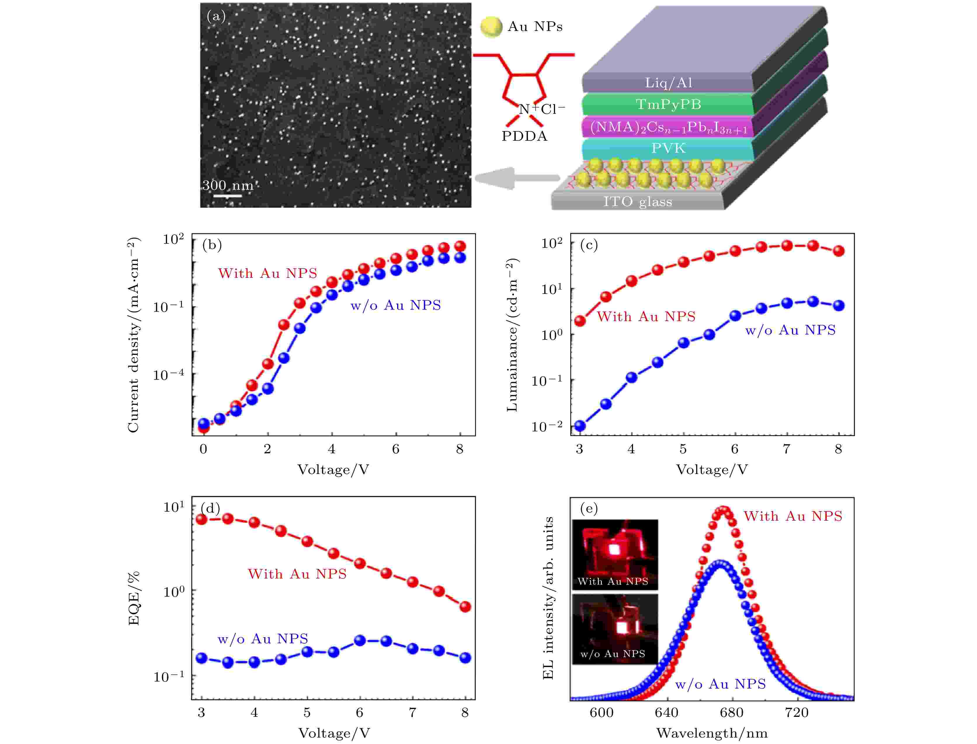
Gold nanoparticles (Au NPs) play an important role in improving the external quantum efficiency of perovskite light emitting diodes (PeLED). To avoid direct contact between the Au NPs and the light emitting layer, the Au NPs@SiO2 structure and blending the Au NPs into the hole transport layer (HTL) or electron transport layer (ETL) have been proposed previously. However, the Au NPs@SiO2 is difficult to obtain and affects the charge transport. When the Au NPs is blended in poly(3,4-ethylene dioxythiophene):poly(styrene sulfonate) (PEDOT: PSS), the density of Au NPs is not easily controlled and the PEDOT:PSS is not an ideal HTL for PeLED. Therefore, the electrostatic adsorption is used in this work to uniformly disperse the ~20 nm-size Au NPs on the top of the ITO anode, and the Poly(9-vinylcarbazole) (PVK) is spin-coated as the HTL to achieve the high performance red PeLED based on the (NMA)2Csn–1PbnI3n+1. After the Au NPs modification, the maximum luminous brightness rises from ~5.2 to ~83.2 cd/m2. Meanwhile, the maximum external quantum efficiency rises from ~0.255% to ~6.98%. Mechanism studies show that microcavity can be formed between the Au NPs-modified ITO anode and the Al cathode, and the transmitted light and the reflected light interfere with each other to improve the output couple efficiency of the PeLED. The photoluminescence (PL) spectrum and angle dependent PL intensity of the Au NPs-modified PeLED prove that the fluorescence enhancement of the (NMA)2Csn–1PbnI3n+1 perovskite is attributed mainly to the microcavity effect. Furthermore, the effects of Au NPs density on the performance of the PeLED are investigated, which reveals that the device with ~15 min adsorption is optimal. Finally, we rule out the contributions of Au NPs to the morphology, crystallization, electrical properties and localized surface plasmon resonance (LSPR) effects of (NMA)2Csn–1PbnI3n+1 perovskite films. In this work, the Au NPs are successfully applied to red PeLED for the first time, providing a feasible way of developing the low-cost and high-efficiency PeLED.
2021, 70 (20): 207804.
doi: 10.7498/aps.70.20210782
Abstract +
GaAs-based semiconductor doping technology, in which impurity energy levels are introduced into the band gap, can give rise to a decisive effect on its electrical and optical properties. When GaAs material is reduced to one-dimensional nanoscale, due to the increase of specific surface area, wurtzite- zinc blende coexisting structure is prone to appearing. GaAs nanowire doping can not only adjust its electro-optical properties, but also have a significant regulatory effect on its structural phase transition. The effects of beryllium (Be) and silicon (Si) doping on crystal structure and optical properties of gallium arsenide (GaAs) nanowires (NWs) are studied in this paper. Primitive, Si-doped and Be-doped GaAs NWs are grown on Si(111) substrates by molecular beam epitaxy in virtue of the self-catalyzed growth mechanism. The Raman spectra of primitive, Si-doped and Be-doped GaAs NWs are measured. The E2 mode peak unique to the WZ structure of primitive GaAs NWs is found in the Raman spectrum, and the E2 mode peak in the Raman spectrum of Si-doped GaAs NWs weakens or even disappears. Moreover, The E2 mode peak is not found in the Raman spectrum of Be-doped GaAs NWs. Furthermore, the structural changes of GaAs NWs are observed more intuitively by high-resolution transmission electron microscopy (HRTEM) and selected area electron diffraction (SAED). The PL spectra show that the wurtzite (WZ)-zinc blende (ZB) mixed phase II-type luminescence exists in primitive GaAs NWs, then the luminescence disappears due to Si or Be doping and turns into impurity defect related luminescence.
INTERDISCIPLINARY PHYSICS AND RELATED AREAS OF SCIENCE AND TECHNOLOGY
2021, 70 (20): 208201.
doi: 10.7498/aps.70.20210398
Abstract +
Lithium-rich manganese-based ternary cathode material for lithium-ion batteries, Li1.208Ni0.333Co0.042Mn0.417O2, has excellent structural stability and electrochemical stability due to its high Ni content. In order to understand the physical properties of this lithium-rich material, its crystal structure, electronic structure and defect properties are calculated by employing the first-principles method based on the density functional theory. The obtained electronic structure shows that Li1.208Ni0.333Co0.042Mn0.417O2 is a magnetic semiconductor with a direct band gap of 0.47 eV. The analysis of the electronic state suggests that the electronic state at the valence band maximum (VBM) is the hybridization of px, py, pz orbitals of oxygen and the dxy, dyz, dxz orbitals of Ni-atom. The electronic state at the conduction band minimum has similar characteristics to those at the VBM, however, part of Ni-${3{\rm{d}}}_{{x}^{2}-{y}^{2}}$ and Mn-${3{\rm{d}}}_{{x}^{2}-{y}^{2}}$ , and Mn-${3{\rm{d}}}_{yz}$ also contribute to the electronic hybridizations. The charge density difference calculations indicate that the bonding between O and transition metal atoms are through the mixture of covalent bond with ionic bond. The vacancy formation of a single metal atom is also calculated. The results show that the volumes of the defect systems containing metal vacancies are all reduced in comparison with the volume of perfect lattice. The volume change is the largest for the formation of Mn-vacancy, while the volume is almost unchanged with Co atoms extracted. The vacancy formation energies of the metals are Ef (Mn) > Ef (Co) > Ef (Ni), and the vacancy formation energy of Mn is significantly higher than those of Ni and Co, indicating that the presence of Mn provides a major structural stability for the material. The calculated charge density differences also show that the formation of metal vacancies influences only the charge distribution of the oxygen atoms around the vacancy, showing the local character of the vacancy effect. Since the formation of metal vacancy breaks the bonding between the metal and the surrounding oxygen atoms, the O-2p states near the Fermi surface are significantly increased as shown in the calculated electronic density of states. Such a picture suggests that the electrons on oxygen atoms in vicinity of the metal vacancies become freer.


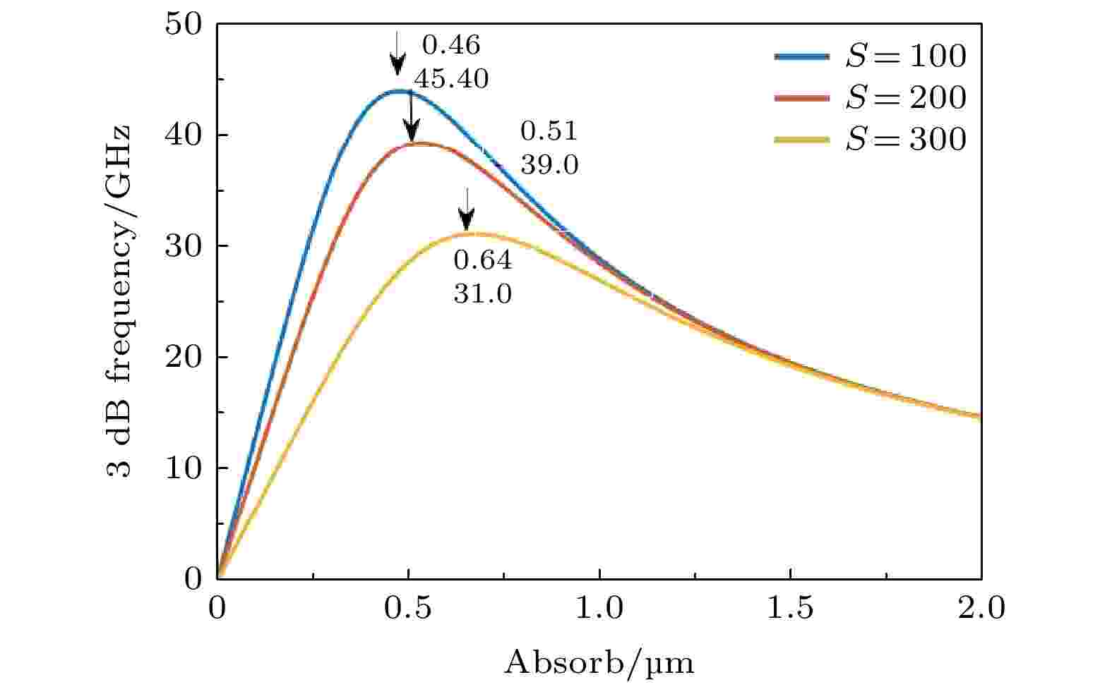
EDITOR'S SUGGESTION
2021, 70 (20): 208501.
doi: 10.7498/aps.70.20210781
Abstract +
Compared with surface and edge incident photodetectors, evanescent coupling photodetector (ECPD) has high bandwidth and high quantum efficiency, so it has a broad application prospect in the field of high-speed optical communication. The evanescent wave coupled photodetector is composed of a diluted waveguide, a single-mode ridge waveguide and a PIN photodiode. By directional evanescent wave coupling, the coupling efficiency of the incident light from the fiber to the absorption core of the photodetector is improved. In this paper, the structure design, experimental preparation and test results of an indium phosphorus based evanescent wave coupled photodetector array are introduced in detail. The test results show that the dark current of the evanescent wave coupled photodetector array is as low as 215 pA and 1.23 pA under –3 and 0 V bias, respectively. When the active area is 5 μm × 20 μm, the device still has a high responsivity of 0.5 A/W (without antireflection film). The high frequency performance of the detector is tested. The bandwidth of each detector is more than 25 GHz, and the total bandwidth is more than 400 GHz. Any optical device can be integrated. The detector array can be applied to the WDM receiving system of 400 Gbit/s and coherent receiving system of 200 Gbit/s.
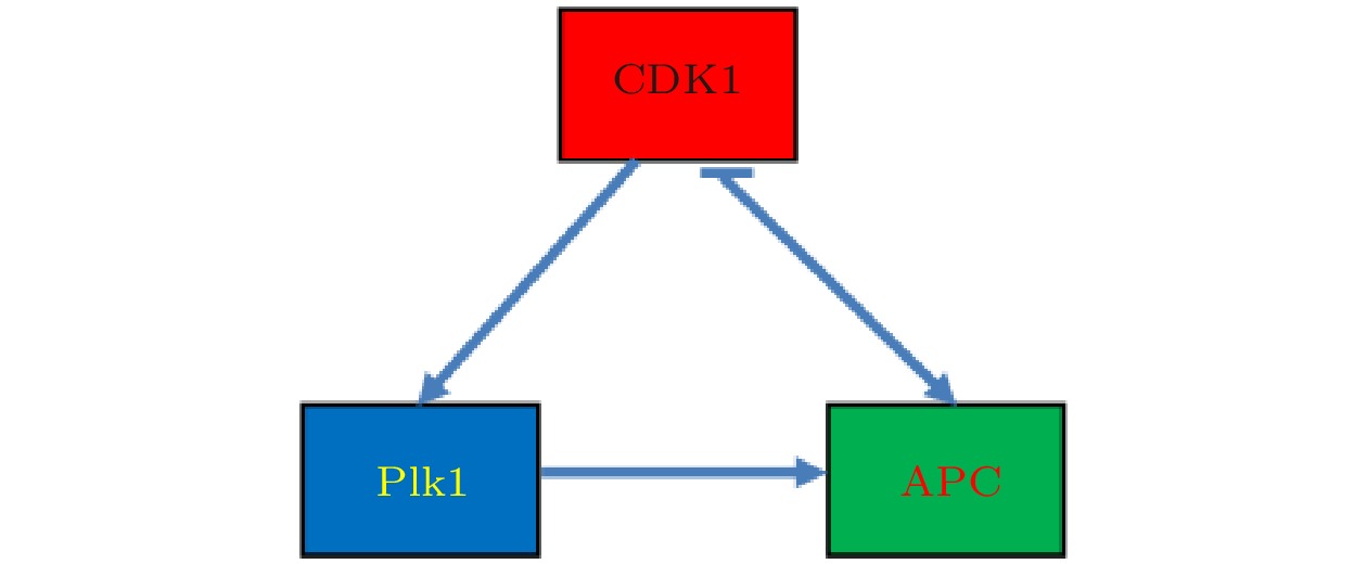
2021, 70 (20): 208701.
doi: 10.7498/aps.70.20210323
Abstract +
In this work, based on the Hill dynamics and Michaelis-Menten equation, a theoretical model is built to study the influence of time delay on the oscillation dynamics of a cyclin-dependent kinase 1 (CDK1)/ anaphase-promoting complex (APC) system. The theoretical model considers the time delay in the CDK1- polo-like protein kinase (P1K1)-APC pathway. We find that under different time delay conditions, the CDK1, Plk1 and APC exhibit periodic oscillation characteristics over time, indicating cell cycle progression. With the increase of time delay, the oscillation periods and amplitudes of CDK1, Plk1 and APC increase, which indicates that the time delay will change the dynamic characteristics of the system. It implies that during the cell cycle, the status of the CDK1/APC oscillation system will show a long-term correlation with the biochemical reaction time of each component, such as CDK1, Plk1 and APC. This correlation is influenced by its past, and there is a time-delay effect. The additional correction will be made due to time delay. By investigating the time-delay effect in Gaussian white noise environment, we find that in the Gaussian white noise environment, the noise disturbance obviously changes the dynamic characteristics of CDK1 evolution with time. In a low-noise environment, the CDK1/APC system changes the oscillation amplitude or period through self-adjusting time delay, so that the system can restore the stable periodic oscillation, while in a high noise environment, CDK1 exhibits a damped oscillation, indicating that the periodic oscillation dynamics of the CDK1/APC system will be significantly changed by strong noise. In the CDK1/APC system oscillation process, the system adjusts the physiological response through a feedback mechanism. There is a time delay between the perception of the noise effect and the establishment of an appropriate physiological response. By different time delays, the system can adjust complex non-periodic chaotic rhythms with different time delays, and recover to produce a stable periodic physiological process. Owing to the time delay, the CDK1/APC oscillation system changes from the original stable oscillation to a damped oscillation, but the original oscillation mode is difficult to recover. The theoretical results further reveal the time-delay effect in cell cycle processes such as Xenopus embryos, and provide a theoretical basis for designing pathway treatment plans that regulate cell cycle and block tumor transformation.

2021, 70 (20): 208801.
doi: 10.7498/aps.70.20210788
Abstract +
At present, there are many reports on the preparation of large area CH3NH3PbI3 perovskite solar cells based on ink-jet printing. These researches focus mainly on the ink-jet printing and electrode printing of perovskite active layer films. The hole transport layer, electron transport layer and other modified layers in the cell structure are still completed by spin coating or coating. In this work, we successfully realize large area CH3NH3PbI3 perovskite solar cells based on full ink-jet printing, including pen/Ag NWs bottom electrode, agnws top electrode, PEDOT: PSS hole transport layer, etc. It is found that the full inkjet printing can greatly reduce the material cost and simplify the production process, and obtain PC61BM layer, PEDOT: PSS layer, PEI layer and CH3NH3PbI3 perovskite thin film with high density and good uniformity. On this basis, we prepare the CH3NH3PbI3 perovskite solar cells with areas of 60, 80 and 100 cm2, respectively. The results show that when the concentration of perovskite ink is 1 mol/L, the printing speed is 30 mm/s and the substrate temperature is 50 ℃, the surface of perovskite film is smooth and the grain size is in a range of 500–600 nm. The surface roughness of the film is only 10 nm, so high-quality perovskite film can be obtained. The power conversion efficiency of the perovskite solar cell with an effective area of 60 cm2 is as high as 14.25% (VOC = 1.03 V, JSC = 19.21 mA/cm2, FF = 72%), which is the highest efficiency of perovskite solar cell prepared by full ink-jet printing method reported so far. In addition, when the device is placed in the air for 12 months without packaging, the photoelectric conversion efficiency is reduced to 80% of the initial value. However, the photoelectric conversion efficiency of FTPU package is reduced only by 5%, demonstrating good device stability.
