


-
ZnGeP2 crystals are the frequency conversion materials with the excellent comprehensive performances in a range of 3–5 μm. However, the overlap of the absorption band and the pump wavelength range of optical parametric oscillator at 8–12 μm limits the application performance of the optical parametric oscillator and makes it impossible to achieve a far-infrared laser output. In this work, the formation energy and migration mechanism of six kinds of defects of ZnGeP2 crystal are discussed by density functional theory. The results show that two defective structures of
$\rm{V_P}$ and$\rm{V_{Ge}}$ are difficult to form, while four defective structures of$\rm V_{\rm Zn}^ -$ ,$\rm{Z{n_{Ge}}}$ ,$ {\rm Ge}_{\rm Zn}^ + $ and$\rm{ G{e_{\rm Zn}} + {V_{\rm Zn}}}$ are easy to create. When the number of Ge atoms are slightly more than that of Zn atoms in ZnGeP2 crystals, the vacancy defects$\rm V_{\rm Zn}^ -$ form more easily than antistructure defects$ {\rm Ge}_{\rm Zn}^ + $ at 10 K, 500 K and 600 K, but the antistructure defects$ {\rm Ge}_{\rm Zn}^ + $ are easier to form than the vacancy defects$ {\text{V}}_{\text{Zn}}^{-} $ at 273 K and 400 K. There is a negative correlation between the volume expansion rate and the defect formation energy of ZnGeP2 crystal. The larger the volume expansion rate, the lower the defect formation energy is. The differential charge density shows that the electron cloud density among the atoms is enhanced in the defective structures of GeZn and VZn+GeZn. The electron cloud density at the lattices of vacancy defects is enhanced when the vacancy defects (VZn and VGe) and antistructure defects (GeZn and ZnGe) form the joint defects. Comparing with the defect-free cells, the charge of Zn atoms increases significantly, that of Ge is significantly reduced, and that of P does not change in the antistructure defect ZnGe or GeZn. The absorption spectra of ZnGeP2 crystal at 10K show that there is the significant absorption in a wavelength range from 0.6 μm to 2.5 μm for the four defective structures: VGe, VZn, ZnGe and GeZn, while the absorption in this range is small for the defective structures VP and GeZn+VZn. The VZn has the lowest migration energy, while VGe has the highest. The difficulty for VP to migrate depends on the space resistance, while the difficulty for VGe and VZn to migrate depend on the inter-atomic distance. This may be related to the small radius and high proportion of P atoms and the large radius and low proportion of Ge and Zn atom in ZnGeP2 crystal.-
Keywords:
- defect structure /
- optical properties /
- ZnGeP2 /
- mid and far-infrared crystals
[1] Kolesnikov A V, Vasilenko A P, Trukhanov E M, Lei Z T, Zhu C Q, Yang C H, Verozubova G A 2022 J. Cryst. Growth 580 126479
 Google Scholar
[2] Cao Z H, Yang H, Sun S L, Liu Y H, Zhang M, Dai X J 2020 Opt. Mater. 110 110383
Google Scholar
[3] Lei Z T, Kolesnikov A, Vasilenko A, Zhu C Q, Verozubova G, Yang C H 2018 J. Appl. Cryst. 51 1043
Google Scholar
[4] Zinoviev M, Yudin N, Gribenyukov A, Podzyvalov S, Dyomin V, Polovtsev I, Suslyaev V, Zhuravlyova Y 2021 Opt. Mater. 111 110662
Google Scholar
[5] Shimony Y, Raz O, Kimmel G, Dariel M P 1999 Opt. Mater. 13 101
Google Scholar
[6] Rakowsky M H, Kuhn W K, Lauderdale W J, Halliburton L E, Edwards G J, Scripsick M P, Schunemann P G, Pollak T M, Ohmer M C, Hopkins F K 1994 Appl. Phys. Lett. 64 1615
Google Scholar
[7] Halliburton L E, Edwards G J, Scripsick M P, Rakowsky M H, Schunemann P G, Pollak T M 1995 Appl. Phys. Lett. 66 2670
Google Scholar
[8] Gehlhoff W, Azamat D, Hoffmann A 2003 Phys. Status Solidi B 235 151
Google Scholar
[9] Giles N C, Halliburton L E, Schunemann P G, Pollak T M 1995 Appl. Phys. Lett. 66 1758
Google Scholar
[10] Setzler S D, Giles N C, Halliburton L E, Schunmann P G, Pollak T M 1999 Appl. Phys. Lett. 74 1218
Google Scholar
[11] Gehlhoff W, Pereira R N, Azamat D, Hoffmann A, Dietz N 2001 Physica B 310 1015
[12] Gehlhoff W, Azamat D, Hoffmann A, Dietz N 2003 J. Phys. Chem. Solids 64 1923
Google Scholar
[13] Jiang X S, Miao M S, Lambrecht W R L 2005 Phys. Rev. B 71 205212
[14] Jiang X S, Miao M S, Lambrecht W R L 2006 Phys. Rev. B 73 193203
[15] Jiang X S, Lambrecht W R L 2009 Solid State Commun. 149 685
[16] Perdew J P, Burke K, Ernzerhof M 1996 Phys. Rev. Lett. 77 3865
Google Scholar
[17] Vanderbilt D 1990 Phys. Rev. B 41 7892
Google Scholar
[18] Laasonen K, Pasquarello A, Car R, Lee C, Vanderbilt D 1993 Phys. Rev. B 47 10142
Google Scholar
[19] Yan Y F, Wei S H 2008 Phys. Stat. Sol. B 245 641
[20] Wang C, Sun J, Gou H Y, Wang S P, Zhang J, Tao X T 2017 Phys. Chem. Chem. Phys. 19 9558
Google Scholar
[21] Setzler S D, Schunemann P G, Pollak T M, Ohmer M C, Goldstein J T, Hopkins F K, Stevens K T, Halliburton L E, Giles N C 1999 J. Appl. Phys 86 6677
Google Scholar
[22] Giles N C, Bai L H, Chirila M M, Garces N Y, Stevens K T, Schunemann P G, Setzler S D, Pollak T M 2003 J. Appl. Phys 93 8975
Google Scholar
-
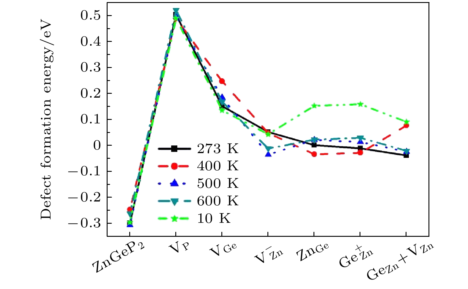
图 1 缺陷形成能与温度的关系曲线
Figure 1. Dependent curves of defect formation energy and temperature.
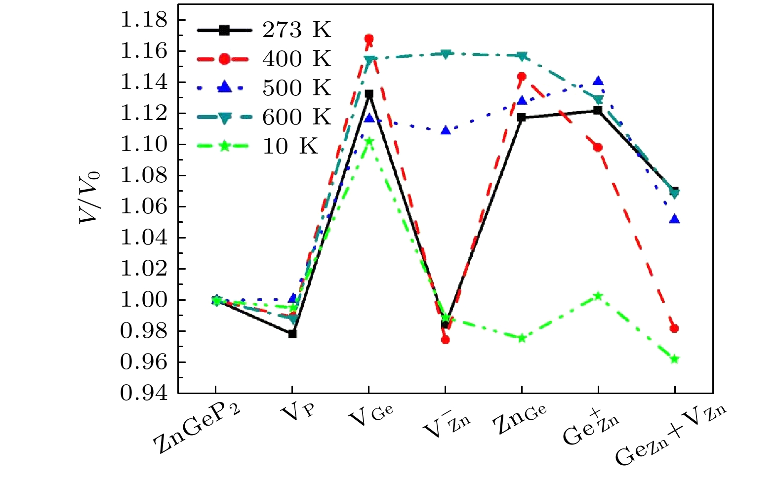
图 2 ZnGeP2缺陷晶胞体积变化率
Figure 2. Volume change rates of defective cells for ZnGeP2.

图 3 ZnGeP2晶胞 (a) 273 K完美晶胞; (b) 273 K时VP晶胞; (c) 500 K完美晶胞; (d) 500 K时VP晶胞
Figure 3. Unit cells of ZnGeP2 (a) Perfect cell at 273 K; (b) cell containing VP at 273 K; (c) perfect cell at 500 K; (d) cell containing VP at 500 K.
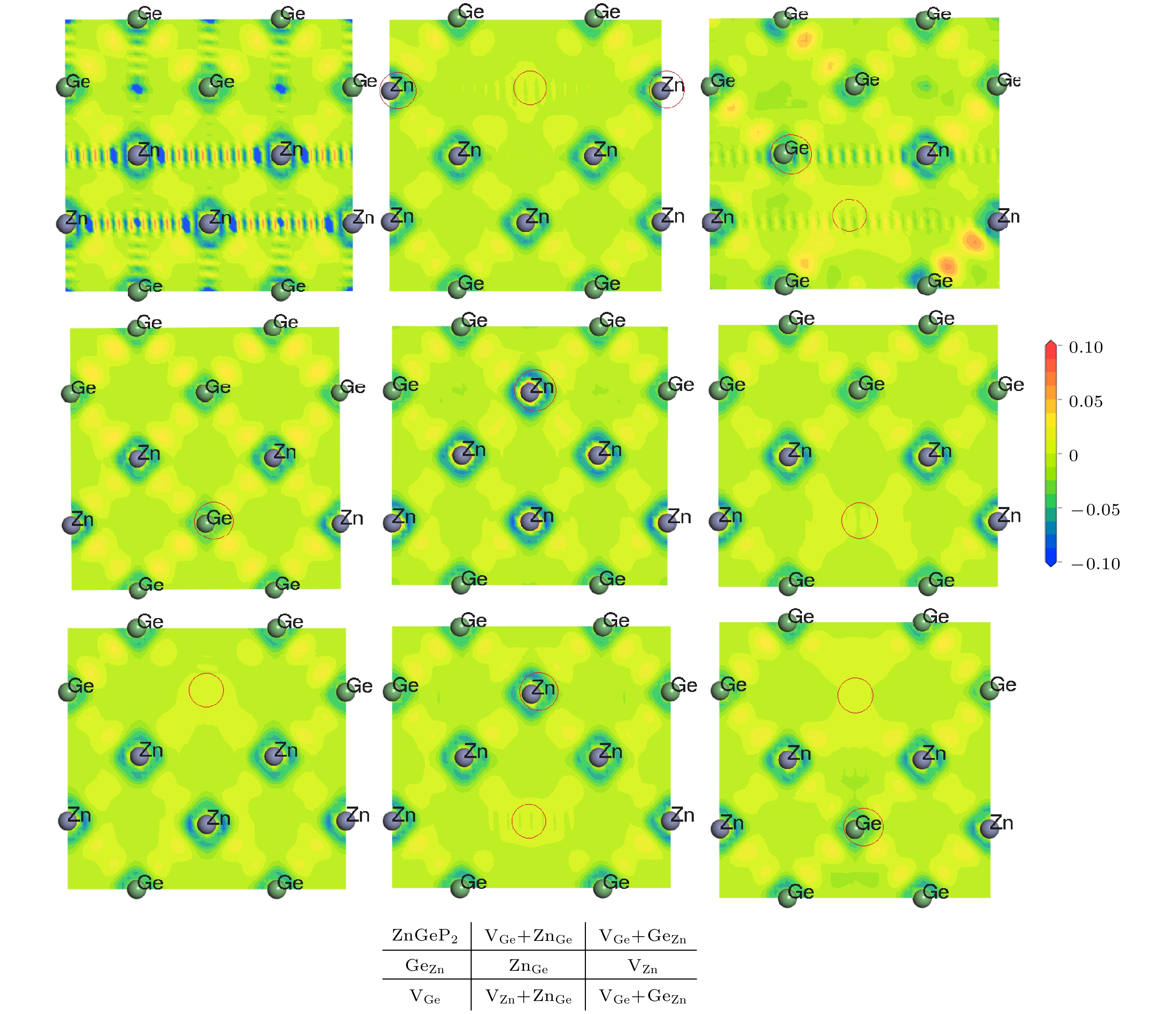
图 4 无缺陷晶胞和含缺陷晶胞(200)晶面的差分电荷密度分布图(红色圆圈为缺陷位置)
Figure 4. Differential charge density distribution of perfect cells and defective cells for (200) plane (red circles are defect positions) .

图 5 ZnGeP2缺陷晶胞的吸收谱
Figure 5. Absorption spectra of defective cells for ZnGeP2.
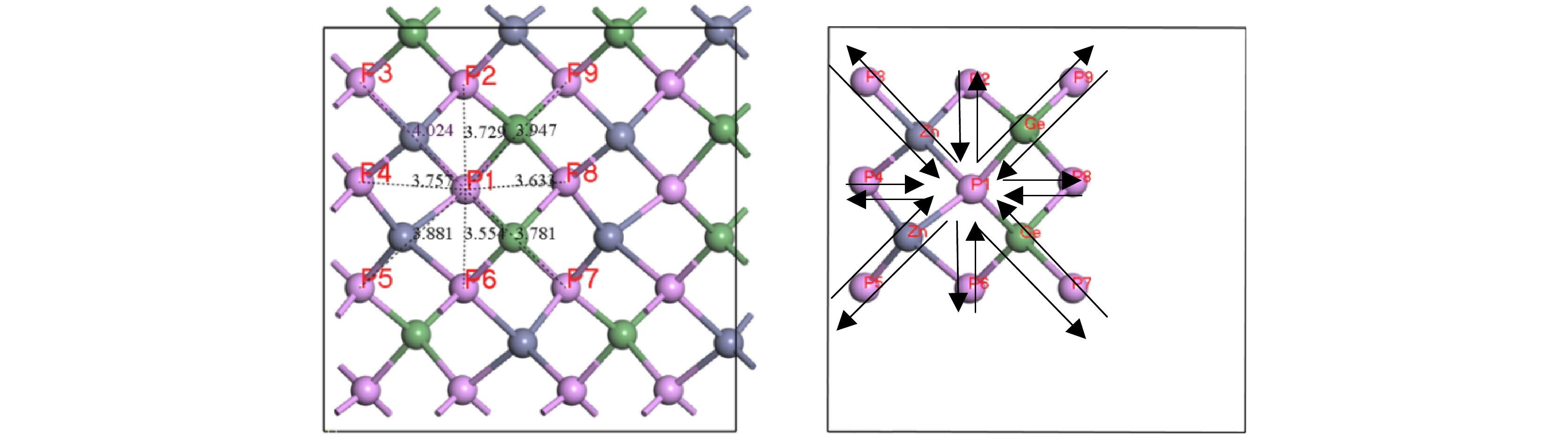
图 6 (010)面P原子标记图(采用2 × 1 × 1超胞体系)
Figure 6. Map of positions of P atoms for (010) plane (super cells of 2 × 1 × 1 are used).

图 7 (010)面P1格点空位向P4, P6, P8迁移的过渡态 (a) P1-P4; (b) P1-P6; (c) P1-P8
Figure 7. Transition states for migrations from P1 vacancy lattice to P4, P6 and P8 lattices for (010) plane: (a) P1-P4; (b) P1-P6; (c) P1-P8.

图 8 (100)面Ge原子标记图
Figure 8. Map of positions of Ge atoms for (100) plane.
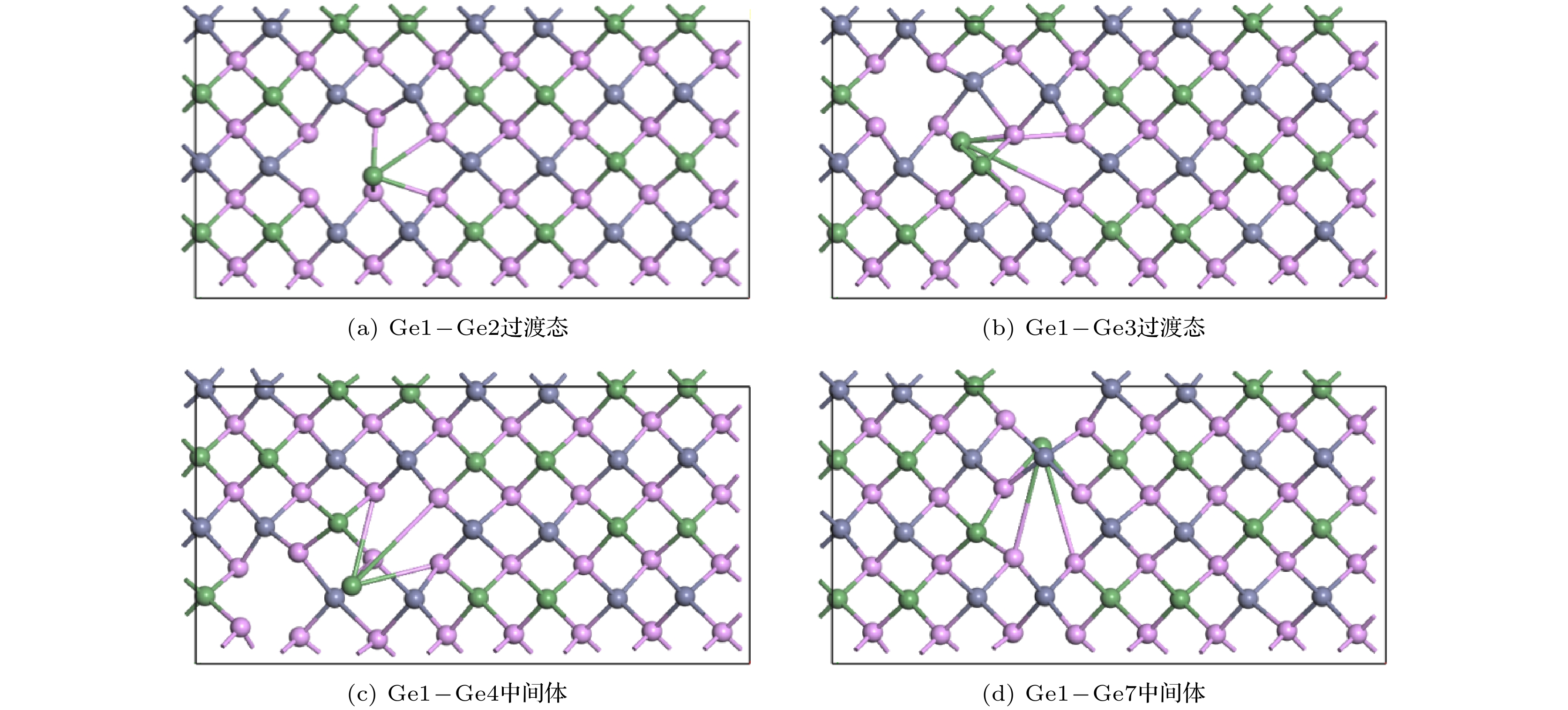
图 9 (100)面Ge1格点空位向Ge2, Ge3, Ge4, Ge7迁移的过渡态和中间体 (a) Ge1-Ge2过渡态; (b) Ge1-Ge3过渡态; (c) Ge1-Ge4中间体; (d) Ge1-Ge7中间体
Figure 9. Transition states and intermediate products for migrations from Ge1 vacancy lattice to Ge2, Ge3, Ge4 and Ge7 lattices for (100) plane: (a) Transition state of Ge1-Ge2; (b) transition state of Ge1-Ge3; (c) intermediate product of Ge1-Ge4; (d) intermediate product of Ge1-Ge7.
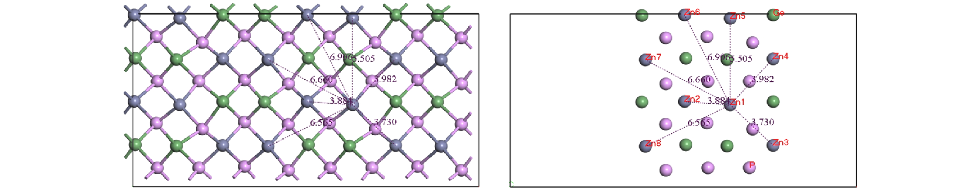
图 10 (100)面Zn原子标记图
Figure 10. Map of positions of Zn atoms for (100) plane.
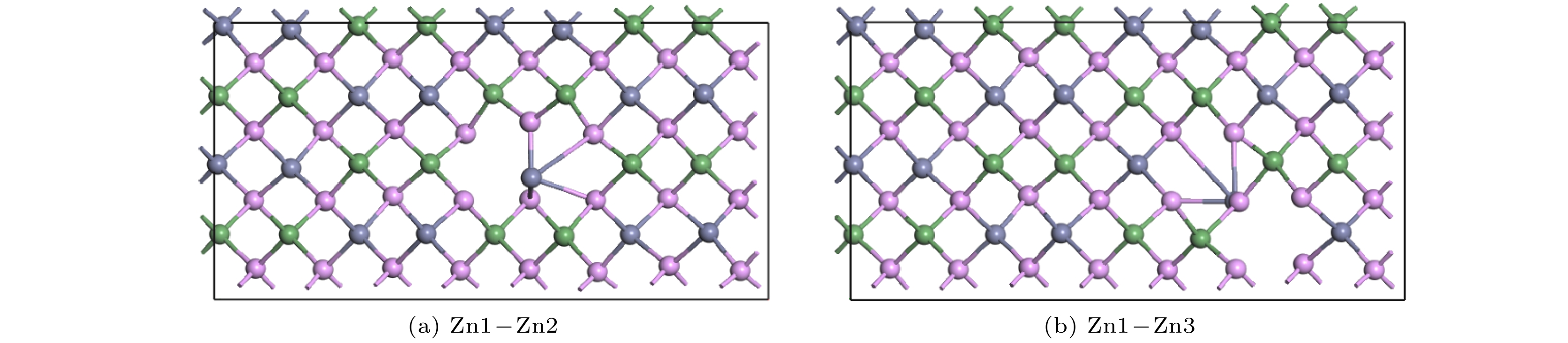
图 11 (100)面Zn1格点空位向Zn2和Zn3迁移的过渡态 (a) Zn1-Zn2; (b) Zn1-Zn3
Figure 11. Transition states for migrations from Zn1 vacancy lattice to Zn2 and Zn3 lattices for (100) plane: (a) Zn1- Zn2; (b) Zn1- Zn3
表 1 含
$ {\text{Z}}{{\text{n}}_{{\text{Ge}}}} $ 和$ {\text{G}}{{\text{e}}_{{\text{Zn}}}} $ 的缺陷晶胞替换元素电荷和对应的键长Table 1. Charge of substitution element and corresponding bond length of defective cells containing
$ {\text{Z}}{{\text{n}}_{{\text{Ge}}}} $ and$ {\text{G}}{{\text{e}}_{{\text{Zn}}}} $ .温度/K 元素 电荷 化学键 键长/nm 元素 电荷 元素 电荷 化学键 键长/nm 元素 电荷 273 无缺陷晶体 Ge4 0.69 Ge4-P6 2.35899 P6 –0.32 ZnGe Zn9 0.13 Zn9-P8 2.48614 P8 –0.34 Ge4-P4 2.35999 P4 –0.36 Zn9-P6 2.50023 P6 –0.4 Ge4-P8 2.34575 P8 –0.32 Zn9-P12 2.49713 P12 –0.38 Ge4-P3 2.28732 P3 –0.35 Zn9-P11 2.42738 P11 –0.33 Zn3 0.01 Zn3-P4 2.31271 P4 –0.36 GeZn Ge1 0.37 Ge1-P6 2.69564 P6 –0.36 Zn3-P3 2.34784 P3 –0.35 Ge1-P3 2.62636 P3 –0.32 Zn3-P6 2.40425 P6 –0.32 Ge1-P8 2.57614 P8 –0.32 Zn3-P8 2.46926 P8 –0.32 Ge1-P4 2.51162 P4 –0.35 600 无缺陷晶体 Ge4 0.68 Ge4-P6 2.23412 P6 –0.37 ZnGe Zn5 0.15 Zn5-P8 2.3525 P8 –0.37 Ge4-P4 2.34218 P4 –0.32 Zn5-P6 2.65332 P6 –0.32 Ge4-P8 2.40672 P8 –0.34 Zn5-P12 2.6305 P12 –0.34 Ge4-P3 2.34169 P3 –0.31 Zn5-P11 2.54137 P11 –0.36 Zn2 0 Zn2-P5 2.48759 P5 –0.33 GeZn Ge1 0.37 Ge1-P7 2.57682 P7 –0.33 Zn2-P7 2.37797 P7 –0.37 Ge1-P5 2.65679 P5 –0.34 Zn2-P3 2.3425 P3 –0.31 Ge1-P8 2.56753 P8 –0.33 Zn2-P8 2.40251 P8 –0.34 Ge1-P3 2.49967 P3 –0.29  DownLoad: CSV
表 2 (010)面P原子间距与迁移能
Table 2. P atomic spacing and migration energy for (010) plane.
原子间距/(10–10 m) 迁移能/eV 原子间距/(10–10 m) 迁移能
/eV原子间距/(10–10 m) 迁移能
/eVP1-P2 3.729 2.48595 P1-P3 4.024 2.54995 P1-P4 3.757 3.31980 P2-P1 3.729 2.45433 P3-P1 4.024 2.74953 P4-P1 3.757 3.24897 P1-P5 3.881 2.75197 P1-P6 3.554 2.28346 P1-P7 3.781 2.35649 P5-P1 3.881 2.67016 P6-P1 3.554 2.66777 P7-P1 3.781 2.27400 P1-P8 3.633 2.08976 P1-P9 3.947 2.68005 P8-P1 3.633 2.01885 P9-P1 3.947 2.87954
DownLoad: CSV
表 3 (100)面Ge原子间距与迁移能
Table 3. Ge atomic spacing and migration energy for (100) plane.
原子间距/(10–10 m) 迁移能
/eV原子间距/(10–10 m) 迁移能/eV 原子间距/(10–10 m) 迁移能
/eVGe1-Ge2 3.668 2.41507 Ge1-Ge3 6.682 4.84944 Ge1-Ge4 6.720 5.76056 Ge2-Ge1 3.668 2.16555 Ge3-Ge1 6.682 4.77747 Ge4-Ge1 6.720 5.68664 Ge1-Ge5 3.857 2.85194 Ge1-Ge6 3.906 2.67506 Ge1-Ge7 5.505 5.15750 Ge5-Ge1 3.857 2.80361 Ge6-Ge1 3.906 2.62691 Ge7-Ge1 5.505 5.15696 Ge1-Ge8 6.635 4.50346 Ge8-Ge1 6.635 4.21664
DownLoad: CSV
表 4 (100)面Zn原子间距与迁移能
Table 4. Zn atomic spacing and migration energy for (100) plane.
原子间距/(10–10 m) 迁移能
/eV原子间距/(10–10 m) 迁移能
/eV原子间距/(10–10 m) 迁移能
/eVZn1-Zn2 3.884 1.75494 Zn1-Zn3 3.730 2.03159 Zn1-Zn4 3.982 2.00985 Zn2-Zn1 3.884 1.81019 Zn3-Zn1 3.730 2.05914 Zn4-Zn1 3.982 2.04534 Zn1-Zn5 5.505 3.52642 Zn1-Zn6 6.906 5.04726 Zn5-Zn1 5.505 3.52635 Zn6-Zn1 6.906 5.12510
DownLoad: CSV
-
[1] Kolesnikov A V, Vasilenko A P, Trukhanov E M, Lei Z T, Zhu C Q, Yang C H, Verozubova G A 2022 J. Cryst. Growth 580 126479
Google Scholar
[2] Cao Z H, Yang H, Sun S L, Liu Y H, Zhang M, Dai X J 2020 Opt. Mater. 110 110383
Google Scholar
[3] Lei Z T, Kolesnikov A, Vasilenko A, Zhu C Q, Verozubova G, Yang C H 2018 J. Appl. Cryst. 51 1043
Google Scholar
[4] Zinoviev M, Yudin N, Gribenyukov A, Podzyvalov S, Dyomin V, Polovtsev I, Suslyaev V, Zhuravlyova Y 2021 Opt. Mater. 111 110662
Google Scholar
[5] Shimony Y, Raz O, Kimmel G, Dariel M P 1999 Opt. Mater. 13 101
Google Scholar
[6] Rakowsky M H, Kuhn W K, Lauderdale W J, Halliburton L E, Edwards G J, Scripsick M P, Schunemann P G, Pollak T M, Ohmer M C, Hopkins F K 1994 Appl. Phys. Lett. 64 1615
Google Scholar
[7] Halliburton L E, Edwards G J, Scripsick M P, Rakowsky M H, Schunemann P G, Pollak T M 1995 Appl. Phys. Lett. 66 2670
Google Scholar
[8] Gehlhoff W, Azamat D, Hoffmann A 2003 Phys. Status Solidi B 235 151
Google Scholar
[9] Giles N C, Halliburton L E, Schunemann P G, Pollak T M 1995 Appl. Phys. Lett. 66 1758
Google Scholar
[10] Setzler S D, Giles N C, Halliburton L E, Schunmann P G, Pollak T M 1999 Appl. Phys. Lett. 74 1218
Google Scholar
[11] Gehlhoff W, Pereira R N, Azamat D, Hoffmann A, Dietz N 2001 Physica B 310 1015
[12] Gehlhoff W, Azamat D, Hoffmann A, Dietz N 2003 J. Phys. Chem. Solids 64 1923
Google Scholar
[13] Jiang X S, Miao M S, Lambrecht W R L 2005 Phys. Rev. B 71 205212
[14] Jiang X S, Miao M S, Lambrecht W R L 2006 Phys. Rev. B 73 193203
[15] Jiang X S, Lambrecht W R L 2009 Solid State Commun. 149 685
[16] Perdew J P, Burke K, Ernzerhof M 1996 Phys. Rev. Lett. 77 3865
Google Scholar
[17] Vanderbilt D 1990 Phys. Rev. B 41 7892
Google Scholar
[18] Laasonen K, Pasquarello A, Car R, Lee C, Vanderbilt D 1993 Phys. Rev. B 47 10142
Google Scholar
[19] Yan Y F, Wei S H 2008 Phys. Stat. Sol. B 245 641
[20] Wang C, Sun J, Gou H Y, Wang S P, Zhang J, Tao X T 2017 Phys. Chem. Chem. Phys. 19 9558
Google Scholar
[21] Setzler S D, Schunemann P G, Pollak T M, Ohmer M C, Goldstein J T, Hopkins F K, Stevens K T, Halliburton L E, Giles N C 1999 J. Appl. Phys 86 6677
Google Scholar
[22] Giles N C, Bai L H, Chirila M M, Garces N Y, Stevens K T, Schunemann P G, Setzler S D, Pollak T M 2003 J. Appl. Phys 93 8975
Google Scholar


 DownLoad:


Catalog
Metrics
- Abstract views: 2416
- PDF Downloads: 60
- Cited By: 0
