


-
As one of the magnetic transition metal oxides, SrRuO3 (SRO) has received much attention in recent years, which is mainly due to its unique itinerate ferromagnetism and the unusual electrical transport properties–behaving as Fermi liquid at low temperature and bad metal at high temperature. In the growth of SRO thin films, there are many factors that can affect the quality of thin films. In this work, we study various factors affecting the growth and quality of SRO thin films by using laser molecular beam epitaxy (laser MBE), including laser energy density, substrate temperature and target surface conditions, and explore their influences on the topological Hall effect (THE) in SRO. For thin films grown at high laser energy density and high temperature, we found that there are large trenches at the edge of steps, which deteriorate the transport properties of the thin films. When using low laser energy density, extra SrO may exist in the films, which also suppresses the conductivity. Films grown at low temperature tend to have poor crystallinity while films grown at high temperature exhibit island structures. The ablation degree of the target surface increases the decomposition of SRO to SrO, Ru and volatile RuO4, resulting in Ru defects in the grown thin film. The SRO thin film grown under the optimal conditions (1.75 J·cm–2, 670 ℃, fresh target surface) exhibits the optimal conductivity and the strongest THE. For non-optimal growth conditions that favors thickness inhomogeneity or Ru defects in the film, THE becomes weaker or even disappears. Therefore, we believe that the THE is due to the Dzyaloshinskii-Moriya interaction (DMI) resulting from the interfacial inversion asymmetry and the associated chiral spin structures.
-
Keywords:
- SrRuO3 /
- laser molecular beam epitaxy /
- growth control /
- topological hall effect
[1] Randall J J, Ward R 1959 J. Am. Chem. Soc. 81 2629
 Google Scholar
[2] Mackenzie A P, Reiner J W, Tyler A W, Galvin L M, Julian S R, Beasley M R, Geballe T H, Kapitulnik A 1998 Phys. Rev. B 58 R13318
Google Scholar
[3] Klein L, Dodge J S, Ahn C H, Snyder G J, Geballe T H, Beasley M R, Kapitulnik A 1996 Phys. Rev. Lett. 77 2774
Google Scholar
[4] Maria J P, Trolier-McKinstry S, Schlom D G, Hawley M E, Brown G W 1998 J. Appl. Phys. 83 4373
Google Scholar
[5] Choi K J, Baek S H, Jang H W, Belenky L J, Lyubchenko M, Eom C B 2010 Adv. Mater. 22 759
Google Scholar
[6] Rijnders G, Blank D H A, Choi J, Eom C B 2004 Appl. Phys. Lett. 84 505
Google Scholar
[7] Choe H C, Kang T S, Je J H, Moon J H, Lee B T, Kim S S 2005 Thin Solid Films 474 44
Google Scholar
[8] Lee H N, Christen H M, Chisholm M F, Rouleau C M, Lowndes D H 2004 Appl. Phys. Lett. 84 4107
Google Scholar
[9] Sun Y, Zhong N, Zhang Y Y, Qi R J, Huang R, Tang X D, Yang P X, Xiang P H, Duan C G 2016 J. Appl. Phys. 120 235108
Google Scholar
[10] Toyota D, Ohkubo I, Kumigashira H, Oshima M, Ohnishi T, Lippmaa M, Kawasaki M, Koinuma H 2006 J. Appl. Phys. 99 08N505
Google Scholar
[11] Toyota D, Ohkubo I, Kumigashira H, Oshima M, Ohnishi T, Lippmaa M, Takizawa M, Fujimori A, Ono K, Kawasaki M, Koinuma H 2005 Appl. Phys. Lett. 87 162508
Google Scholar
[12] Shen X, Qiu X B, Su D, Zhou S Q, Li A D, Wu D 2015 J. Appl. Phys. 117 015307
Google Scholar
[13] Jeong H, Jeong S G, Mohamed A Y, Lee M, Noh W S, Kim Y, Bae J S, Choi W S, Cho D Y 2019 Appl. Phys. Lett. 115 092906
Google Scholar
[14] Chang Y J, Kim C H, Phark S H, Kim Y S, Yu J, Noh T W 2009 Phys. Rev. Lett. 103 057201
Google Scholar
[15] Matsuno J, Ogawa N, Yasuda K, Kagawa F, Koshibae W, Nagaosa N, Tokura Y, Kawasaki M 2016 Sci. Adv. 2 e1600304
Google Scholar
[16] Ohuchi Y, Matsuno J, Ogawa N, Kozuka Y, Uchida M, Tokura Y, Kawasaki M 2018 Nat. Commun. 9 213
Google Scholar
[17] Wang L F, Feng Q Y, Kim Y, Kim R, Lee K H, Pollard S D, Shin Y J, Zhou H B, Peng W, Lee D, Meng W J, Yang H, Han J H, Kim M, Lu Q Y, Noh T W 2018 Nat. Mater. 17 1087
Google Scholar
[18] Gu Y D, Wei Y W, Xu K, Zhang H R, Wan F, Li F, Saleem M S, Chang C Z, Sun J R, Song C, Feng J, Zhong X Y, Liu W, Zhang Z D, Zhu J, Pan F 2019 J. Phys. D:Appl. Phys. 52 404001
Google Scholar
[19] Wang W B, Daniels M W, Liao Z L, Zhao Y F, Wang J, Koster G, Rijnders G, Chang C Z, Xiao D, Wu W D 2019 Nat. Mater. 18 1054
Google Scholar
[20] Matl P, Ong N P, Yan Y F, Li Y Q, Studebaker D, Baum T, Doubinina G 1998 Phys. Rev. B 57 10248
Google Scholar
[21] Wang L, Feng Q, Lee H G, Ko E K, Lu Q, Noh T W 2020 Nano Lett. 20 2468
Google Scholar
[22] Kimbell G, Sass P M, Woltjes B, Ko E K, Noh T W, Wu W, Robinson J W A 2020 Phys. Rev. Mater. 4 054414
Google Scholar
[23] Lee S A, Oh S, Lee J, Hwang J Y, Kim J, Park S, Bae J S, Hong T E, Lee S, Kim S W, Kang W N, Choi W S 2017 Sci. Rep 7 11583
Google Scholar
[24] Ohnishi T, Lippmaa M, Yamamoto T, Meguro S, Koinuma H 2005 Appl. Phys. Lett. 87 241919
Google Scholar
[25] Keeble D J, Wicklein S, Dittmann R, Ravelli L, Mackie R A, Egger W 2010 Phys. Rev. Lett. 105 226102
Google Scholar
[26] Ohnishi T, Takada K 2011 Appl. Phys. Express 4 025501
Google Scholar
[27] Zhang J, Cheng L, Cao H, Bao M, Zhao J, Liu X, Zhao A, Choi Y, Zhou H, Shafer P, Zhai X 2022 Nano Res. 15 7584
Google Scholar
[28] Zakharov N D, Satyalakshmi K M, Koren G, Hesse D 1999 J. Mater. Res. 14 4385
Google Scholar
[29] Koster G, Klein L, Siemons W, Rijnders G, Dodge J S, Eom C B, Blank D H A, Beasley M R 2012 Rev. Mod. Phys. 84 253
Google Scholar
[30] Kaur P, Sharma K K, Pandit R, Choudhary R J, Kumar R 2014 Appl. Phys. Lett. 104 081608
Google Scholar
[31] Jia Q X, Chu F, Adams C D, Wu X D, Hawley M, Cho J H, Findikoglu A T, Foltyn S R, Smith J L, Mitchell T E 1996 J. Mater. Res. 11 2263
Google Scholar
[32] Jia Q X, Foltyn S R, Hawley M, Wu X D 1997 J. Vac. Sci. Technol. A 15 1080
[33] Shin J, Kalinin S V, Lee H N, Christen H M, Moore R G, Plummer E W, Baddorf A P 2005 Surf Sci. 581 118
Google Scholar
[34] Sohn B, Kim B, Choi J W, Chang S H, Han J H, Kim C 2020 Curr. Appl. Phys. 20 186
Google Scholar
[35] Kim G, Son K, Suyolcu Y E, Miao L, Schreiber N J, Nair H P, Putzky D, Minola M, Christiani G, van Aken P A, Shen K M, Schlom D G, Logvenov G, Keimer B 2020 Phys. Rev. Materials 4 104410
Google Scholar
-
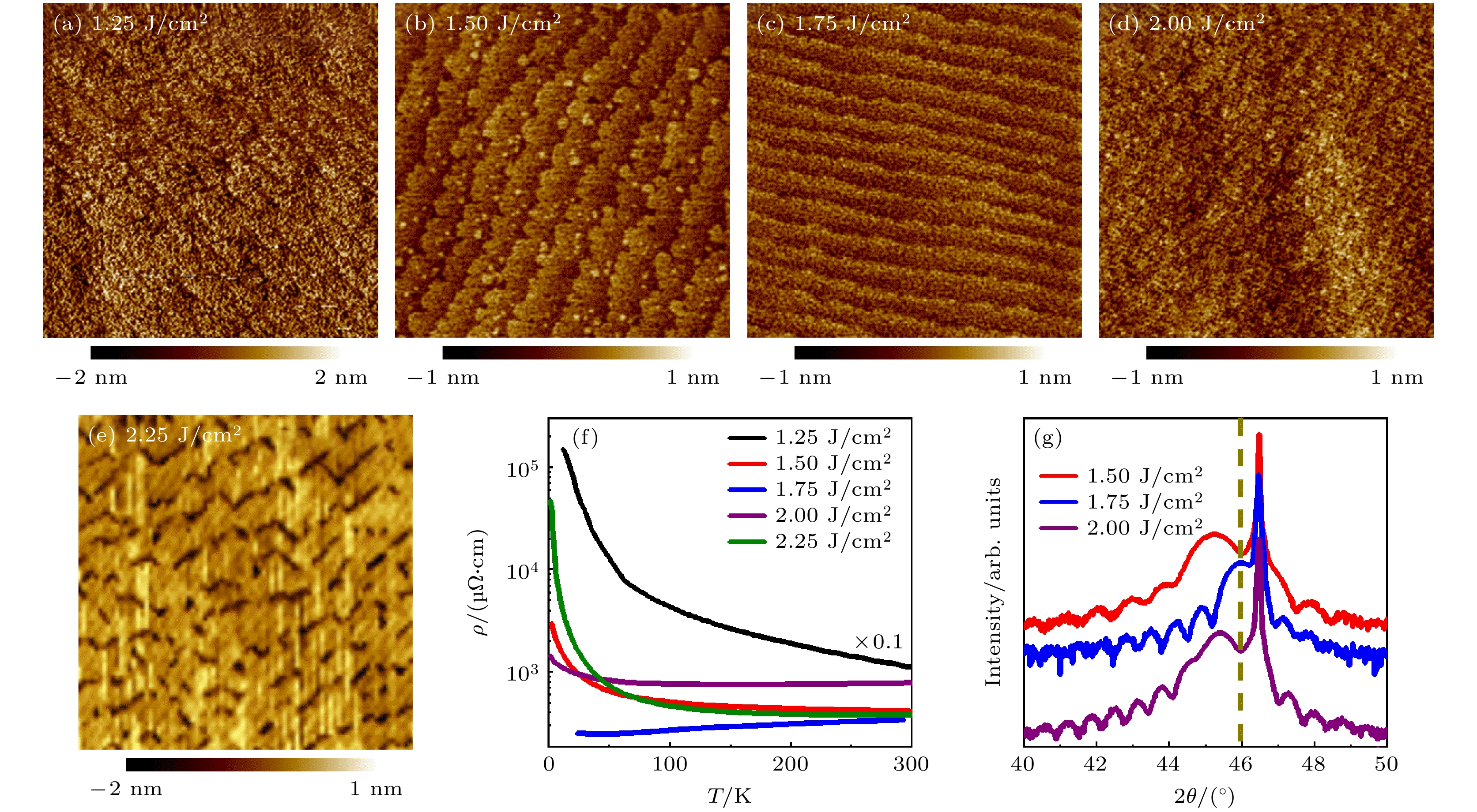
图 1 不同激光能量密度下生长的SRO薄膜表面形貌AFM图及电学性质和结构表征 (a)—(e)激光能量密度分别为1.25, 1.5, 1.75, 2和2.25 J/cm2时样品AFM图, 测试区域为2 μm × 2 μm, 薄膜厚度均为6个单胞; (f) 不同激光能量密度生长的薄膜电阻率随温度的变化, 其中1.25和2.25 J/cm2样品数据绘制在右坐标轴中; (g) 不同激光能量密度生长的薄膜的XRD图, 虚线为面外晶格常数c最小时SRO(002)峰位置
Figure 1. AFM images and resistivity of 6-unit-cell SRO thin films grown using different laser fluence: (a)–(e) AFM images of SRO thin film grown under 1.25, 1.5, 1.75, 2 and 2.25 J/cm2, the size is 2 μm× 2 μm, the film thickness is 6 unit cells. (f) Resistivity of each thin film as a function of temperature. (g) XRD patterns for SRO films deposited under various laser fluence, the dashed line indicates the SRO (002) peak position when the out-of-plane lattice constant c reaches the minimum.
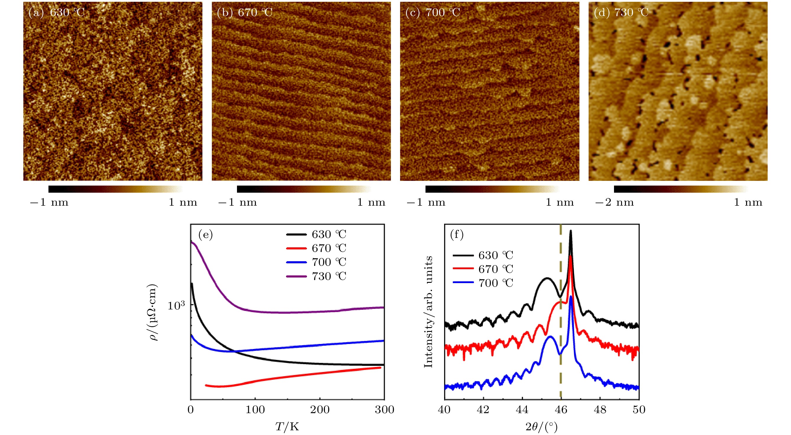
图 2 不同生长温度下生长的SRO薄膜表面形貌AFM图及电学性质表征 (a)—(d)生长温度分别为630, 670, 700和730 ℃下生长的薄膜表面AFM图, 区域为2 μm × 2 μm, 薄膜厚度均为6个单胞; (e)不同生长温度下生长的薄膜的电阻率随温度变化关系图; (f)不同生长温度下生长的薄膜其XRD图, 虚线为面外晶格常数c最小时SRO(002)峰位置
Figure 2. AFM images and resistivity of 6-unit-cell SRO thin films grown using different deposition temperature: (a)–(d) AFM images of SRO thin film grown at 630, 670, 700 and 730 ℃, the size is 2 μm × 2 μm, the film thickness is 6 unit cells. (e) Resistivity of each thin film as a function of temperature. (f) XRD patterns for SRO films deposited under various deposition temperature, the dashed line indicates the SRO (002) peak position when the out-of-plane lattice constant c reaches the minimum.
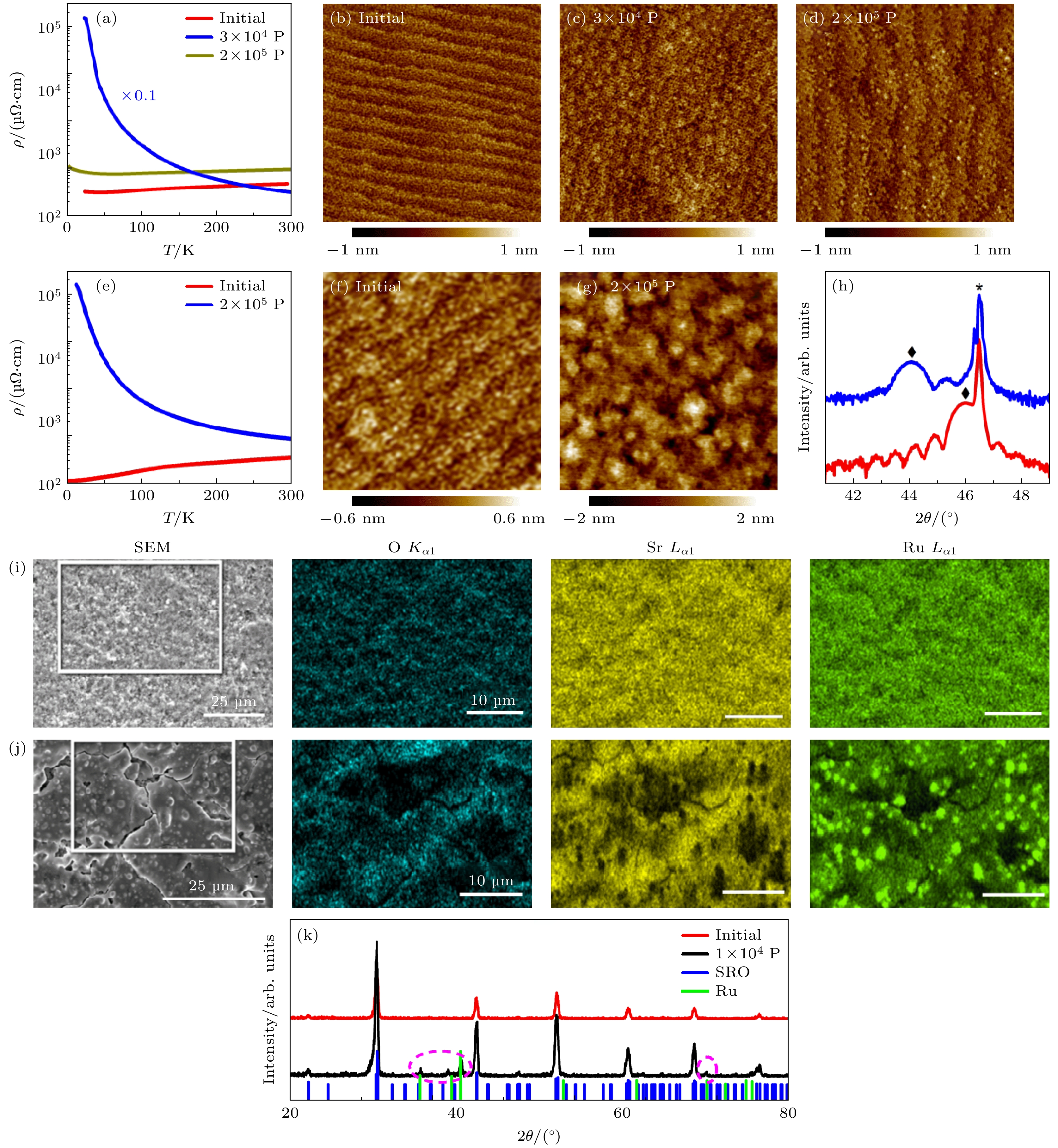
图 3 靶材表面经过不同激光脉冲数烧蚀后生长的SRO薄膜表面形貌和电学性质表征以及靶面SEM对比图 (a)—(d)磨靶后最初始生长及靶材分别经过3 × 10⁴ P和2 × 10⁵ P溅射后生长的薄膜电阻率随温度变化图(a)及表面形貌图(b)—(d), 厚度均为6个单胞, AFM测试区域为2 μm × 2 μm; (e)—(h)新鲜靶材和靶面经过2 × 10⁵ P溅射后生长的薄膜电阻率随温度变化图(e)、表面形貌图(f), (g)和XRD图(h), AFM测试区域为1 μm × 1 μm, (h)中*为衬底STO(002)峰, ♦为SRO(002)峰, 薄膜厚度为30个单胞; (i), (j)未经激光烧蚀与经过2 × 10⁵ P溅射后的SRO靶材表面SEM成像及EDS图; (k) 新鲜靶材、经过1 × 10⁴ P溅射后的靶面的XRD图以及SRO(蓝色)和Ru(绿色)的XRD标准卡片
Figure 3. AFM images and resistivity of SRO thin films grown after the target surface is ablated by different laser pulse numbers and SEM images of the target surface before and after laser ablation: (a)–(d) Resistivity and AFM images of the 6-unit-cell SRO thin films grown using fresh target and after the target is ablated by 3 × 10⁴ P and 2 × 10⁵ P, respectively. (e)–(h) Resistivity, AFM images and XRD patterns of the 30-unit-cell SRO thin films grown using fresh target and after the target is ablated by 2 × 10⁵ P, respectively. * denotes the (002) peak of STO while ♦ denotes the (002) peak of SRO in (h). (i), (j) SEM and EDS image of SRO target surface before and after 2 × 10⁵ P laser ablation; (k) XRD patterns for the fresh target, the ablated target with 2 × 10⁵ P, and the standard cards of SRO (blue) and Ru (green), respectively.
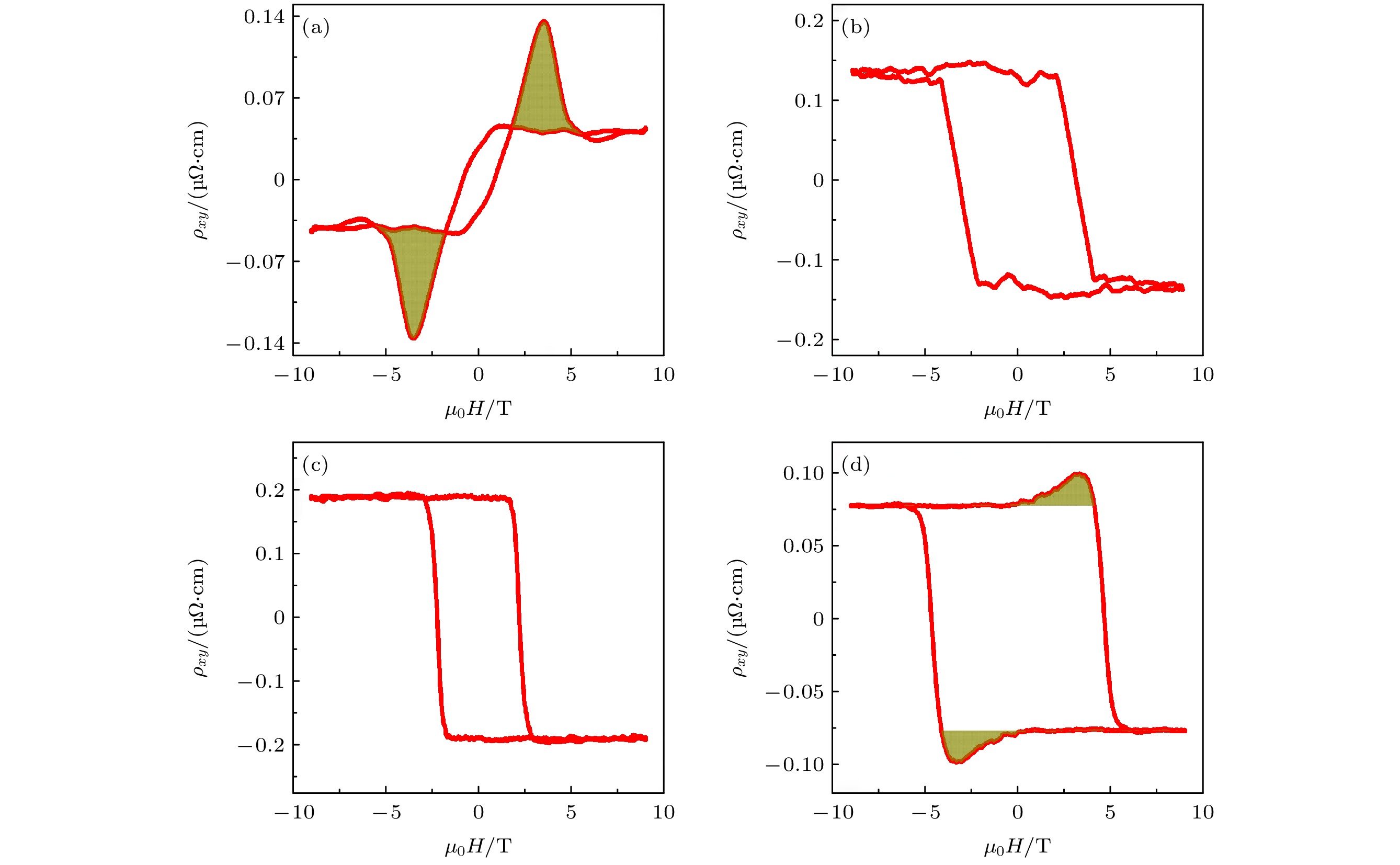
图 4 不同条件下生长的SRO薄膜在2 K时的霍尔效应表征 (a)最优生长条件; (b)激光能量密度为2.25 J/cm2; (c)生长温度为730 ℃; (d)靶材表面被预烧蚀3 × 10⁴ P
Figure 4. Hall resistivity of 6-unit-cell SRO grown under different conditions at 2 K. (a) The optimal growth conditions; (b) the laser fluence is 2.25 J/cm2; (c) the growth temperature is 730 ℃; (d) the target surface is ablated by 3 × 10⁴ P.
-
[1] Randall J J, Ward R 1959 J. Am. Chem. Soc. 81 2629
Google Scholar
[2] Mackenzie A P, Reiner J W, Tyler A W, Galvin L M, Julian S R, Beasley M R, Geballe T H, Kapitulnik A 1998 Phys. Rev. B 58 R13318
Google Scholar
[3] Klein L, Dodge J S, Ahn C H, Snyder G J, Geballe T H, Beasley M R, Kapitulnik A 1996 Phys. Rev. Lett. 77 2774
Google Scholar
[4] Maria J P, Trolier-McKinstry S, Schlom D G, Hawley M E, Brown G W 1998 J. Appl. Phys. 83 4373
Google Scholar
[5] Choi K J, Baek S H, Jang H W, Belenky L J, Lyubchenko M, Eom C B 2010 Adv. Mater. 22 759
Google Scholar
[6] Rijnders G, Blank D H A, Choi J, Eom C B 2004 Appl. Phys. Lett. 84 505
Google Scholar
[7] Choe H C, Kang T S, Je J H, Moon J H, Lee B T, Kim S S 2005 Thin Solid Films 474 44
Google Scholar
[8] Lee H N, Christen H M, Chisholm M F, Rouleau C M, Lowndes D H 2004 Appl. Phys. Lett. 84 4107
Google Scholar
[9] Sun Y, Zhong N, Zhang Y Y, Qi R J, Huang R, Tang X D, Yang P X, Xiang P H, Duan C G 2016 J. Appl. Phys. 120 235108
Google Scholar
[10] Toyota D, Ohkubo I, Kumigashira H, Oshima M, Ohnishi T, Lippmaa M, Kawasaki M, Koinuma H 2006 J. Appl. Phys. 99 08N505
Google Scholar
[11] Toyota D, Ohkubo I, Kumigashira H, Oshima M, Ohnishi T, Lippmaa M, Takizawa M, Fujimori A, Ono K, Kawasaki M, Koinuma H 2005 Appl. Phys. Lett. 87 162508
Google Scholar
[12] Shen X, Qiu X B, Su D, Zhou S Q, Li A D, Wu D 2015 J. Appl. Phys. 117 015307
Google Scholar
[13] Jeong H, Jeong S G, Mohamed A Y, Lee M, Noh W S, Kim Y, Bae J S, Choi W S, Cho D Y 2019 Appl. Phys. Lett. 115 092906
Google Scholar
[14] Chang Y J, Kim C H, Phark S H, Kim Y S, Yu J, Noh T W 2009 Phys. Rev. Lett. 103 057201
Google Scholar
[15] Matsuno J, Ogawa N, Yasuda K, Kagawa F, Koshibae W, Nagaosa N, Tokura Y, Kawasaki M 2016 Sci. Adv. 2 e1600304
Google Scholar
[16] Ohuchi Y, Matsuno J, Ogawa N, Kozuka Y, Uchida M, Tokura Y, Kawasaki M 2018 Nat. Commun. 9 213
Google Scholar
[17] Wang L F, Feng Q Y, Kim Y, Kim R, Lee K H, Pollard S D, Shin Y J, Zhou H B, Peng W, Lee D, Meng W J, Yang H, Han J H, Kim M, Lu Q Y, Noh T W 2018 Nat. Mater. 17 1087
Google Scholar
[18] Gu Y D, Wei Y W, Xu K, Zhang H R, Wan F, Li F, Saleem M S, Chang C Z, Sun J R, Song C, Feng J, Zhong X Y, Liu W, Zhang Z D, Zhu J, Pan F 2019 J. Phys. D:Appl. Phys. 52 404001
Google Scholar
[19] Wang W B, Daniels M W, Liao Z L, Zhao Y F, Wang J, Koster G, Rijnders G, Chang C Z, Xiao D, Wu W D 2019 Nat. Mater. 18 1054
Google Scholar
[20] Matl P, Ong N P, Yan Y F, Li Y Q, Studebaker D, Baum T, Doubinina G 1998 Phys. Rev. B 57 10248
Google Scholar
[21] Wang L, Feng Q, Lee H G, Ko E K, Lu Q, Noh T W 2020 Nano Lett. 20 2468
Google Scholar
[22] Kimbell G, Sass P M, Woltjes B, Ko E K, Noh T W, Wu W, Robinson J W A 2020 Phys. Rev. Mater. 4 054414
Google Scholar
[23] Lee S A, Oh S, Lee J, Hwang J Y, Kim J, Park S, Bae J S, Hong T E, Lee S, Kim S W, Kang W N, Choi W S 2017 Sci. Rep 7 11583
Google Scholar
[24] Ohnishi T, Lippmaa M, Yamamoto T, Meguro S, Koinuma H 2005 Appl. Phys. Lett. 87 241919
Google Scholar
[25] Keeble D J, Wicklein S, Dittmann R, Ravelli L, Mackie R A, Egger W 2010 Phys. Rev. Lett. 105 226102
Google Scholar
[26] Ohnishi T, Takada K 2011 Appl. Phys. Express 4 025501
Google Scholar
[27] Zhang J, Cheng L, Cao H, Bao M, Zhao J, Liu X, Zhao A, Choi Y, Zhou H, Shafer P, Zhai X 2022 Nano Res. 15 7584
Google Scholar
[28] Zakharov N D, Satyalakshmi K M, Koren G, Hesse D 1999 J. Mater. Res. 14 4385
Google Scholar
[29] Koster G, Klein L, Siemons W, Rijnders G, Dodge J S, Eom C B, Blank D H A, Beasley M R 2012 Rev. Mod. Phys. 84 253
Google Scholar
[30] Kaur P, Sharma K K, Pandit R, Choudhary R J, Kumar R 2014 Appl. Phys. Lett. 104 081608
Google Scholar
[31] Jia Q X, Chu F, Adams C D, Wu X D, Hawley M, Cho J H, Findikoglu A T, Foltyn S R, Smith J L, Mitchell T E 1996 J. Mater. Res. 11 2263
Google Scholar
[32] Jia Q X, Foltyn S R, Hawley M, Wu X D 1997 J. Vac. Sci. Technol. A 15 1080
[33] Shin J, Kalinin S V, Lee H N, Christen H M, Moore R G, Plummer E W, Baddorf A P 2005 Surf Sci. 581 118
Google Scholar
[34] Sohn B, Kim B, Choi J W, Chang S H, Han J H, Kim C 2020 Curr. Appl. Phys. 20 186
Google Scholar
[35] Kim G, Son K, Suyolcu Y E, Miao L, Schreiber N J, Nair H P, Putzky D, Minola M, Christiani G, van Aken P A, Shen K M, Schlom D G, Logvenov G, Keimer B 2020 Phys. Rev. Materials 4 104410
Google Scholar

 DownLoad:
Catalog
Metrics
- Abstract views: 2681
- PDF Downloads: 155
- Cited By: 0
