


-
As the characteristic size of the transistor approaches to its physical limit, the effect of impurities on device performance becomes more and more significant. The number of impurities and the range of impurity fluctuation become very limited in channel space less than 10 nm, and ionized impurities in local nano-space can even exhibit quantum dot characteristics, providing two discrete levels for charge transport. The behaviour of carrier tunnelling through quantum dots induced by ionized impurities can reveal the abundant quantum information, such as impurity ionization energy, coulomb interaction energy, electron activation energy, orbital level filling, and spin of local electrons. Quantum transport properties are also different in different doping concentrations because whether the quantum states overlap depends on the impurity atom spacing. The silicon nanostructure transistors using impurity atoms as building blocks of quantum transport are also called dopant atom transistors, which are not only compatible with complementary metal oxide semiconductor (CMOS) technology, but also expected to be the basic components of quantum computing circuits in the future. So far, their operating temperature is relatively low due to the shallow ground state energy level of impurity atoms. It is of great significance to study the quantum transport properties in dopant atom transistors and to observe quantum effects among them at room temperature. In this article, the quantum transport properties in single, discrete and coupled impurity atomic systems are described in detail by combining Anderson localization theory and Hubbard band model. Quantum transport in a discrete impurity atomic system is not only controlled by gate voltage, but also dependent on temperature. The current transport spectrum in the coupled impurity atomic system reveals more complex quantum dot characteristics. Single atom transistor can regulate quantum transport only by one impurity atom, which represents the ultimate scale limit of solid state devices. In addition, the methods of improving the operating temperature of dopant atom transistors are also systematically introduced, thereby laying a foundation for their practical applications.
-
Keywords:
- silicon nanostructure transistor /
- impurity atom /
- quantum transport /
- operating temperature
[1] Chan V, Rengarajan R, Rovedo N, Wei J 2003 Proceedings of IEEE International Electron Devices Meeting Washington USA, December 8−10, 2003 p381
[2] Mistry K, Allen C, Auth C 2007 Proceedings of IEEE International Electron Devices Meeting Washington USA, December 10−12, 2007 p247
[3] Auth C, Allen C, Blattner A 2012 Proceedings of Symposium on VLSI Technology Honolulu USA, June 12−14, 2012 p131
[4] Colinge J P, Lee C W, Afzalian A, Akhavan N D, Yan R, Ferain I, Razavi P, O’Neill B, Blake A, White M 2010 Nature Nanotech. 5 225
 Google Scholar
[5] Lee C W, Afzalian A, Akhavan N D, Yan R, Ferain I, Colinge J P 2009 Appl. Phys. Lett. 94 053511
Google Scholar
[6] 黎明, 黄如 2018 中国科学: 信息科学 48 963
Li M, Huang R 2018 Sci. Sin. Inform. 48 963
[7] Asenov A, Watling J R, Brown A R, Ferry D K 2002 J. Comput. Electron. 1 503
Google Scholar
[8] Taur Y 2002 IBM J. Res. Dev. 46 213
Google Scholar
[9] 李艳萍, 徐静平, 陈卫兵, 许胜国, 季峰 2006 物理学报 55 3670
Google Scholar
Li Y P, Xu J P, Chen W B, Xu S G, Ji F 2006 Acta Phys. Sin. 55 3670
Google Scholar
[10] 曹磊, 刘红侠 2012 物理学报 61 247303
Google Scholar
Cao L, Liu H X 2012 Acta Phys. Sin. 61 247303
Google Scholar
[11] Je M, Han S, Kim I, Shin H 2000 Solid-State Electron. 44 2207
Google Scholar
[12] Warren A C, Antoniadis D, Smith H I 1986 Phys. Rev. Lett. 56 1858
Google Scholar
[13] Rustagi S C, Singh N 2007 IEEE Electr. Device L. 28 909
Google Scholar
[14] Colinge J P, Xiong W 2006 IEEE Electr. Device L. 27 775
Google Scholar
[15] Park J T, Kim J Y 2010 Appl. Phys. Lett. 97 172101
Google Scholar
[16] Li Y M, Yu S M, Hwang J R, Yang F L 2008 IEEE Electr. Device L. 55 1449
Google Scholar
[17] Akhavan N D, Ferain I, Yu R, Razavi P, Colinge J P 2012 Solid-State Electron. 70 92
Google Scholar
[18] Ueda A, Luisier M, Sano N 2015 Appl. Phys. Lett. 107 253501
Google Scholar
[19] Zwanenburg F A, Dzurak A S, Morello A, Simmons M Y, Hollenberg L C L, Klimeck G, Rogge S, Coppersmith S N, Eriksson M A 2013 Rev. Mod. Phys. 85 0034
[20] Ryu H, Lee S, Fuechsle M, Miwa J A, Mahapatra S, Hollenberg L C L, Simmons M Y, Klimeck G 2015 Small 11 374
Google Scholar
[21] Moraru D, Udhiarto A, Anwar M, Nowak R, Jablonski R, Hamid E, Tarido J C, Mizuno T, Tabe M 2011 Nanoscale Res. Lett. 6 479
Google Scholar
[22] Moraru D, Ono Y, Inokawa H, Tabe M 2007 Phys. Rev. B 76 1
[23] Sellier H, Lansbergen G P, Caro J, Rogge S, Collaert N, Ferain I, Jurczak M, Biesemans S 2007 Appl. Phys. Lett. 90 3
[24] Barraud S, Berthomé M, Coquand R, Cassé M, Ernst T, Samson M P, Perreau P, Bourdelle K K, Faynot O, Poiroux T 2012 IEEE Electron. Device L. 33 1225
Google Scholar
[25] Moraru D, Tabe M 2013 Toward Quantum FinFET (Cham: Springer) pp305−324
[26] Tyryshkin A M, Tojo S, Morton J J L, Riemann H, Abrosimov N V, Becker P, Pohl H J, Schenkel T, Thewalt M L W, Itoh K M, Lyon S A 2012 Nature Mater. 11 143
Google Scholar
[27] Morello A, Pla J J, Zwanenburg F A, Chan K W, Tan K Y, Hubel H, Mttnen M, Nugroho C D, Yang C Y, van Donkelaar J A, Alves A D C, Jamieson D N, Escott C C, Hollenberg L C L, Clark R G, Dzurak A S 2010 Nature 467 687
Google Scholar
[28] Fuechsle M, Miwa J A, Mahapatra S, Ryu H, Lee S, Warschkow O, Hollenberg L C L, Klimeck G, Simmons Y M 2012 Nature Nanotech 7 242
Google Scholar
[29] Tabe M, Moraru D, Ligowski M, Anwar M, Jablonski R, Ono Y, Mizuno T 2010 Appl. Phys. Lett. 105 016803
Google Scholar
[30] Anwar M, Nowak R, Moraru D, Udhiarto A, Mizuno T, Jablonski R 2011 Appl. Phys. Lett. 99 213101
Google Scholar
[31] Tyszka K, Moraru D, Samanta A, Mizuno T, Jablonski R, Tabe M 2015 J. Appl. Phys. 117 244307
Google Scholar
[32] Lee P A, Fisher D S 1981 Phys. Rev. Lett. 47 882
Google Scholar
[33] 蒋祺, 龚昌德 1988 物理学报 37 941
Google Scholar
Jiang Q, Gong C D 1988 Acta Phys. Sin. 37 941
Google Scholar
[34] Mott N F, Twose W D, 1961 Adv. Phys. 10 107
Google Scholar
[35] Fleishman L, Licciardello D C, Anderson P W 1978 Phys. Rev. Lett. 40 1340
Google Scholar
[36] Yu D, Wang C J, Wehrenberg B L, Guyot-Sionnest P 2004 Phys. Rev. Lett. 92 216802
Google Scholar
[37] Mott N F 1968 J. Non-Cryst. Solids 1 1
Google Scholar
[38] Mott N F 1987 Conduction in Non-crystalline Materials (New York: Clarendon Press) p1
[39] Moraru D, Samanta A, Anh L T, Mizuno T, Mizuta H, Tabe M 2014 Sci. Rep. 4 6219
[40] Moraru D, Samanta A, Tyszka K, Anh L T, Muruganathan M, Mizuno T, Jablonski R, Mizuta H, Tabe M 2015 Nanoscale Res. Lett. 10 372
Google Scholar
[41] Wauqh F R, Berry M J, Crouch C H, Livermore C, Mar D J, Westervelt R M, Campman K L, Gossard A C 1996 Phys. Rev. B 53 1413
[42] Shinada T, Okamoto S, Kobayashi T, Ohdomari I 2005 Nature 437 1128
Google Scholar
[43] Anisimov V I, Zaanen J, Anderson O K 1991 Phys. Rev. B 44 943
Google Scholar
[44] Prati E, Hori M, Guagliardo F, Ferrari G, Shinada T 2012 Nature Nanotech. 7 443
Google Scholar
[45] Prati E, Kumagai K, Hori M, Shinada T 2015 Sci. Rep. 6 19704
[46] Shin S J, Lee J J, Kang H J, Choi J B, Yang S R E, Takahashi Y, Hasko D G 2011 Nano Lett. 11 1591
Google Scholar
[47] Tan Y, Kamiya T, Durrani Z A, Ahmed H 2003 J. Appl. Phys. 94 663
[48] Rafiq M A, Masubuchi K, Durrani Z A K, Colli A, Mizuta H, Milne W I, Oda S 2012 J. Appl. Phys. 51 025202
Google Scholar
[49] Saitoh M, Hiramoto T 2004 Appl. Phys. Lett. 84 3172
Google Scholar
[50] Deshpande V, Barraud S, Jehl X, Wacquez R, Vinet M, Coquand R, Roche B, Voisin B, Triozon F, Vizioz C 2013 Solid-State Electron. 84 179
Google Scholar
[51] Lavieville R, Triozon F, Barraud S, Corna A, Jehl X, Sanquer M, Li J, Abisset A, Duchemin I, Niquet Y M 2015 Nano Lett. 15 2958
Google Scholar
[52] Lee S, Lee Y, Song E B, Hiramoto T 2014 Nano Lett. 14 71
Google Scholar
[53] Tabe M, Samanta A, Moraru D 2017 Recent Global Research and Education: Technological Challenges (Cham: Springer) p83
[54] Björk M T, Schmid H, Knoch J, Riel H, Riess W 2008 Nature Nanotech. 4 103
[55] Diarra M, Niquet Y M, Delerue C, Allan G 2007 Phys. Rev. B 75 045301
Google Scholar
[56] Pierre M, Wacquez R, Sanquer M, Vinet M, Cueto O 2009 Nature Nanotech. 5 133
[57] Hamid E, Moraru D, Kuzuya Y, Mizuno T, Anh L T, Mizuta H, Tabe M 2013 Phys. Rev. B 87 085420
Google Scholar
[58] Samanta A, Muruganathan M, Hori M, Ono Y, Mizuta H, Tabe M, Moraru D 2017 Appl. Phys. Lett. 110 093107
Google Scholar
[59] Matveev K A, Glazman L I 1996 Phys. Rev. B 54 10339
Google Scholar
[60] Tamura H, Takahashi Y, Murase K 1999 Microelectron. Eng. 47 205
Google Scholar
[61] Morgan N Y, Abusch-Magder D, Kastner M A, Takahashi Y, Tamura H, Murase K 2001 J. Appl. Phys. 89 410
Google Scholar
[62] Durrani Z, Jones M, Abualnaja F, Wang C, Kaestner M, Lenk S, Lenk C, Rangelow W L, Andreev A 2018 J. Appl. Phys. 124 144502
Google Scholar
[63] Klein M, Lansbergen G P, Mol J A, Rogge S, Levine R D, Remacle F 2009 ChemPhysChem 10 162
Google Scholar
[64] Klein M, Mol J A, Verduijn J, Lansbergen G P, Rogge S, Levine R D, Remacle F 2010 Appl. Phys. Lett. 96 043107
Google Scholar
[65] Fresch B, Bocquel J, Hiluf D, Rogge S, Levine R D, Remacle F 2017 ChemPhysChem 18 1790
Google Scholar
-
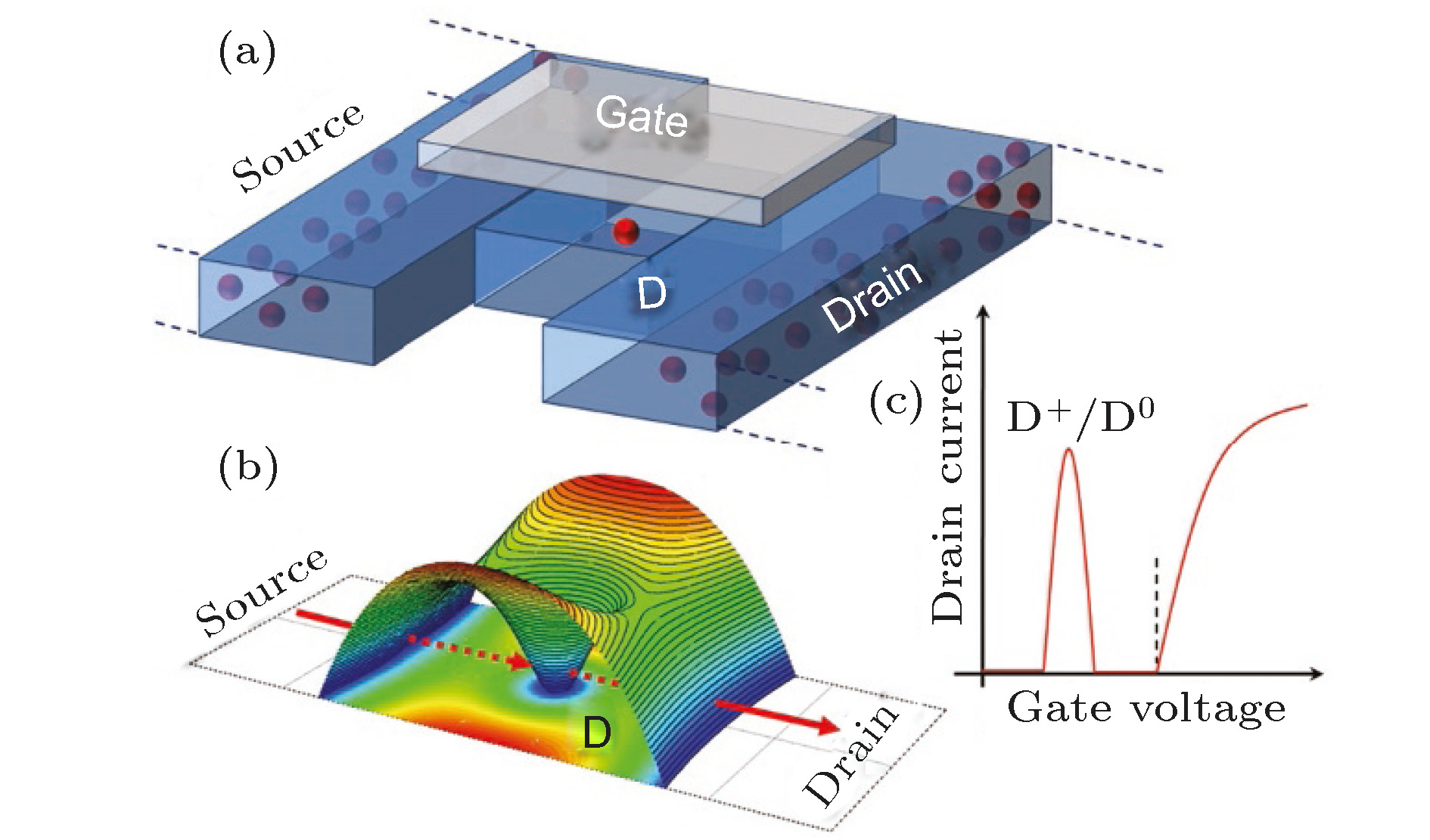
图 2 理想单杂质晶体管的基本结构和工作原理图 (a)单杂质晶体管结构示意图; (b)施主原子调制源端到漏端的单电子隧穿; (c)低温下单杂质晶体管的转移特性曲线[25]
Figure 2. Structure and schematic diagram of the ideal single-dopant transistor: (a) Schematic illustration of single-dopant transistor; (b) donor mediates single-electron tunneling from source to drain; (c) transfer characteristics for single-dopant transistor in the low temperature[25].
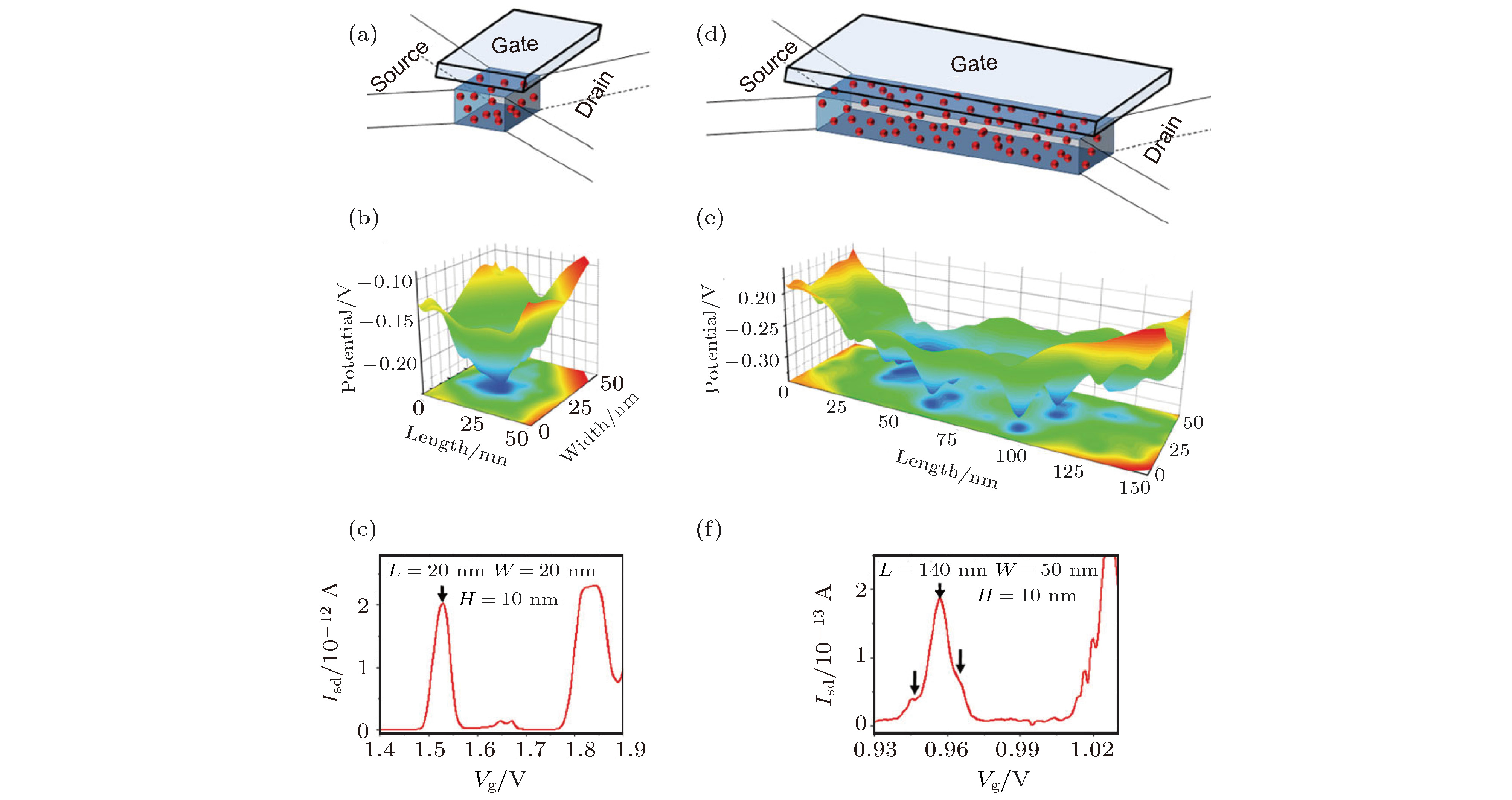
图 4 (a)短沟道器件示意图; (b)短沟道器件电势分布图; (c)短沟道器件Isd -Vg特性曲线(Vsd = 5 mV); (d)长沟道器件示意图; (e)长沟道器件电势分布图; (f)长沟道器件Isd -Vg特性曲线(Vsd = 5 mV)[29]
Figure 4. (a) Schematic channel structure; (b) example of simulated potential profile; (c) example of dc Isd -Vg characteristics (Vsd = 5 mV) for a short-channel FET; (d) schematic channel structure; (e) example of simulated potential profile; (f) example of dc Isd -Vg chara-cteristics (Vsd = 5 mV) for a long-channel FET[29].

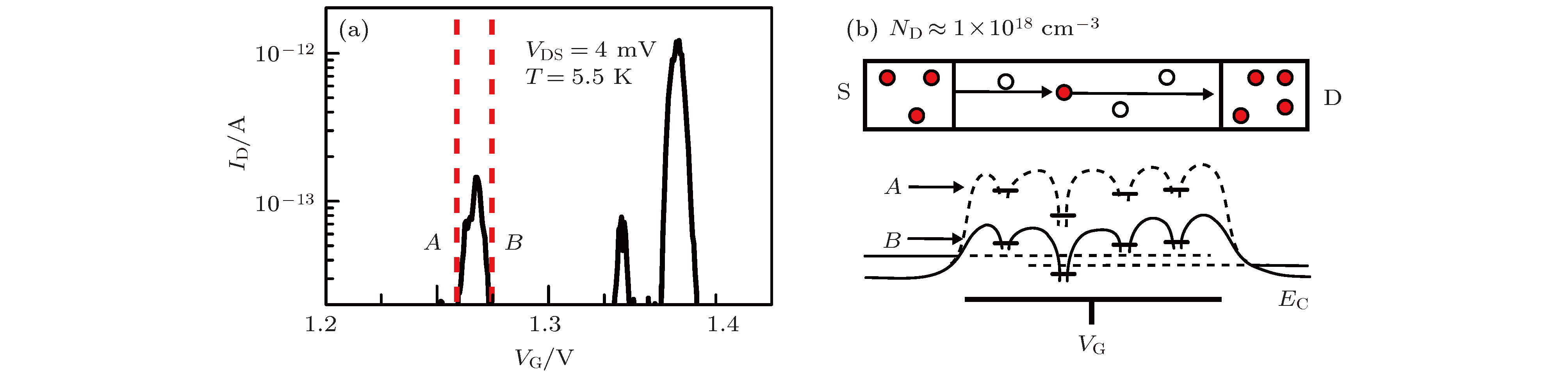


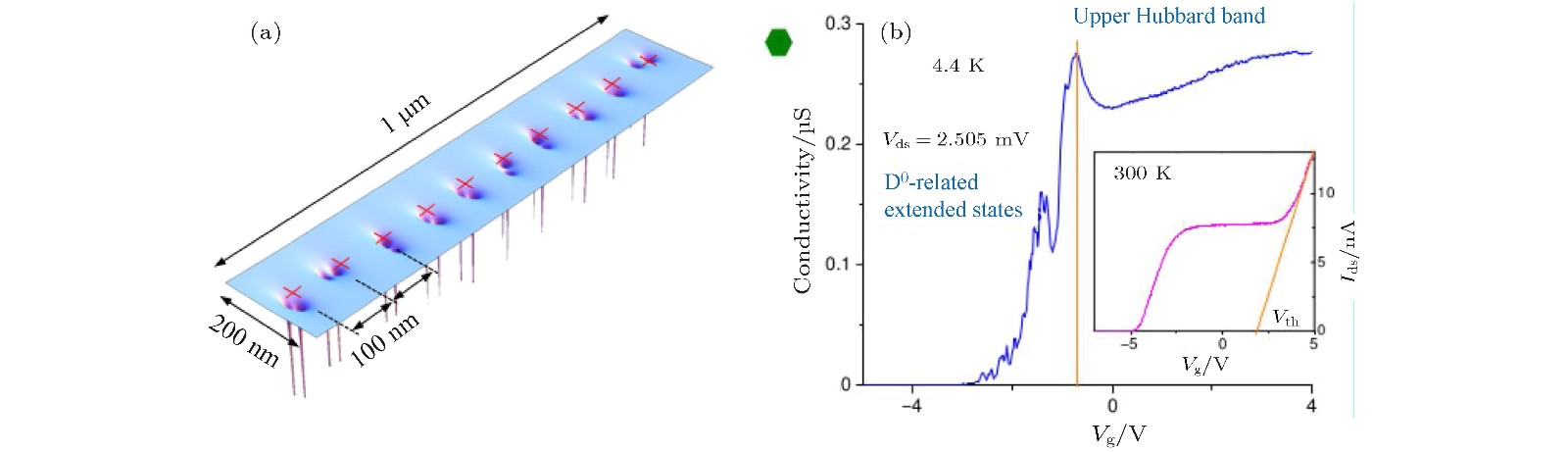
图 15 (a)沿沟道分布的20个磷施主原子中电势分布的理想示意图; (b)Vds = 2.505 mV时, 在4.4 K下测量的器件电导-栅压曲线. 插图: Vds = 2.505 mV时, 室温下提取的阈值电压[45]
Figure 15. (a) An idealized representation of the potential distributions in the 20 phosphorous donors distributed along the channel of the sample; (b) conductance σ of the device probed at 4.4 K measured at Vds = 2.505 mV. Inlet: extraction of the threshold voltage at room temperature, at Vds = 2.505 mV[45].
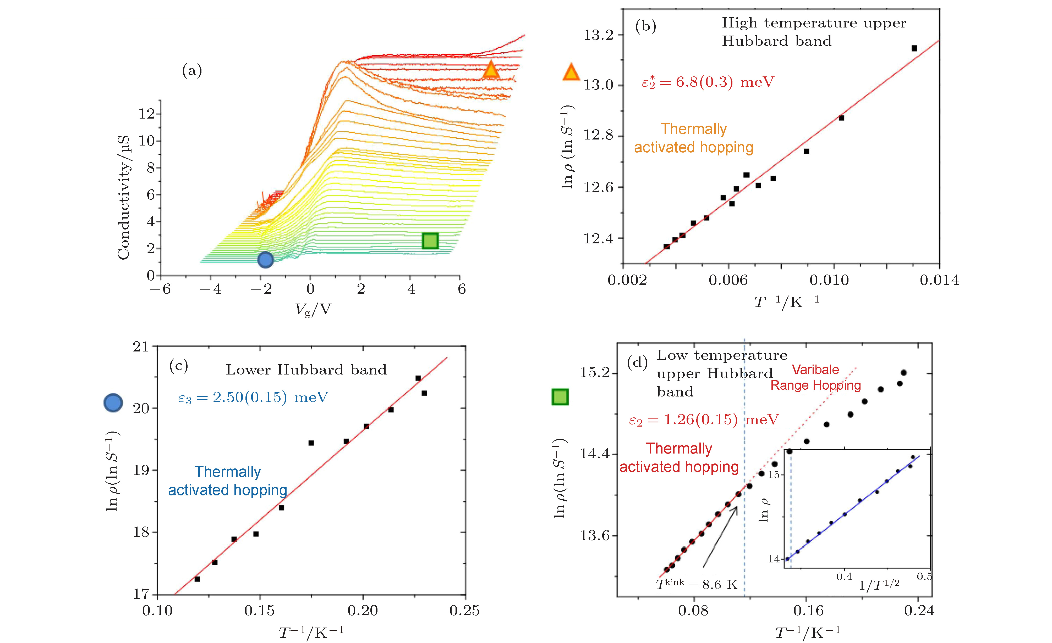
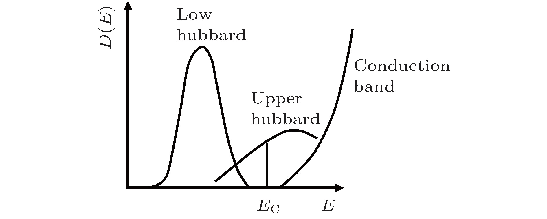
图 16 (a)4.2—274 K温度区间下的电导-栅压曲线; (b)高温下上Hubbard带的热激活输运; (c)低温下下Hubbard带的热激活输运; (d)低温下上Hubbard带的热激活输运[45]
Figure 16. (a) The conductance as a function of the gate voltage Vg from 4.2 to 274 K; (b) the thermal activation of the upper Hubbard band at high temperature; (c) the thermal activation of the lower Hubbard band at low temperature; (d) the thermal activation of the upper Hubbard band at low temperature[45].
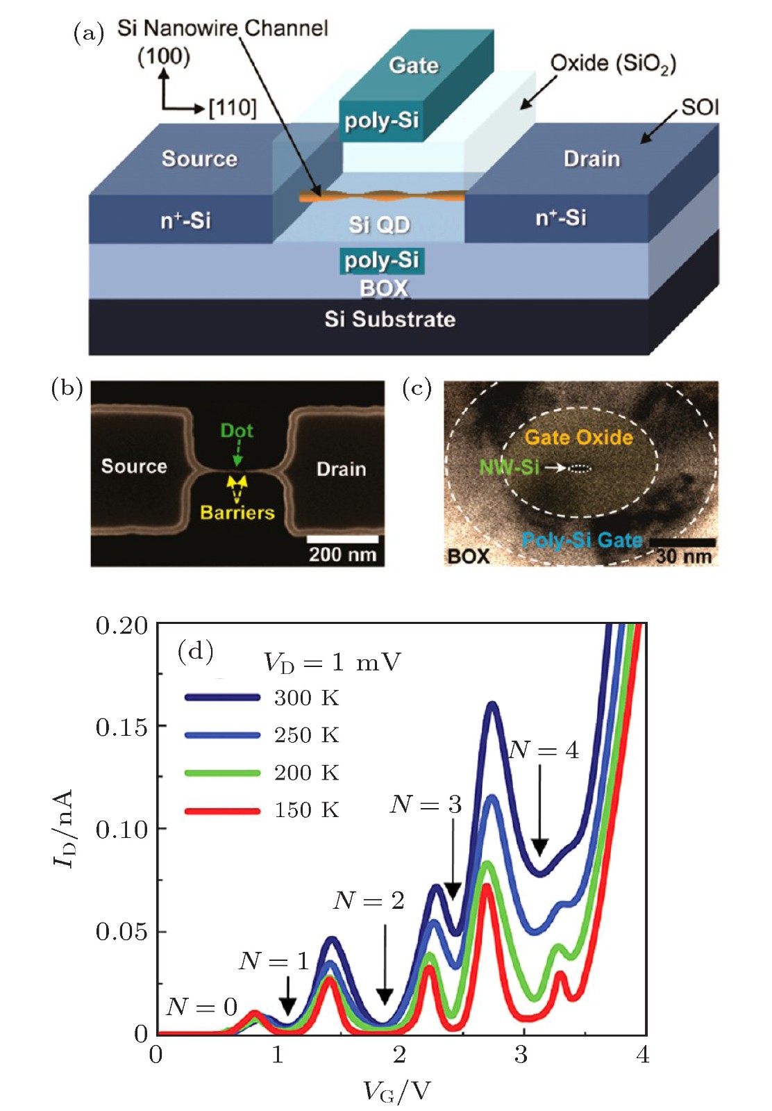
图 17 (a)单电子晶体管结构示意图; (b)化学湿法腐蚀后硅纳米线扫描电子显微镜(SEM)图; (c)形成围栅GAA结构后硅纳米线透射电子显微镜(TEM)图; (d)制备的单电子晶体管在150−300 K下的ID-VG特性曲线[52]
Figure 17. (a) Schematic configuration of the fabricated Si SET; (b) scanning electron microscopy image of the Si nanowire after chemical wet-etching; (c) transmission electron microscopy image of the Si nanowire after fabricating the GAA structure; (d) ID−VG characteristic curves of the fabricated SET at T = 150−300 K[52].


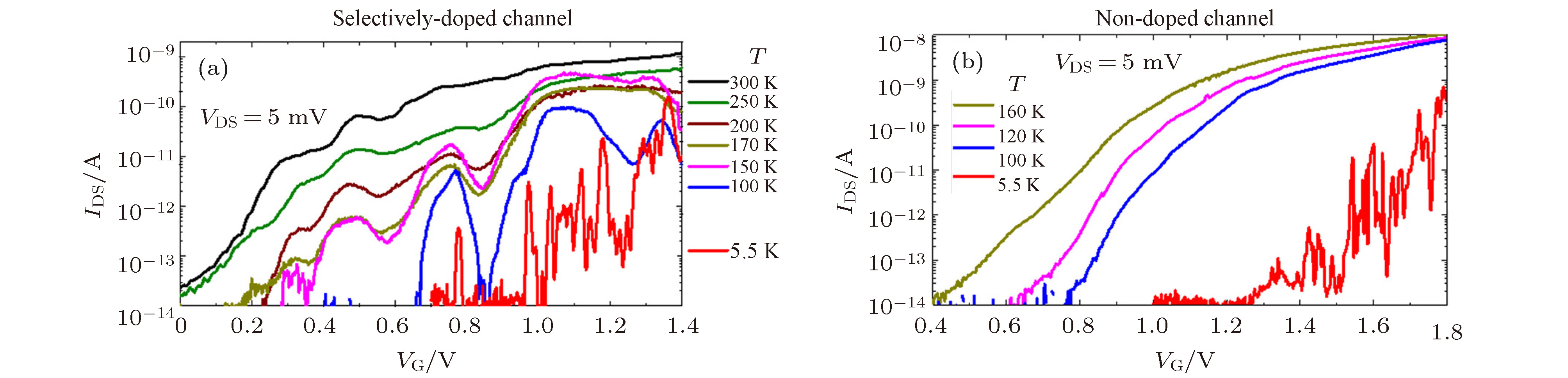
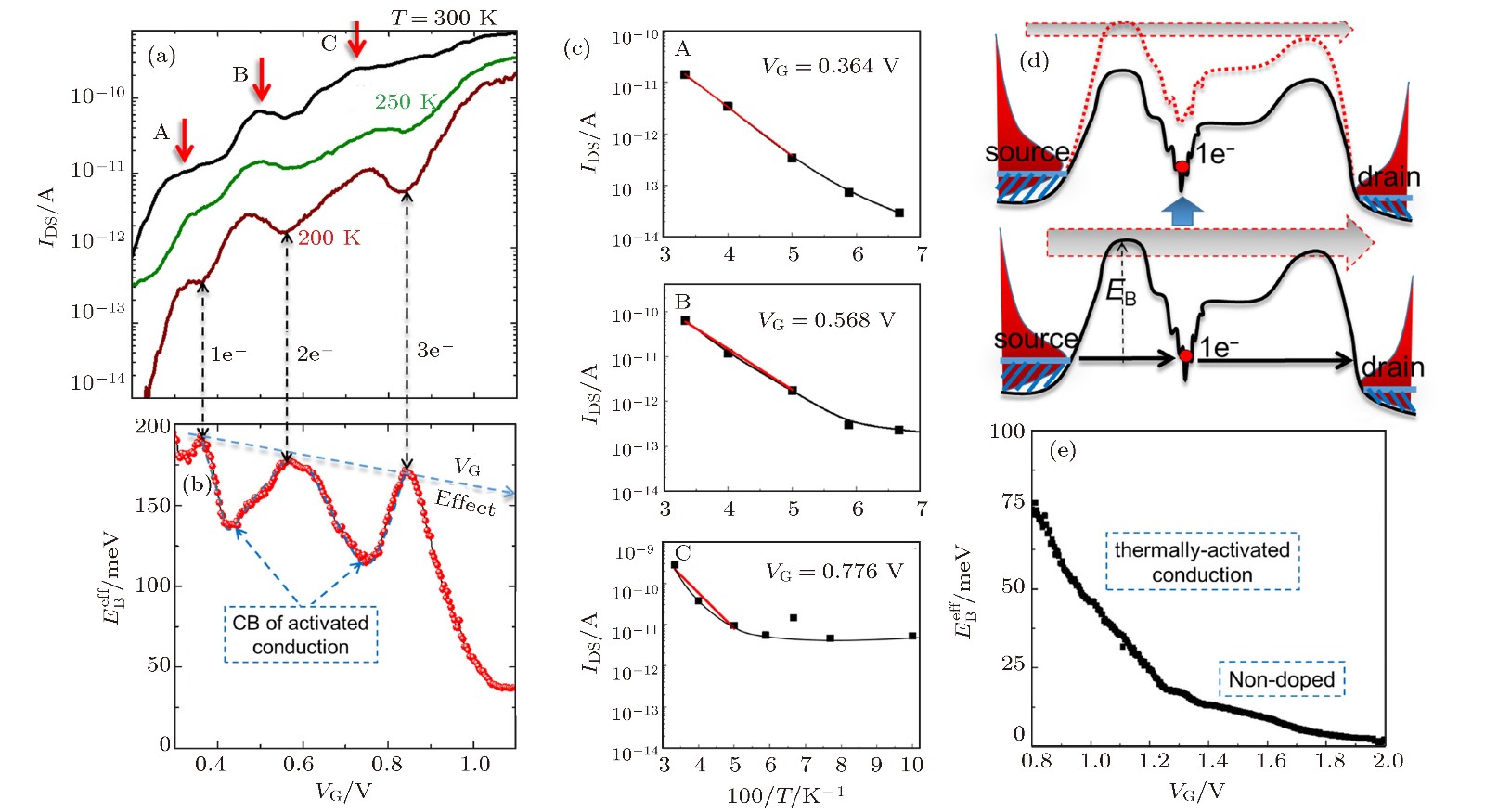
图 25 (a)不同温度下, 沟道选择性掺杂SOI-FET器件IDS-VG特性曲线; (b)有效势垒高度随栅压VG的变化; (c)不同电流峰对应的Arrhenius曲线; (d)激活传导的库仑阻塞机制(下图), 量子点俘获电子的库仑阻塞情形(上图); (e)沟道未掺杂SOI-FET器件仅仅表现出热激活传导性质[58]
Figure 25. (a) IDS-VG characteristics as a function of temperature for the selectively-doped channel SOI-FET; (b) effective barrier height (EBeff) estimated from Arrhenius plots as a function of VG; (c) arrhenius plots for VG corresponding to different peaks; (d) schematic illustrations of the mechanism of Coulomb blockade of activated conduction for the single-electron tunneling current peak (lower panel) and for the Coulomb blockade condition with an electron trapped in the QD (upper panel); (e) EBeff extracted for a non-doped-channel SOI-FET, exhibiting only behavior typical of thermally-activated conduction[58].
-
[1] Chan V, Rengarajan R, Rovedo N, Wei J 2003 Proceedings of IEEE International Electron Devices Meeting Washington USA, December 8−10, 2003 p381
[2] Mistry K, Allen C, Auth C 2007 Proceedings of IEEE International Electron Devices Meeting Washington USA, December 10−12, 2007 p247
[3] Auth C, Allen C, Blattner A 2012 Proceedings of Symposium on VLSI Technology Honolulu USA, June 12−14, 2012 p131
[4] Colinge J P, Lee C W, Afzalian A, Akhavan N D, Yan R, Ferain I, Razavi P, O’Neill B, Blake A, White M 2010 Nature Nanotech. 5 225
Google Scholar
[5] Lee C W, Afzalian A, Akhavan N D, Yan R, Ferain I, Colinge J P 2009 Appl. Phys. Lett. 94 053511
Google Scholar
[6] 黎明, 黄如 2018 中国科学: 信息科学 48 963
Li M, Huang R 2018 Sci. Sin. Inform. 48 963
[7] Asenov A, Watling J R, Brown A R, Ferry D K 2002 J. Comput. Electron. 1 503
Google Scholar
[8] Taur Y 2002 IBM J. Res. Dev. 46 213
Google Scholar
[9] 李艳萍, 徐静平, 陈卫兵, 许胜国, 季峰 2006 物理学报 55 3670
Google Scholar
Li Y P, Xu J P, Chen W B, Xu S G, Ji F 2006 Acta Phys. Sin. 55 3670
Google Scholar
[10] 曹磊, 刘红侠 2012 物理学报 61 247303
Google Scholar
Cao L, Liu H X 2012 Acta Phys. Sin. 61 247303
Google Scholar
[11] Je M, Han S, Kim I, Shin H 2000 Solid-State Electron. 44 2207
Google Scholar
[12] Warren A C, Antoniadis D, Smith H I 1986 Phys. Rev. Lett. 56 1858
Google Scholar
[13] Rustagi S C, Singh N 2007 IEEE Electr. Device L. 28 909
Google Scholar
[14] Colinge J P, Xiong W 2006 IEEE Electr. Device L. 27 775
Google Scholar
[15] Park J T, Kim J Y 2010 Appl. Phys. Lett. 97 172101
Google Scholar
[16] Li Y M, Yu S M, Hwang J R, Yang F L 2008 IEEE Electr. Device L. 55 1449
Google Scholar
[17] Akhavan N D, Ferain I, Yu R, Razavi P, Colinge J P 2012 Solid-State Electron. 70 92
Google Scholar
[18] Ueda A, Luisier M, Sano N 2015 Appl. Phys. Lett. 107 253501
Google Scholar
[19] Zwanenburg F A, Dzurak A S, Morello A, Simmons M Y, Hollenberg L C L, Klimeck G, Rogge S, Coppersmith S N, Eriksson M A 2013 Rev. Mod. Phys. 85 0034
[20] Ryu H, Lee S, Fuechsle M, Miwa J A, Mahapatra S, Hollenberg L C L, Simmons M Y, Klimeck G 2015 Small 11 374
Google Scholar
[21] Moraru D, Udhiarto A, Anwar M, Nowak R, Jablonski R, Hamid E, Tarido J C, Mizuno T, Tabe M 2011 Nanoscale Res. Lett. 6 479
Google Scholar
[22] Moraru D, Ono Y, Inokawa H, Tabe M 2007 Phys. Rev. B 76 1
[23] Sellier H, Lansbergen G P, Caro J, Rogge S, Collaert N, Ferain I, Jurczak M, Biesemans S 2007 Appl. Phys. Lett. 90 3
[24] Barraud S, Berthomé M, Coquand R, Cassé M, Ernst T, Samson M P, Perreau P, Bourdelle K K, Faynot O, Poiroux T 2012 IEEE Electron. Device L. 33 1225
Google Scholar
[25] Moraru D, Tabe M 2013 Toward Quantum FinFET (Cham: Springer) pp305−324
[26] Tyryshkin A M, Tojo S, Morton J J L, Riemann H, Abrosimov N V, Becker P, Pohl H J, Schenkel T, Thewalt M L W, Itoh K M, Lyon S A 2012 Nature Mater. 11 143
Google Scholar
[27] Morello A, Pla J J, Zwanenburg F A, Chan K W, Tan K Y, Hubel H, Mttnen M, Nugroho C D, Yang C Y, van Donkelaar J A, Alves A D C, Jamieson D N, Escott C C, Hollenberg L C L, Clark R G, Dzurak A S 2010 Nature 467 687
Google Scholar
[28] Fuechsle M, Miwa J A, Mahapatra S, Ryu H, Lee S, Warschkow O, Hollenberg L C L, Klimeck G, Simmons Y M 2012 Nature Nanotech 7 242
Google Scholar
[29] Tabe M, Moraru D, Ligowski M, Anwar M, Jablonski R, Ono Y, Mizuno T 2010 Appl. Phys. Lett. 105 016803
Google Scholar
[30] Anwar M, Nowak R, Moraru D, Udhiarto A, Mizuno T, Jablonski R 2011 Appl. Phys. Lett. 99 213101
Google Scholar
[31] Tyszka K, Moraru D, Samanta A, Mizuno T, Jablonski R, Tabe M 2015 J. Appl. Phys. 117 244307
Google Scholar
[32] Lee P A, Fisher D S 1981 Phys. Rev. Lett. 47 882
Google Scholar
[33] 蒋祺, 龚昌德 1988 物理学报 37 941
Google Scholar
Jiang Q, Gong C D 1988 Acta Phys. Sin. 37 941
Google Scholar
[34] Mott N F, Twose W D, 1961 Adv. Phys. 10 107
Google Scholar
[35] Fleishman L, Licciardello D C, Anderson P W 1978 Phys. Rev. Lett. 40 1340
Google Scholar
[36] Yu D, Wang C J, Wehrenberg B L, Guyot-Sionnest P 2004 Phys. Rev. Lett. 92 216802
Google Scholar
[37] Mott N F 1968 J. Non-Cryst. Solids 1 1
Google Scholar
[38] Mott N F 1987 Conduction in Non-crystalline Materials (New York: Clarendon Press) p1
[39] Moraru D, Samanta A, Anh L T, Mizuno T, Mizuta H, Tabe M 2014 Sci. Rep. 4 6219
[40] Moraru D, Samanta A, Tyszka K, Anh L T, Muruganathan M, Mizuno T, Jablonski R, Mizuta H, Tabe M 2015 Nanoscale Res. Lett. 10 372
Google Scholar
[41] Wauqh F R, Berry M J, Crouch C H, Livermore C, Mar D J, Westervelt R M, Campman K L, Gossard A C 1996 Phys. Rev. B 53 1413
[42] Shinada T, Okamoto S, Kobayashi T, Ohdomari I 2005 Nature 437 1128
Google Scholar
[43] Anisimov V I, Zaanen J, Anderson O K 1991 Phys. Rev. B 44 943
Google Scholar
[44] Prati E, Hori M, Guagliardo F, Ferrari G, Shinada T 2012 Nature Nanotech. 7 443
Google Scholar
[45] Prati E, Kumagai K, Hori M, Shinada T 2015 Sci. Rep. 6 19704
[46] Shin S J, Lee J J, Kang H J, Choi J B, Yang S R E, Takahashi Y, Hasko D G 2011 Nano Lett. 11 1591
Google Scholar
[47] Tan Y, Kamiya T, Durrani Z A, Ahmed H 2003 J. Appl. Phys. 94 663
[48] Rafiq M A, Masubuchi K, Durrani Z A K, Colli A, Mizuta H, Milne W I, Oda S 2012 J. Appl. Phys. 51 025202
Google Scholar
[49] Saitoh M, Hiramoto T 2004 Appl. Phys. Lett. 84 3172
Google Scholar
[50] Deshpande V, Barraud S, Jehl X, Wacquez R, Vinet M, Coquand R, Roche B, Voisin B, Triozon F, Vizioz C 2013 Solid-State Electron. 84 179
Google Scholar
[51] Lavieville R, Triozon F, Barraud S, Corna A, Jehl X, Sanquer M, Li J, Abisset A, Duchemin I, Niquet Y M 2015 Nano Lett. 15 2958
Google Scholar
[52] Lee S, Lee Y, Song E B, Hiramoto T 2014 Nano Lett. 14 71
Google Scholar
[53] Tabe M, Samanta A, Moraru D 2017 Recent Global Research and Education: Technological Challenges (Cham: Springer) p83
[54] Björk M T, Schmid H, Knoch J, Riel H, Riess W 2008 Nature Nanotech. 4 103
[55] Diarra M, Niquet Y M, Delerue C, Allan G 2007 Phys. Rev. B 75 045301
Google Scholar
[56] Pierre M, Wacquez R, Sanquer M, Vinet M, Cueto O 2009 Nature Nanotech. 5 133
[57] Hamid E, Moraru D, Kuzuya Y, Mizuno T, Anh L T, Mizuta H, Tabe M 2013 Phys. Rev. B 87 085420
Google Scholar
[58] Samanta A, Muruganathan M, Hori M, Ono Y, Mizuta H, Tabe M, Moraru D 2017 Appl. Phys. Lett. 110 093107
Google Scholar
[59] Matveev K A, Glazman L I 1996 Phys. Rev. B 54 10339
Google Scholar
[60] Tamura H, Takahashi Y, Murase K 1999 Microelectron. Eng. 47 205
Google Scholar
[61] Morgan N Y, Abusch-Magder D, Kastner M A, Takahashi Y, Tamura H, Murase K 2001 J. Appl. Phys. 89 410
Google Scholar
[62] Durrani Z, Jones M, Abualnaja F, Wang C, Kaestner M, Lenk S, Lenk C, Rangelow W L, Andreev A 2018 J. Appl. Phys. 124 144502
Google Scholar
[63] Klein M, Lansbergen G P, Mol J A, Rogge S, Levine R D, Remacle F 2009 ChemPhysChem 10 162
Google Scholar
[64] Klein M, Mol J A, Verduijn J, Lansbergen G P, Rogge S, Levine R D, Remacle F 2010 Appl. Phys. Lett. 96 043107
Google Scholar
[65] Fresch B, Bocquel J, Hiluf D, Rogge S, Levine R D, Remacle F 2017 ChemPhysChem 18 1790
Google Scholar

 DownLoad:

Catalog
Metrics
- Abstract views: 23139
- PDF Downloads: 125
- Cited By: 0
