


-
Vertical cavity surface emitting lasers (VCSELs) are widely used in the field of short-range optical communication and optical interconnection because of their advantages such as low threshold current, large modulation bandwidth, easy two-dimensional integration, easy coupling with optical fibers and low cost. The VCSELs and heterojunction bipolar transistor (HBT) are longitudinal current devices, so they can be well integrated on the same wafer, and the output light power can be modulated by the HBT base current. Integration of VCSELs and HBT are designed in this paper. The VCSELs and PNP InGaP/GaAs HBT form a direct series structure. The reflectivity of DBR is 99.72% at a resonant wavelength of 850 nm and 99.57% after adding HBT separately. Therefore, the addition of HBT has little influence on the reflectivity of DBR at the resonant wavelength. The electro-optical characteristics of the integrated structure are simulated by using PICS3D software. An interim collector is added into the model in order to ensure that the simulation can be carried out smoothly. Firstly, HBT is conducted and the current flows from the emitter to the interim collector. Then, the voltage across the interim collector and the N-type electrode is increased to make VCSELs conducted and the current of the transition collector drop to zero. The interim collector can be removed from the actual structure because the current is zero. The simulation results show that the current gain coefficient is 400, and the maximum modulation rate of the base current to the output light power rises up to 280 mW/mA. The maximum temperature in the active region increases with the base current increasing, and the output light power first increases and then tends to be saturated. The ac optical gain characteristics of the integrated structure is simulated by PICS3D, and the simulation result shows that cutoff frequency exceeds 1 GHz. The addition of HBT limits the modulation rate of the integrated structure, and further optimization of HBT structure parameters and geometric dimension are needed to improve the modulation rate. The integrated structure and simulation method established in this paper can also be used to integrate LED, LD, DFB or other luminescent devices with HBT.
-
Keywords:
- vertical cavity surface emitting lasers /
- heterojunction bipolar transistor /
- opto-electronic integrated circuits
[1] 张星, 张奕, 张建伟, 张建, 钟础宇, 黄佑文, 宁永强, 顾思洪, 王立军 2016 物理学报 65 134204
 Google Scholar
Zhang X, Zhang Y, Zhang J W, Zhang J, Zhong C Y, Huang Y W, Ning Y Q, Gu S H, Wang L J 2016 Acta Phys. Sin. 65 134204
Google Scholar
[2] 郝永芹, 冯源, 王菲, 晏长岭, 赵英杰, 王晓华, 王玉霞, 姜会林, 高欣, 薄报学 2011 物理学报 60 064201
Hao Y Q, Feng Y, Wang F, Yan C L, Zhao Y J, Wang X H, Wang Y X, Jiang H L, Gao X, Bao B X 2011 Acta Phys. Sin. 60 064201
[3] 彭红玲, 韩勤, 杨晓红, 牛智川 2006 物理学报 56 863
Peng H L, Han Q, Yang X H, Niu Z C 2006 Acta Phys. Sin. 56 863
[4] 杨威, 刘训春, 朱旻, 王润梅, 申华军 2006 半导体学报 27 1603
Yang W, Liu X C, Zhu M, Wang R M, Shen H J 2006 Chin. J. Semicond. 27 1603
[5] Mishra U K, Singh J 2008 Semiconductor Device Physics and Design (Dordrecht: Springer) p246
[6] Liu X, Yuan J S, Liou J J 2008 Microelectron. Reliab. 48 1212
Google Scholar
[7] Zhou P, Cheng J L, Zolper J C, Lear K L, Chalmers S A, Vawter G A, Leibenguth R E, Adams A C 1993 IEEE Photonic. Tech. L. 5 1035
Google Scholar
[8] Berger P R, Dutta N K, Sivco D L, Cho A Y 1991 Appl. Phys. Lett. 59 2826
Google Scholar
[9] Feng M, Qiu J Y, Holonyak N 2018 IEEE J. Quantum Elect. 54 2000514
[10] Shi W, Faraji B, Greenberg M, Berggren J, Xiang Y, Hammar M, Lestrade M, Li Z Q, Li Z M S, Chrostowski L 2011 Opt. Quant. Electron. 42 659
Google Scholar
[11] Xiang Y, Hedlund C R, Yu X, Yang C, Zabel T, Hammar M, Akram M N 2015 J Opt. Soc. Am. 23 15680
[12] Kuchta D M, Rylyakov A V, Doany F E, Schow C L, Proesel J, Baks C W, Westbergh P, Gustavsson J S, Larsson A 2015 IEEE Photonic Tech. L. 27 577
Google Scholar
[13] Kishi T, Nagatani M, Kanazawa S, Kobayashi W, Nosaka H 2017 J. Lightwave Technol. 35 75
Google Scholar
[14] Rylyakov A V, Larsson A, Baks C W, Schow C L, Kuchta D M, Gustavsson J S, Proesel J E, Westbergh P 2015 J. Lightwave Technol. 33 802
Google Scholar
[15] Han W T, Feng M, Holonyak N, Han W T, Holonyak N 2013 Proc. IEEE 101 2271
Google Scholar
[16] Dems M, Beling P, Gębski M, Piskorski L, Czyszanowski T 2015 Proc. SPIE 9381 98310K-1
[17] Hui L, Jia X 2018 Opt. Commun. 415 1
Google Scholar
[18] Coldren L A, Corzine S W, Milan L M 2012 Diode Lasers and Photonic Integrated Circuits (2nd Ed.) (Hoboken: John Wiley & Sons) p80
[19] Westbergh P, Gustavsson J S, Kögel B, Haglund A, Larsson A 2011 IEEE J. Sel. Top. Quant. 17 1603
Google Scholar
[20] Larisch G, Moser P, Lott J A, Bimberg D 2016 IEEE Photonic Technol. L. 28 2327
Google Scholar
-
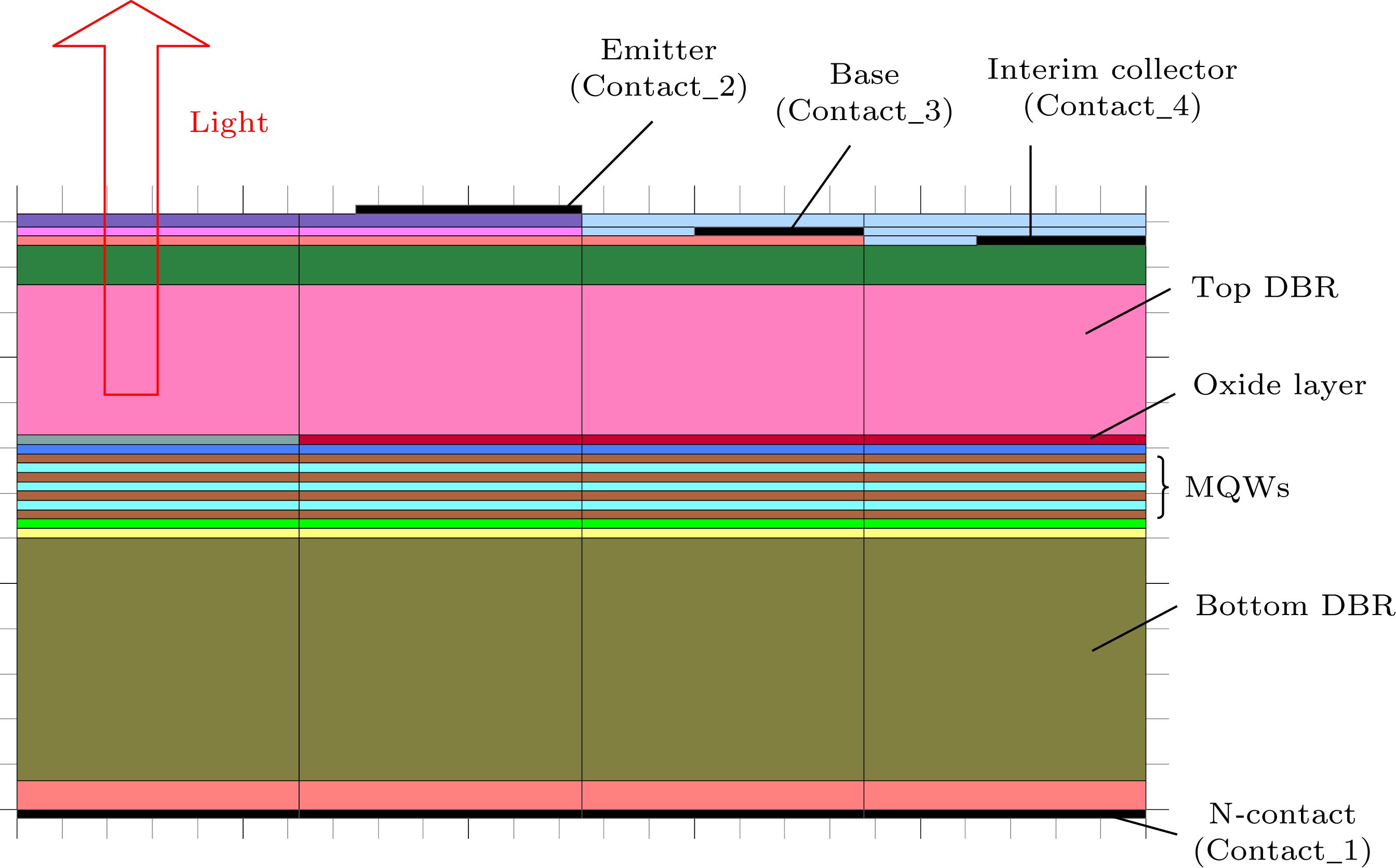
图 1 VCSELs与HBT集成结构示意图
Figure 1. Schematic diagram of integration of VCSELs and HBT.
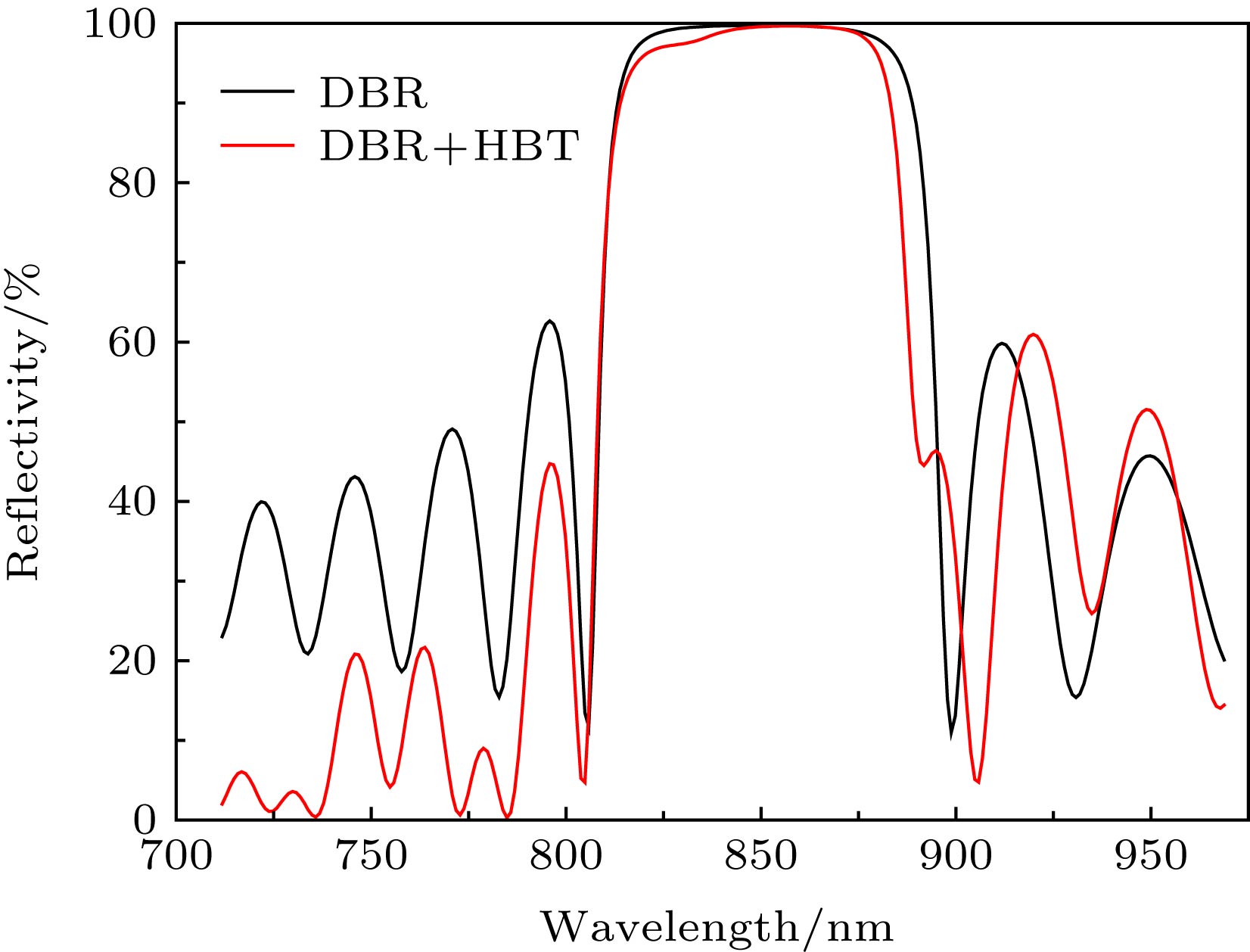
图 2 不同结构DBR反射率
Figure 2. Reflectivity of different DBRs.
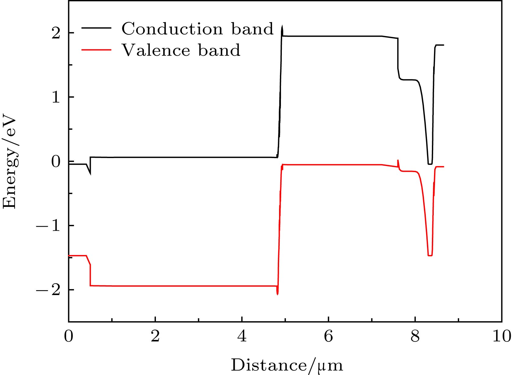
图 3 平衡态时集成结构的能带
Figure 3. Band diagram of integrated structure at equilibrium.
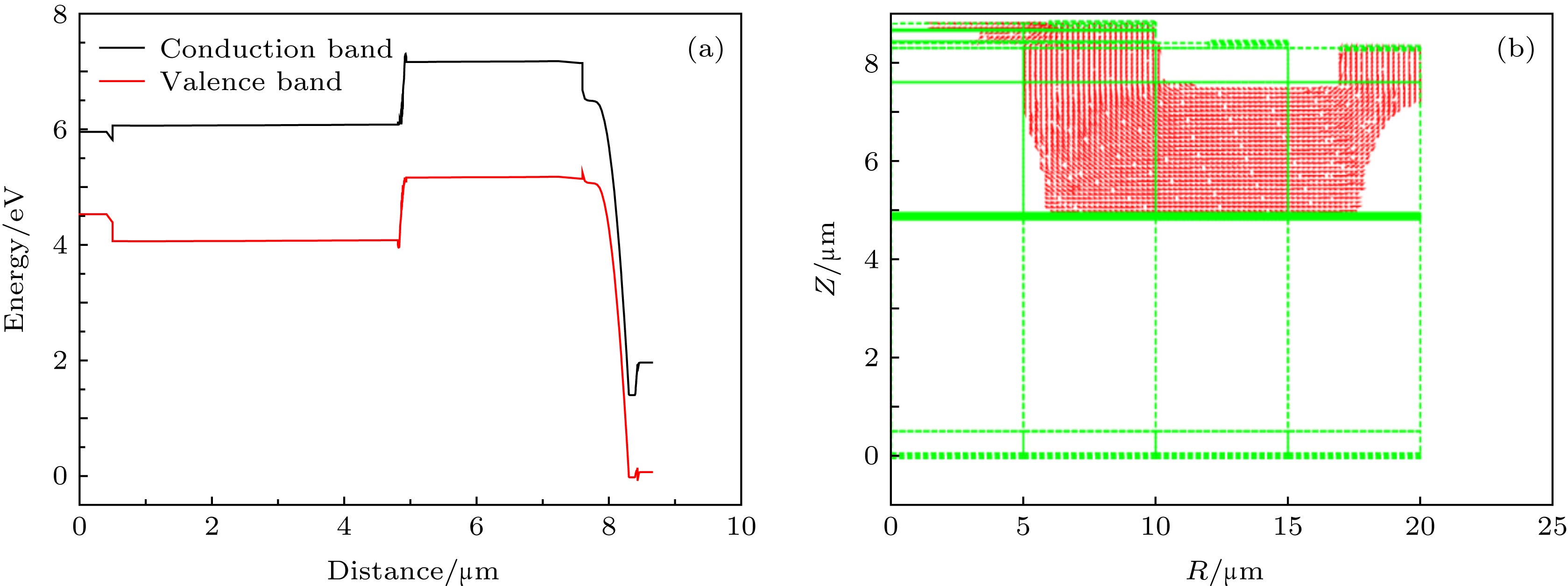
图 4 HBT处于放大状态时的(a)能带图, (b)集成结构内部电流分布
Figure 4. Integrated structure when HBT is in an amplified state: (a) Band diagram; (b) current distribution.
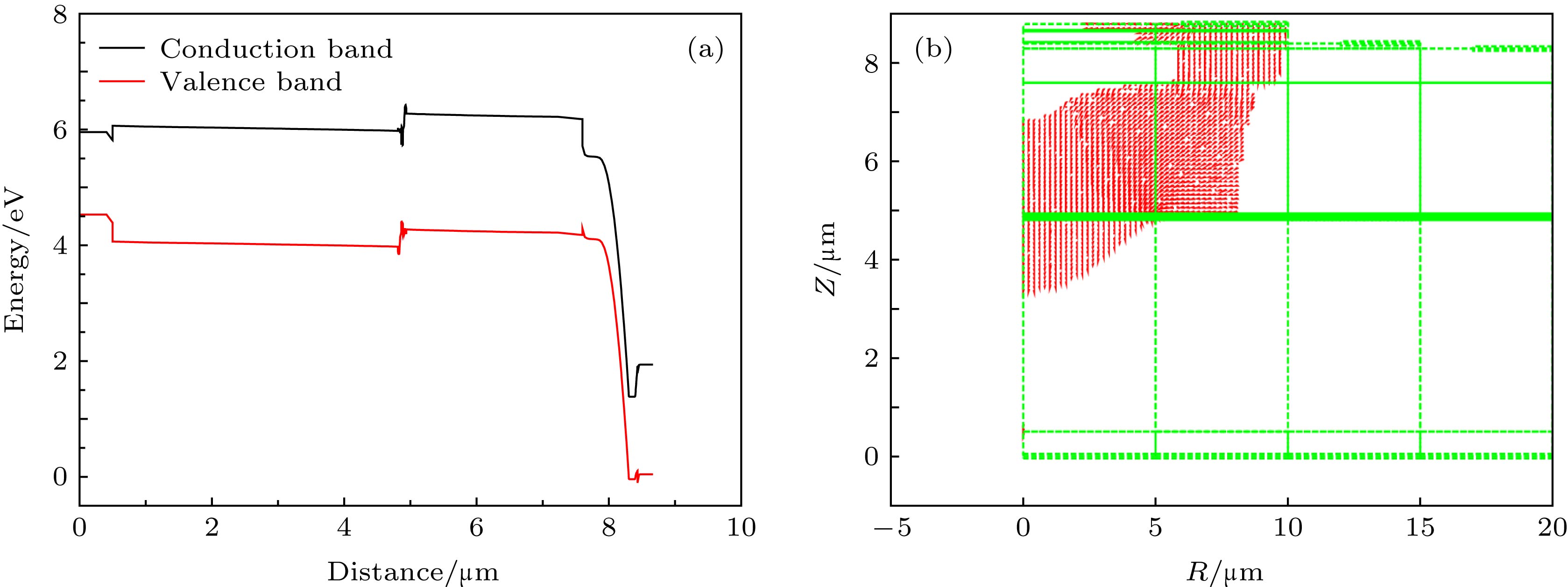
图 5 HBT和VCSEL同时导通时的集成结构 (a)能带图; (b)内部电流分布
Figure 5. Integrated structure when both HBT and VCSELs were conducted: (a) Band diagram; (b) current distribution.
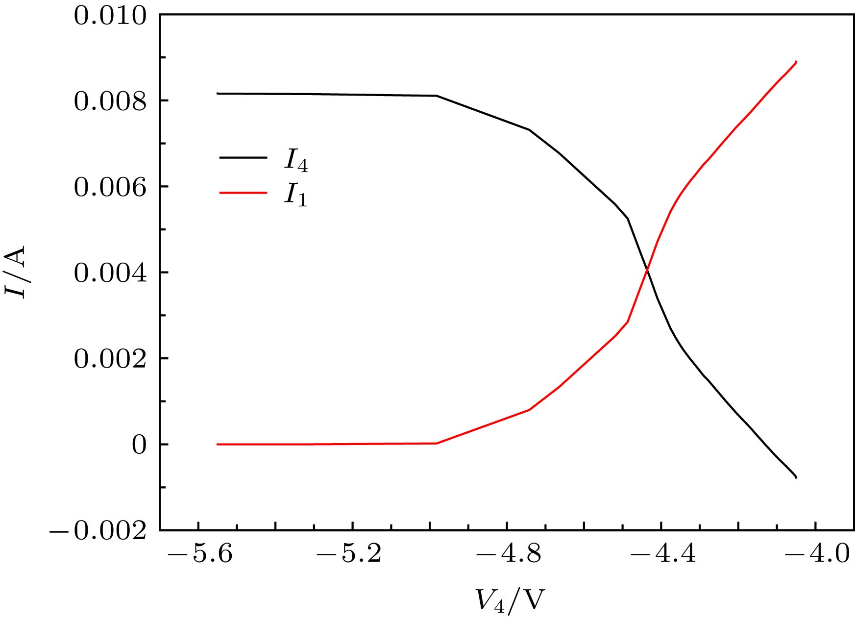
图 6 过渡集电极和N型电极电流随过渡集电极电压的变化
Figure 6. Relations of interim collector currentwith voltage of interim collector.
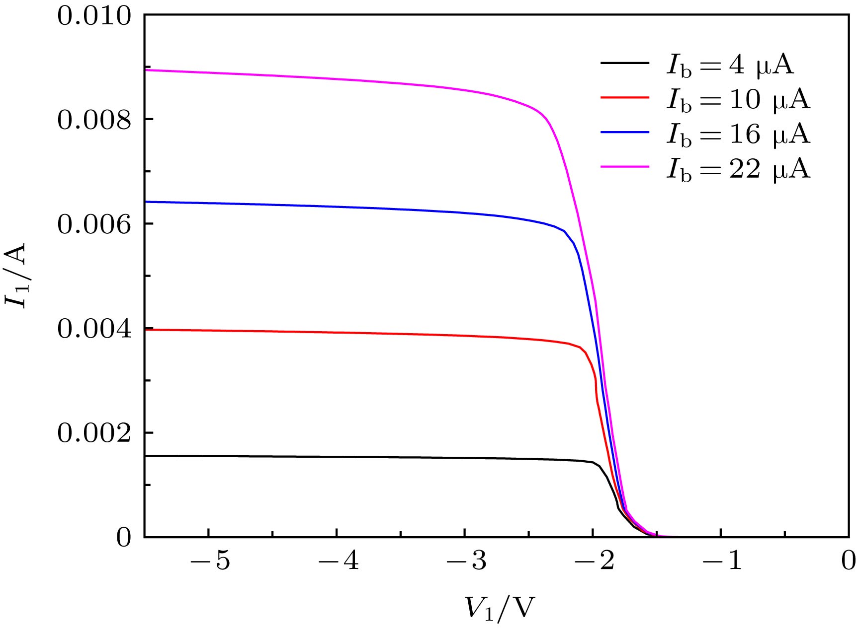
图 7 不同基极电流下N型电极电流随电压的变化
Figure 7. I1 varying with V1 at different base currents.
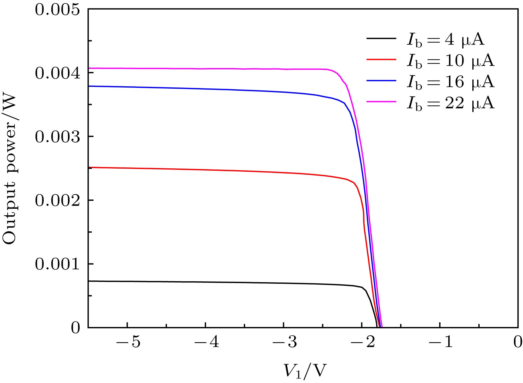
图 8 不同基极电流下输出光功率随N型电极电压的变化
Figure 8. Output power varying with V1 at different base currents.
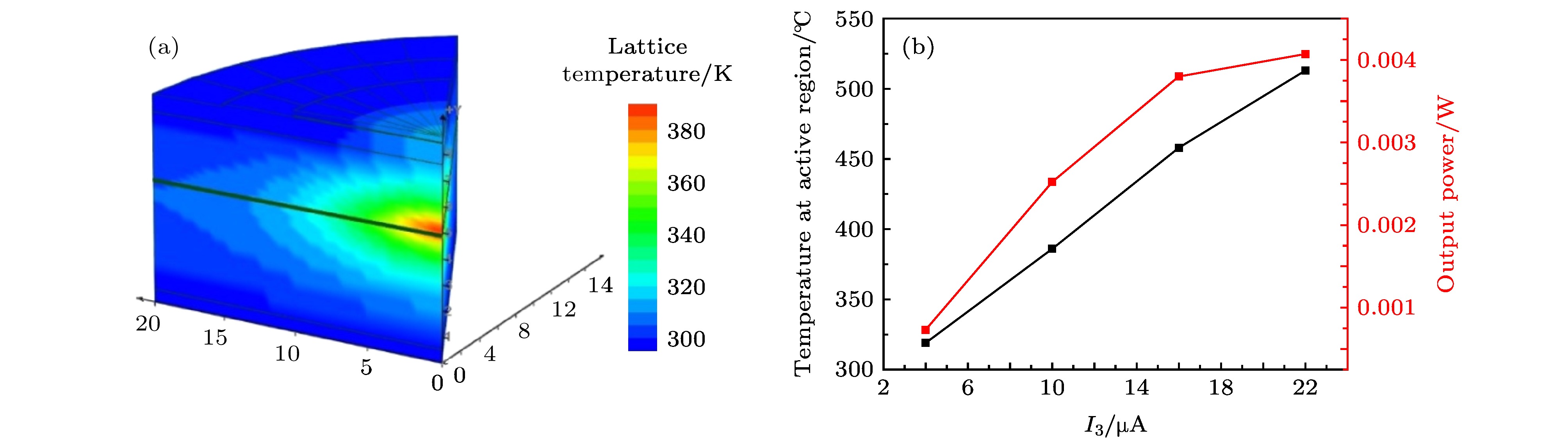
图 9 (a)基极电流为10 μA时器件内部温度分布; (b)有源区温度和输出光功率随基极电流的变化(V1 = –6 V)
Figure 9. (a) Temperature distribution of the device at a 10 μA base current; (b) temperature in active region and output power varying with the base current (V1 = –6 V).
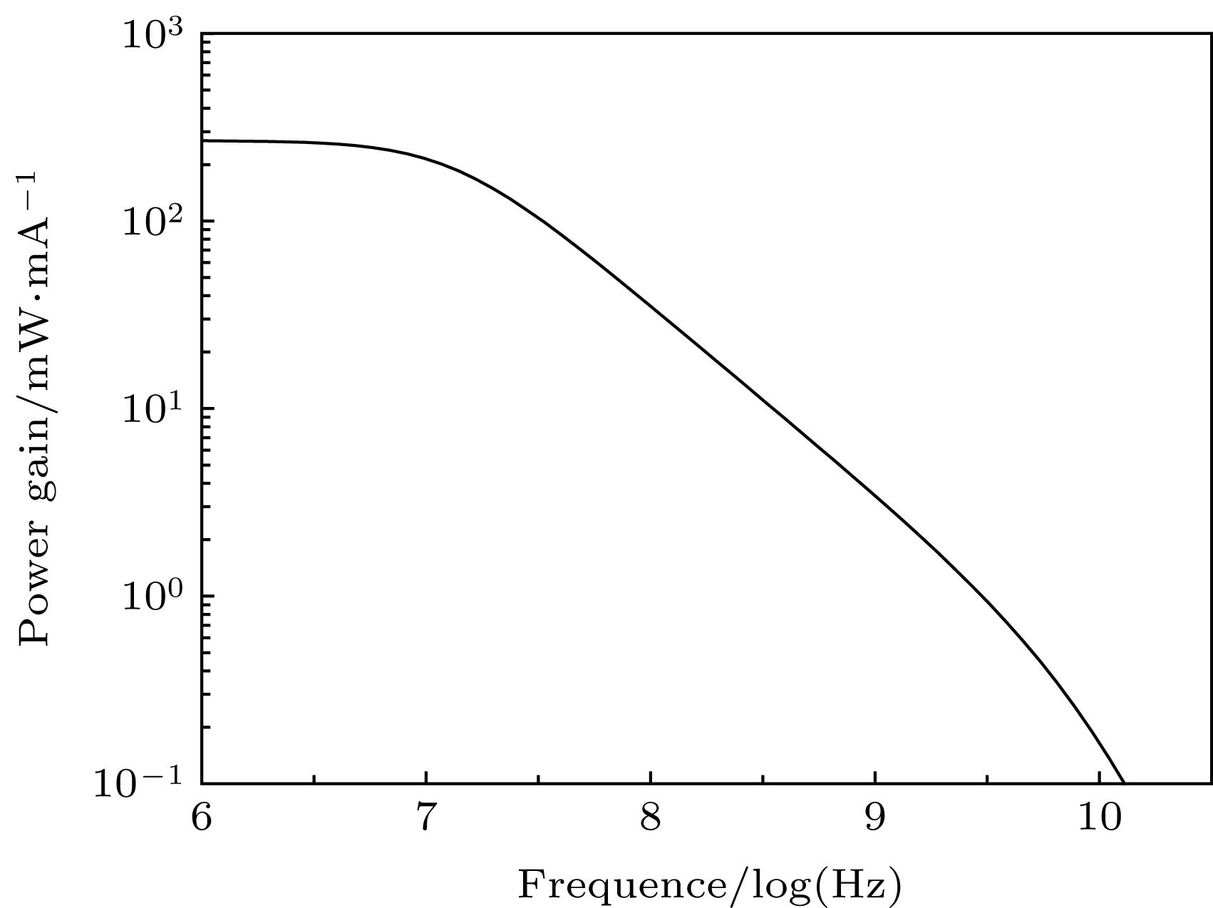
图 10 集成结构的交流光增益
Figure 10. The ac power gain of integration structure.
-
[1] 张星, 张奕, 张建伟, 张建, 钟础宇, 黄佑文, 宁永强, 顾思洪, 王立军 2016 物理学报 65 134204
Google Scholar
Zhang X, Zhang Y, Zhang J W, Zhang J, Zhong C Y, Huang Y W, Ning Y Q, Gu S H, Wang L J 2016 Acta Phys. Sin. 65 134204
Google Scholar
[2] 郝永芹, 冯源, 王菲, 晏长岭, 赵英杰, 王晓华, 王玉霞, 姜会林, 高欣, 薄报学 2011 物理学报 60 064201
Hao Y Q, Feng Y, Wang F, Yan C L, Zhao Y J, Wang X H, Wang Y X, Jiang H L, Gao X, Bao B X 2011 Acta Phys. Sin. 60 064201
[3] 彭红玲, 韩勤, 杨晓红, 牛智川 2006 物理学报 56 863
Peng H L, Han Q, Yang X H, Niu Z C 2006 Acta Phys. Sin. 56 863
[4] 杨威, 刘训春, 朱旻, 王润梅, 申华军 2006 半导体学报 27 1603
Yang W, Liu X C, Zhu M, Wang R M, Shen H J 2006 Chin. J. Semicond. 27 1603
[5] Mishra U K, Singh J 2008 Semiconductor Device Physics and Design (Dordrecht: Springer) p246
[6] Liu X, Yuan J S, Liou J J 2008 Microelectron. Reliab. 48 1212
Google Scholar
[7] Zhou P, Cheng J L, Zolper J C, Lear K L, Chalmers S A, Vawter G A, Leibenguth R E, Adams A C 1993 IEEE Photonic. Tech. L. 5 1035
Google Scholar
[8] Berger P R, Dutta N K, Sivco D L, Cho A Y 1991 Appl. Phys. Lett. 59 2826
Google Scholar
[9] Feng M, Qiu J Y, Holonyak N 2018 IEEE J. Quantum Elect. 54 2000514
[10] Shi W, Faraji B, Greenberg M, Berggren J, Xiang Y, Hammar M, Lestrade M, Li Z Q, Li Z M S, Chrostowski L 2011 Opt. Quant. Electron. 42 659
Google Scholar
[11] Xiang Y, Hedlund C R, Yu X, Yang C, Zabel T, Hammar M, Akram M N 2015 J Opt. Soc. Am. 23 15680
[12] Kuchta D M, Rylyakov A V, Doany F E, Schow C L, Proesel J, Baks C W, Westbergh P, Gustavsson J S, Larsson A 2015 IEEE Photonic Tech. L. 27 577
Google Scholar
[13] Kishi T, Nagatani M, Kanazawa S, Kobayashi W, Nosaka H 2017 J. Lightwave Technol. 35 75
Google Scholar
[14] Rylyakov A V, Larsson A, Baks C W, Schow C L, Kuchta D M, Gustavsson J S, Proesel J E, Westbergh P 2015 J. Lightwave Technol. 33 802
Google Scholar
[15] Han W T, Feng M, Holonyak N, Han W T, Holonyak N 2013 Proc. IEEE 101 2271
Google Scholar
[16] Dems M, Beling P, Gębski M, Piskorski L, Czyszanowski T 2015 Proc. SPIE 9381 98310K-1
[17] Hui L, Jia X 2018 Opt. Commun. 415 1
Google Scholar
[18] Coldren L A, Corzine S W, Milan L M 2012 Diode Lasers and Photonic Integrated Circuits (2nd Ed.) (Hoboken: John Wiley & Sons) p80
[19] Westbergh P, Gustavsson J S, Kögel B, Haglund A, Larsson A 2011 IEEE J. Sel. Top. Quant. 17 1603
Google Scholar
[20] Larisch G, Moser P, Lott J A, Bimberg D 2016 IEEE Photonic Technol. L. 28 2327
Google Scholar

 DownLoad:
Catalog
Metrics
- Abstract views: 7132
- PDF Downloads: 69
- Cited By: 0
