


-
In recent years, α-MoO3 has received extensive attention in the research of memristor devices. The variation of valence of molybdenum will lead the resistivity to change, and the unique layer structure is beneficial to the implantation of donor ion into free space to adjust the conductance, so that it has a great influence on the study of synaptic transistors. This paper mainly summarize the properties of α-MoO3, the method and characteristics of large-scale two-dimensional α-MoO3 and analyze the recent progress of in-memory computing based on α-MoO3. Primarily, this paper introduces crystal structures, band structure and defect state of α-MoO3. The synthesis methods of large-area α-MoO3 are compared with each other, including the one-step method to directly obtain α-MoO3 nanosheets, and the combined post-annealing process of magnetron sputtering or atomic layer deposition to prepare the thin α-MoO3 films. In the one-step synthesis method we conclude that the chamber pressure influences the ratio of MoO3 to MoO3–x, and the growth temperature affects the ratio of α-MoO3 to β-MoO3. That is to say, the phase composition of molybdenum trioxide, the concentration of precursors has an important influence on the film size. The advantages of α-MoO3 synthesis by different methods in memory computing applications are discussed in detail. And then, this paper summarizes the device performance of α-MoO3 in memristor and the application progress of α-MoO3-based neuromorphic devices, and analyzes the performance of α-MoO3-based resistive random access memory such as switching ratio, endurance, and stability in detail. The synaptic functions of different structural device units are extensively studied, and various typical synapse functions are realized such as short-term plasticity, long-term plasticity, paired pulse facilitation, etc. It shows the excellent characteristics of low energy consumption in the simulation of synaptic plasticity. The use of short-term memory and long-term memory modes of the device can realize the functions of image memory and preprocessing. Through the memristor array combined with the back-propagation network, the high-precision handwriting recognition can be realized. Finally, combining the recent research progress of α-MoO3, its opportunities and challenges in the field of memory computing are prospected.
-
Keywords:
- α-MoO3 /
- large-scale synthesis /
- memory computing /
- neuromorphic devices
[1] Yang J J, Strukov D B, Stewart D R 2013 Nat. Nanotechnol. 8 13
 Google Scholar
[2] Chua L O 1971 IEEE Trans. Circuit Theory 18 507
Google Scholar
[3] Ielmini D, Wong H S P 2018 Nat. Electron. 1 333
Google Scholar
[4] Liu Y, Huang Y, Duan X 2019 Nature 567 323
Google Scholar
[5] 张宝军, 王芳, 沈稼强, 单欣, 邸希超, 胡凯, 张楷亮 2020 物理学报 69 048101
Google Scholar
Zhang B J, Wang F, Shen J Q, Shan X, Di X C, Hu K, Zhang K L 2020 Acta Phys. Sin. 69 048101
Google Scholar
[6] Hanson E D, Lajaunie L, Hao S, Myers B D, Shi F, Murthy A A, Wolverton C, Arenal R, Dravid V P 2017 Adv. Funct. Mater. 27 1605380
Google Scholar
[7] Carcia P F, Mccarron E M 1987 Thin Solid Films 155 53
Google Scholar
[8] De Castro I A, Datta R S, Ou J Z, Castellanos-Gomez A, Sriram S, Daeneke T, Kalantar-zadeh K 2017 Adv. Mater. 29 1701619
Google Scholar
[9] Yao D D, Ou J Z, Latham K, Zhuiykov S, O’Mullane A P, Kalantar-zadeh K 2012 Cryst. Growth Des. 12 1865
Google Scholar
[10] Pan W, Tian R, Jin H, Guo Y, Zhang L, Wu X, Zhang L, Han Z, Liu G, Li J, Rao G, Wang H, Chu W 2010 Chem. Mater. 22 6202
Google Scholar
[11] Lei Y H, Chen Z X 2016 Appl. Surf. Sci. 361 107
Google Scholar
[12] Inzani K, Grande T, Vullum-Bruer F, Selbach S M 2016 J. Phys. Chem. C 120 8959
Google Scholar
[13] Wang Y, Du X, Wang J, Su M, Wan X, Meng H, Xie W, Xu J, Liu P 2017 ACS Appl. Mater. Interfaces 9 5543
Google Scholar
[14] Crowley K, Ye G, He R, Abbasi K, Gao X P A 2018 ACS Appl. Nano Mater. 1 6407
Google Scholar
[15] Zhang C, Pudasaini P R, Oyedele A D, Ievlev A V, Xu L, Haglund A V, Noh J H, Wong A T, Xiao K, Ward T Z, Mandrus D G, Xu H, Ovchinnikova O S, Rack P D 2018 ACS Appl. Mater. Interfaces 10 22623
Google Scholar
[16] Zheng B, Wang Z, Chen Y, Zhang W, Li X 2018 2D Mater. 5 045011
Google Scholar
[17] Sun H, Zhang H, Jing X, Hu J, Shen K, Liang Z, Hu J, Tian Q, Luo M, Zhu Z, Jiang Z, Huang H, Song F 2019 Appl. Surf. Sci. 476 789
Google Scholar
[18] Arash A, Ahmed T, Rajan A G, Walia S, Rahman F, Mazumder A, Ramanathan R, Sriram S, Bhaskaran M, Mayes E 2019 2D Mater. 6 035031
Google Scholar
[19] Kim H U, Son J, Kulkarni A, Ahn C, Kim K S, Shin D, Yeom G Y, Kim T 2017 Nanotechnology 28 175601
Google Scholar
[20] Molina-Mendoza A J, Lado J L, Island J O, Niño M A, Aballe L, Foerster M, Bruno F Y, López-Moreno A, Vaquero-Garzon L, van der Zant H S J, Rubio-Bollinger G, Agraït N, Pérez E M, Fernández-Rossier J, Castellanos-Gomez A 2016 Chem. Mater. 28 4042
Google Scholar
[21] Wang D, Li J N, Zhou Y, Xu D H, Xiong X, Peng R W, Wang M 2016 Appl. Phys. Lett. 108 053107
Google Scholar
[22] Diaz-Droguett D E, Fuenzalida V M 2010 J. Nanosci. Nanotechnol. 10 6694
Google Scholar
[23] Cauduro A L F, dos Reis R, Chen G, Schmid A K, Méthivier C, Rubahn H G, Bossard-Giannesini L, Cruguel H, Witkowski N, Madsen M 2017 ACS Appl. Mater. Interfaces 9 7717
Google Scholar
[24] Arita M, Kaji H, Fujii T, Takahashi Y 2012 Thin Solid Films 520 4762
Google Scholar
[25] George S M 2010 Chem. Rev. 110 111
Google Scholar
[26] Leskelä M , Ritala M 2002 Thin Solid Films 1 138
Google Scholar
[27] Shi M L, Chen L, Zhang T B, Xu J, Zhu H, Sun Q Q, Zhang D W 2017 Small 13 1603157
Google Scholar
[28] Diskus M, Nilsen O, Fjellvåg H 2011 J. Mater. Chem. 21 705
Google Scholar
[29] Diskus M, Nilsen O, Fjellvåg H, et al. 2012 J. Vac. Sci. Technol. 30 01A107
Google Scholar
[30] Zhou G, Ren Z, Wang L, Sun B, Duan S, Song Q 2019 Mater. Horiz. 6 1877
Google Scholar
[31] Zhou G, Wu J, Wang L, et al. 2019 Nanoscale 11 17222
Google Scholar
[32] Sun L, Zhang Y, Han G, Hwang G, Jiang J, Joo B, Watanabe K, Taniguchi T, Kim Y M, Yu W J, Kong B S, Zhao R, Yang H 2019 Nat. Commun. 10 3161
Google Scholar
[33] 张志超, 王芳, 吴仕剑, 李毅, 弥伟, 赵金石, 张楷亮 2018 物理学报 67 057301
Google Scholar
Zhang Z C, Wang F, Wu S J, Li Y, Mi W, Zhao J S, Zhang K L 2018 Acta Phys. Sin. 67 057301
Google Scholar
[34] Du H, Chen J, Tu M, Luo S, Li S, Yuan S, Gong T, Huang W, Jie W, Hao J 2019 J. Mater. Chem. C 7 12160
Google Scholar
[35] Zhou F, Zhou Z, Chen J, Choy T H, Wang J, Zhang N, Lin Z, Yu S, Kang J, Wong H S P, Chai Y 2019 Nat. Nanotechnol. 14 776
Google Scholar
[36] Tan Z H, Yin X B, Guo X 2015 Appl. Phys. Lett. 106 023503
Google Scholar
[37] Wang J, Wang F, Yin L, Sendeku M G, Zhang Y, Cheng R, Wang Z, Li N, Huang W, He J 2019 Nanoscale 11 20497
Google Scholar
[38] Rahman F, Ahmed T, Walia S, Mayes E, Sriram S, Bhaskaran M, Balendhran S 2018 Nanoscale 10 19711
Google Scholar
[39] Yang C S, Shang D S, Chai Y S, Yan L Q, Shen B G, Sun Y 2016 Phys. Chem. Chem. Phys. 18 12466
Google Scholar
[40] Hasegawa J, Nagase T, Kobayashi T, Naito H 2016 Jpn. J. Appl. Phys. 55 03DC05
Google Scholar
[41] Abhijith T, Kumar T V, Reddy V S 2017 Nanotechnology 28 095203
Google Scholar
[42] Hsu C C, Wang S Y, Lin Y S, Chen Y T 2019 J. Alloys Compd. 779 609
Google Scholar
[43] Fang S L, Liu W H, Li X, Wang X L, Geng L, Wu M S, Huang X D, Han C Y 2019 Appl. Phys. Lett. 115 244102
Google Scholar
[44] Dai T, Qian L, Ren Y, Liu X 2017 International Conference on Electron Devices and Solid-State Circuits (EDSSC) Hsinchu, Taiwan China, October 18–20, 2017 p1
[45] Xue Q, Wang Y C, Wei X H 2019 Appl. Surf. Sci. 479 469
Google Scholar
[46] Kim G H, Lee, J H, Ahn Y, Jeon W, Song S J, Seok J Y, Yoon J H, Yoon K J, Park T J, Hwang C S 2013 Adv. Funct. Mater. 23 1440
Google Scholar
[47] Rehman M M, Rehman H M M U, Gul J Z, Kim W Y, Karimov K S, Ahmed N 2020 Sci. Technol. Adv. Mater. 21 147
Google Scholar
[48] Wang X, Xie W, Xu J B 2014 Adv. Mater. 26 5496
Google Scholar
[49] Yang C S, Shang D S, Chai Y S, Yan L Q, Shen B G, Sun Y 2017 Phys. Chem. Chem. Phys. 19 4190
Google Scholar
[50] Wang Z, Yang R, Huang H M, He H K, Shaibo J, Guo X 2020 Adv. Electron. Mater. 6 1901290
Google Scholar
[51] Danesh C D, Shaffer C M, Nathan D, Shenoy R, Tudor A, Tadayon M, Lin Y, Chen Y 2019 Adv. Mater. 31 e1808032
Google Scholar
[52] Lenz J, Del Giudice F, Geisenhof F R, Winterer F, Weitz R T 2019 Nat. Nanotechnol. 14 579
Google Scholar
[53] Nie S, He Y, Liu R, Shi Y, Wan Q 2019 IEEE Electron Device Lett. 40 459
Google Scholar
[54] Chernova N A, Roppolo M, Dillon A C, Whittingham M S 2009 J. Mater. Chem. 19 2526
Google Scholar
[55] 李琦, 章勇 2018 物理学报 67 067201
Google Scholar
Li Q, Zhang Y 2018 Acta Phys. Sin. 67 067201
Google Scholar
[56] Yang C S, Shang D S, Liu N, Shi G, Shen X, Yu R C, Li Y Q, Sun Y 2017 Adv. Mater. 29 1700906
Google Scholar
[57] Yang C S, Shang D S, Liu N, et al. 2018 Adv. Funct. Mater. 28 1804170
Google Scholar
[58] He Y, Nie S, Liu R, Jiang S, Shi Y, Wan Q 2019 Adv. Mater. 31 e1900903
Google Scholar
[59] Guo L, Wen J, Ding J, Wan C, Cheng G 2016 Sci. Rep. 6 38578
Google Scholar
[60] Hu W, Jiang J, Xie D, Liu B, Yang J, He J 2019 J. Mater. Chem. C 7 682
Google Scholar
[61] Shao L, Wang H, Yang Y, et al. 2019 ACS Appl. Mater. Interfaces 11 12161
Google Scholar
[62] Wang K, Dai S, Zhao Y, Wang Y, Liu C, Huang J 2019 Small 15 e1900010
Google Scholar
-

图 1 (a) α-MoO3晶体结构; (b) β-MoO3晶体结构; (c) h-MoO3晶体结构
Figure 1. (a) Crystal structure of α-MoO3; (b) crystal structure of β-MoO3; (c) crystal structure of h-MoO3.
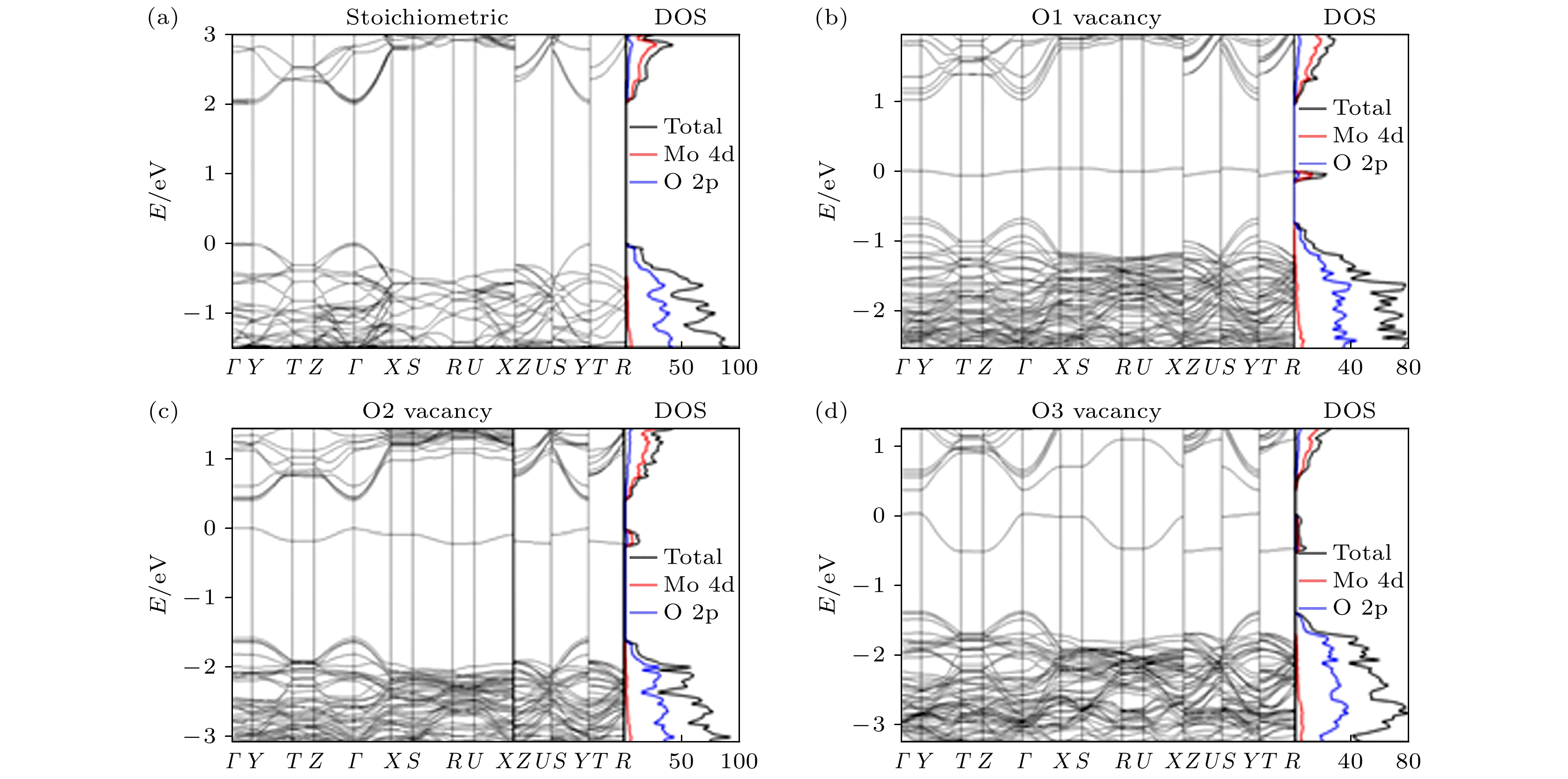
图 3 (a) 在化学计量比情况下MoO3能带结构[12]; (b) 在O1空位情况下MoO3能带结构[12]; (c) 在O2 空位情况下MoO3能带结构[12]; (d) 在O3空位情况下MoO3能带结构[12]
Figure 3. (a) Band structures of MoO3 in the stoichiometric case[12]; (b) band structures of MoO3 in the vacancy on O1 case[12]; (c) band structures of MoO3 in the vacancy on O2 case[12]; (d) band structures of MoO3 in the vacancy on O3 case[12].
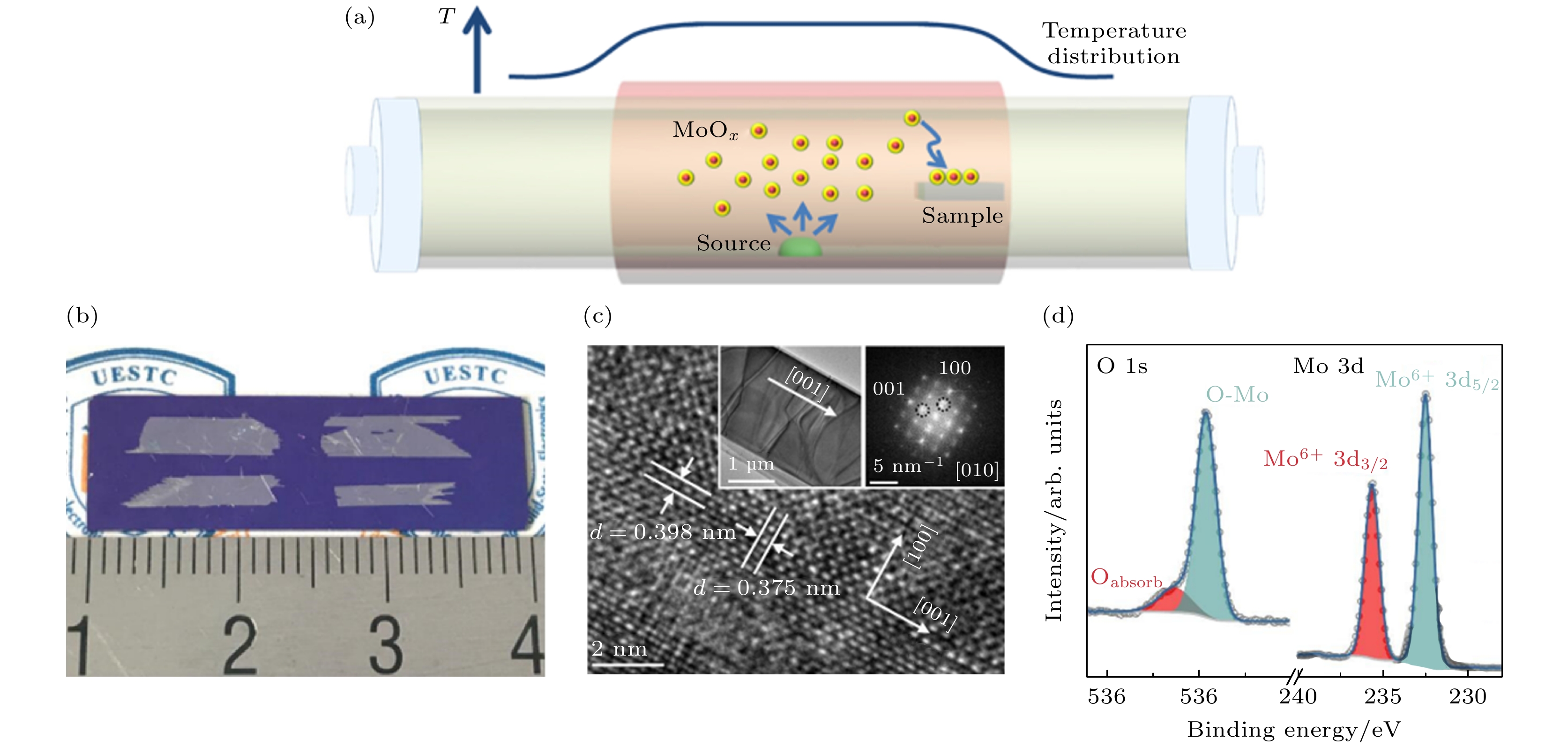
图 4 (a) 在两温区的物理气相沉积系统中合成α-MoO3原理图[13]; (b) 在SiO2/Si衬底上生长的α-MoO3单晶的照片[16]; (c) α-MoO3的HRTEM图像, 内嵌图为相应的透射电子显微镜图像和傅里叶变换图像[16]; (d) 生长α-MoO3的O 1s和Mo 3d的高分辨XPS能谱[16]
Figure 4. (a) Schematic illustration of synthesis of α-MoO3 in a two-temperature-zone PVD system[13]; (b) photograph of as-grown α-MoO3 single crystals on SiO2/Si substrate[16]; (c) HRTEM image of the α-MoO3 sheet. Insets: corresponding TEM and FFT images[16]; (d) high-resolution XPS spectra of O 1s and Mo 3d of as-grown α-MoO3[16].
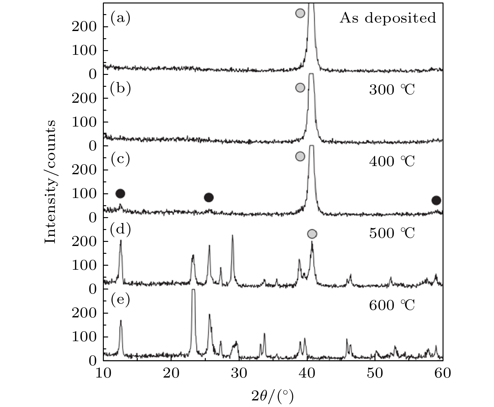
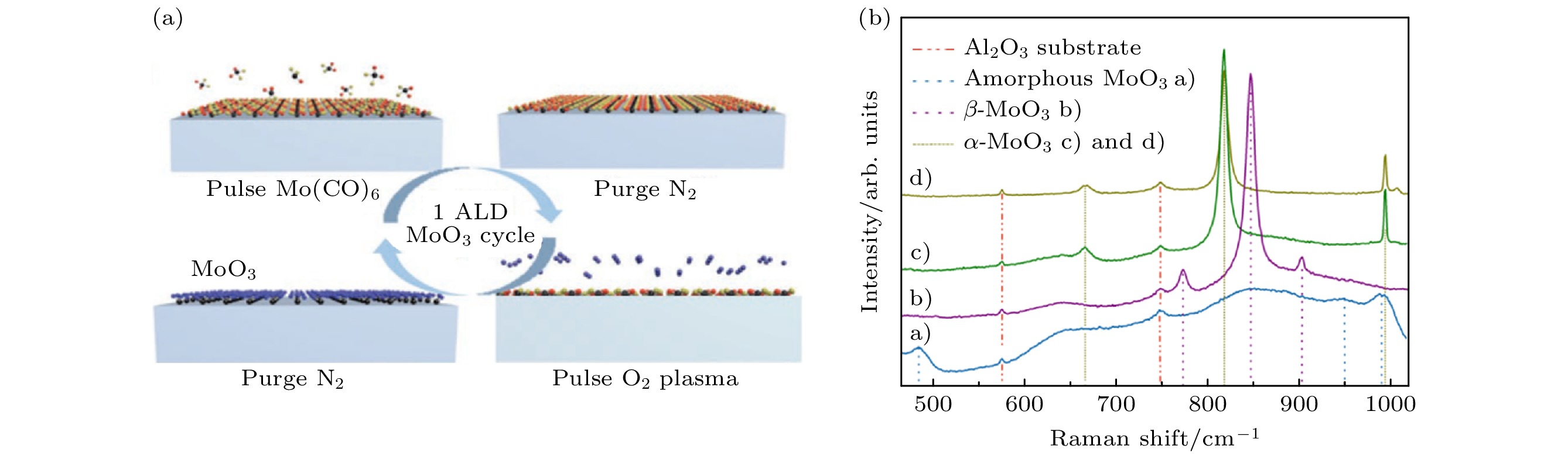
图 6 (a) 采用ALD合成MoO3薄膜的一个循环的工艺原理图[27]; (b) 采用ALD在Al2O3上沉积得到的40 nm MoO3薄膜的拉曼光谱: a)沉积和空气中退火, b) 400 ℃退火8 min, c) 600 ℃退火4 min, d) 600 ℃退火7.5 min[29]
Figure 6. (a) Schematic of one cycle ALD process for MoO3 film[27]; (b) Raman spectra of 40 nm thin films of MoO3 deposited on Al2O3 by ALD: a) as deposited, and annealed in air; b) 8 min at 400 ℃; c) 4 min at 600 ℃; d) 7.5 min at 600 ℃[29].
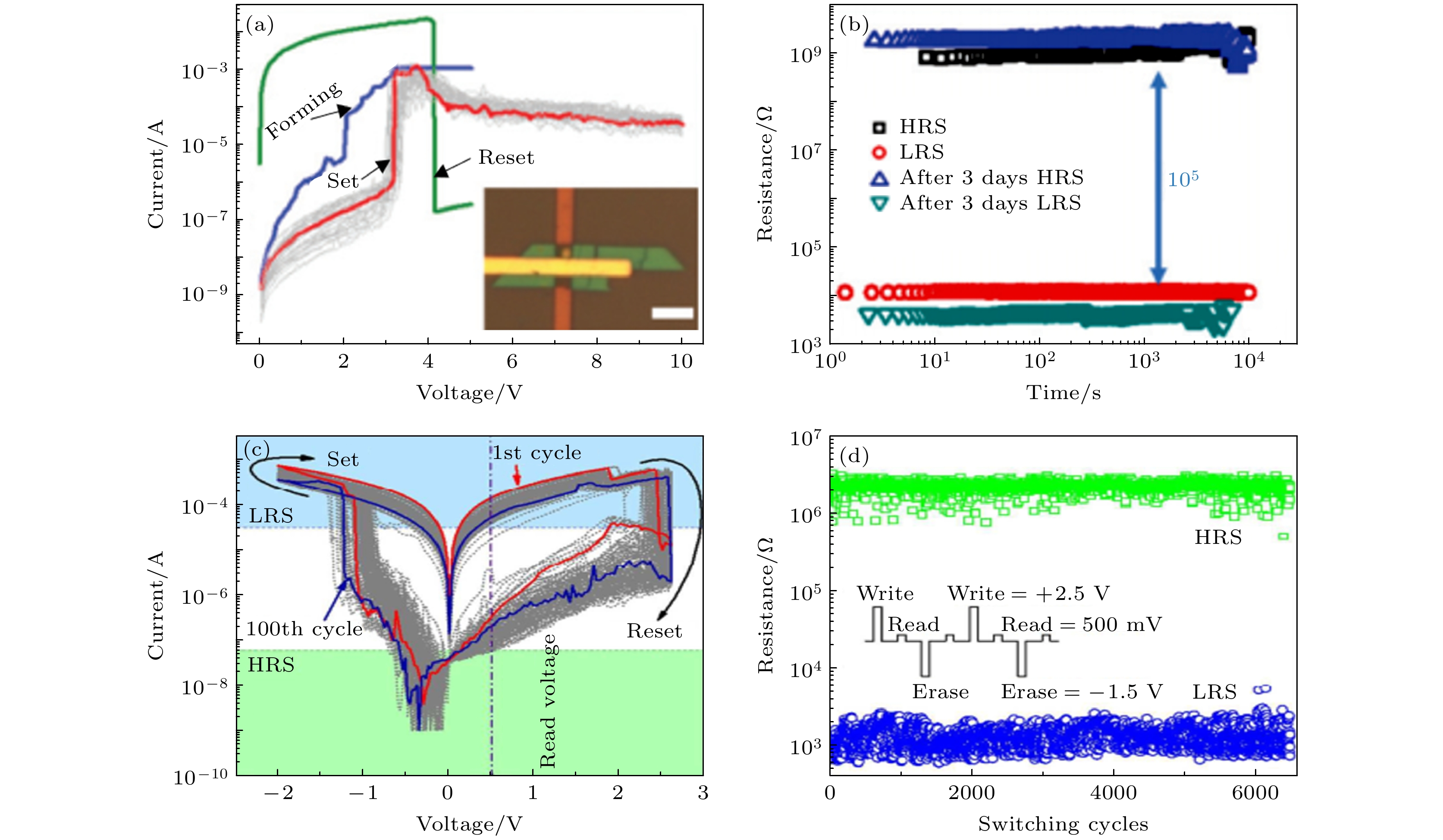
图 7 (a) 单极电阻开关的代表性行为, 横向面积为2 μm × 2 μm的α-MoO3横杆三明治器件中的I-V曲线, 内嵌图显示了Au/Cr/α-MoO3/Au横杆夹层结构的相应光学图像, 刻度线代表5 μm[37]; (b) α-MoO3横杆器件开关在室温下具有稳定的保持性; 在0.01 V的小偏置下, 通过测量电流来确定HRS和LRS[37]; (c) 存储器单元在重复开关周期下的特性电流-电压曲线[38]; (d) 开关周期的耐久性(读取电压为500 mV时获得的电阻值), 内嵌图为耐久性测量过程中的电压脉冲序列, 每个脉冲的持续时间为2 ms[38]
Figure 7. (a) Representative I-V curves of unipolar resistive switching behavior in the α-MoO3 crossbar sandwich device with a lateral area of 2 μm × 2 μm. The inset shows the corresponding optical image of Au/Cr/α-MoO3/Au crossbar sandwich structures and the scale bar represents 5 μm[37]. (b) Time-dependent measurements of α-MoO3 crossbar device switch featuring stable retention at room temperature. The resistance of the HRS and LRS is determined by measuring the current at a small bias of 0.01 V[37]. (c) Characteristic current-voltage curves of a memory cell subjected to repetitive switching cycles[38]. (d) Performance endurance with respect to number of switching cycles (Resistance values obtained at a read voltage of 500 mV). The inset shows the voltage pulse train during endurance measurement with duration of 2 ms of each pulse[38].
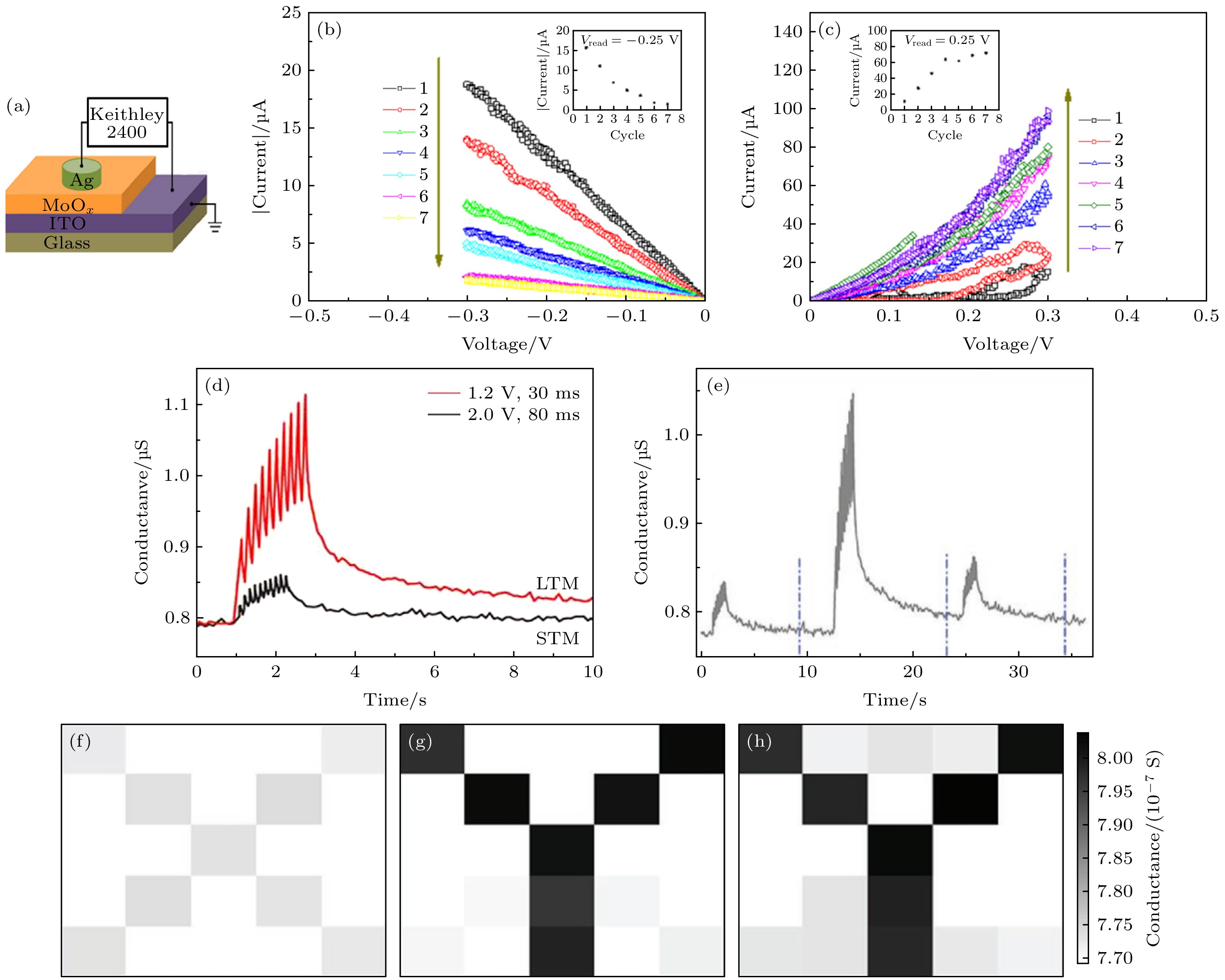
图 9 (a) 垂直器件结构示意图及测试说明[45]; (b) 负电压I-V曲线[45]; (c) 正电压I-V曲线; 内嵌图为 ± 0.25 V读电压下随周期的增加, 电流的变化[45]; (d) 由施加的10个不同电压和宽度的脉冲所表示的STM和LTM[50]; (e) 电导在第一个像素内的变化, 蓝色虚线表示对于一个给定字母, 输入最后一个脉冲后的读出时间[50]; (f), (g), (h)在STM模式下(e)图中蓝线标记的时刻所记忆的字母“x”和“z”, 而字母“y”是在LTM模式下被记忆[50]
Figure 9. (a) Schematic illustration of vertical device structure and measurement; (b) I-V curves of negative voltage[45]; (c) I-V curves of positive voltage, the insets show the variation of the current read at ±0.25 V with increasing cycle[45]; (d) STM and LTM demonstrated by applying 10 pulses with different amplitudes and widths[50]; (e) conductance change at the first pixel; the blue dashed lines indicate the read-out moment after inputting the last pulse for a given letter[50]; (f), (g), (h) images memorized at the moments marked by blue lines in (e) letters “x” and “z” are memorized in the STM mode, while the letter “y” is memorized in the LTM mode[50].
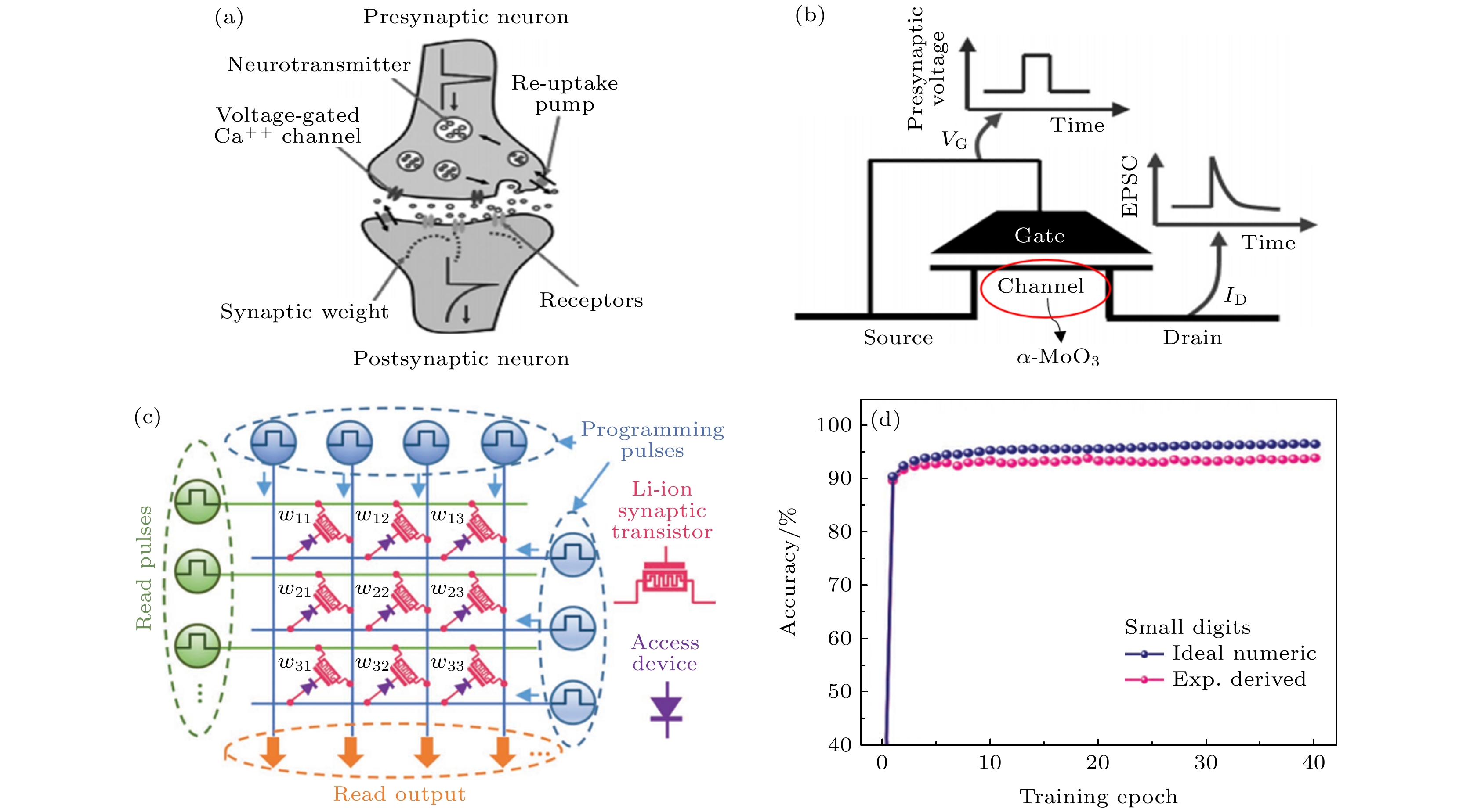
图 10 (a) 生物突触示意图[56]; (b) 三端突触晶体管结构原理图[56]; (c) 由电压编程锂离子突触晶体管crossbar阵列和接入器件组成的突触权重层示意图[57]; (d) 对于8 × 8像素手写数字图像, 其识别精度随训练epochs的变化[57]
Figure 10. (a) Schematic illustration of a biological synapse[56]; (b) schematic diagram of the three-terminal synaptic transistor[56]; (c) schematics of a synaptic weight layer composed of voltage programmed Li-ion synaptic transistor crossbar array and access devices[57]; (d) the recognition accuracy evolution with training epochs for 8 × 8 pixel handwritten digit image[57].
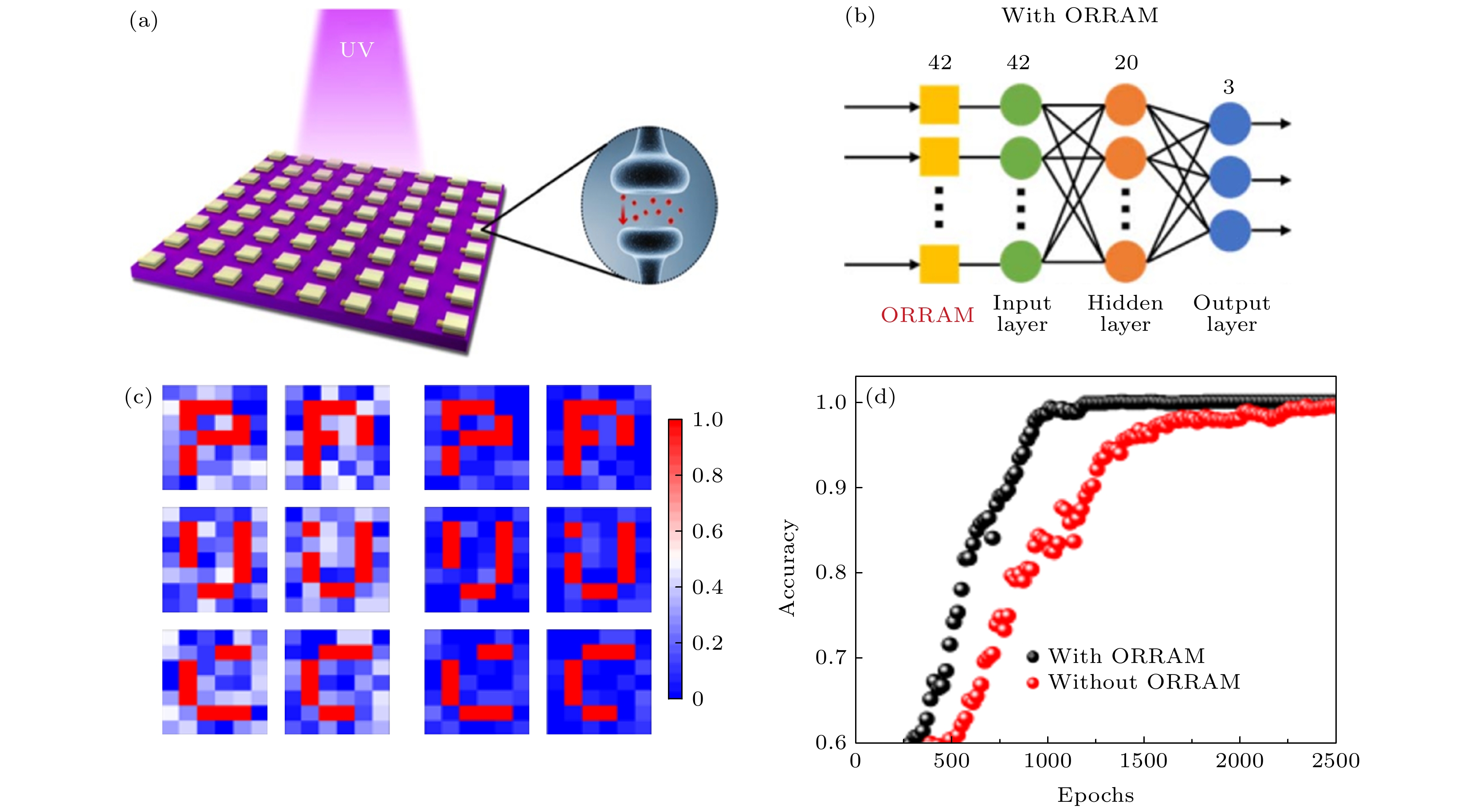
图 11 (a) 8 × 8 ORRAM阵列原理图[35]; (b) 带有ORRAM阵列的三层人工神经网络连接结构[35]; (c) 经ORRAM阵列预处理前(左列)和后(右列)的图像示例[35]; (d) 有无ORRAM阵列图像预处理情况下图像识别率的对比[35]
Figure 11. (a) Schematic structure of an 8 × 8 ORRAM array[35]; (b) structure of the three-layered artificial neural network with ORRAM[35]; (c) examples of images before (left columns) and after (right columns) ORRAM-based pre-processing[35]; (d) comparisons of the image recognition rate with and without ORRAM-based image preprocessing[35].
表 1 一步法制备α-MoO3的生长条件(1 Torr = 1.33322 × 10² Pa)
Table 1. Growth conditions of α-MoO3 prepared by one-step method.
Ref. Carrier flow Pressure Substrate temperature/℃ Growth time/min Lateral size Thickness/nm [13] — Atmospheric 580 120 69.6 μm 5.3—89.8 [16] — Atmospheric 850—1050 30 0.72 cm — [17] Ar Atmospheric 750 20 Centimeters scale 4.3—550 [18] Ar 310 mTorr 530 45 500 µm × 500 µm 8 ± 0.75 [19] Ar & O2 100 mTorr 150 90 Wafer-scale 30 [20] — Atmospheric 540 20 Centimeters scale ≥ 1.4 [21] N2 Atmospheric 350—480 20 Several tens micron 2.8—14  DownLoad: CSV
表 2 三氧化钼基忆阻器件性能对比
Table 2. Comparison of performance of molybdenum trioxide memristors.
Ref. Ron/Roff Endurence Vforming/V Vset/V Vreset/V Retention/s Compliance/mA [24] 10—102 60 1.8—3 1—2 0.5—1 — 2—5 [36] 103 — –2.2 1.7 3.3 103 10-3 [37] > 105 50 3.2—4.1 3—3.9 4.45—5.9 104 50 [38] 103 > 6000 –2.7 –2 2.5 > 104 0.8 [39] 18 — 24.5 1.8 –1.1 3.6 × 10³ 1 [40] ~350 — — 1—3 — 2.6 × 10⁶ — [41] 1.15 × 10³ 7 — 4 8 4.5 × 10³ — [42] 1.6 × 10² 500 — –3 3 — — [43] 106 > 100 — 0.8 –0.2—1.6 2 × 10⁴ 102 [44] 20 — — 2.2 –1.1 1.4 × 10³ 0.1 [45] — — Free 0.4 –1 — 0.1
DownLoad: CSV
-
[1] Yang J J, Strukov D B, Stewart D R 2013 Nat. Nanotechnol. 8 13
Google Scholar
[2] Chua L O 1971 IEEE Trans. Circuit Theory 18 507
Google Scholar
[3] Ielmini D, Wong H S P 2018 Nat. Electron. 1 333
Google Scholar
[4] Liu Y, Huang Y, Duan X 2019 Nature 567 323
Google Scholar
[5] 张宝军, 王芳, 沈稼强, 单欣, 邸希超, 胡凯, 张楷亮 2020 物理学报 69 048101
Google Scholar
Zhang B J, Wang F, Shen J Q, Shan X, Di X C, Hu K, Zhang K L 2020 Acta Phys. Sin. 69 048101
Google Scholar
[6] Hanson E D, Lajaunie L, Hao S, Myers B D, Shi F, Murthy A A, Wolverton C, Arenal R, Dravid V P 2017 Adv. Funct. Mater. 27 1605380
Google Scholar
[7] Carcia P F, Mccarron E M 1987 Thin Solid Films 155 53
Google Scholar
[8] De Castro I A, Datta R S, Ou J Z, Castellanos-Gomez A, Sriram S, Daeneke T, Kalantar-zadeh K 2017 Adv. Mater. 29 1701619
Google Scholar
[9] Yao D D, Ou J Z, Latham K, Zhuiykov S, O’Mullane A P, Kalantar-zadeh K 2012 Cryst. Growth Des. 12 1865
Google Scholar
[10] Pan W, Tian R, Jin H, Guo Y, Zhang L, Wu X, Zhang L, Han Z, Liu G, Li J, Rao G, Wang H, Chu W 2010 Chem. Mater. 22 6202
Google Scholar
[11] Lei Y H, Chen Z X 2016 Appl. Surf. Sci. 361 107
Google Scholar
[12] Inzani K, Grande T, Vullum-Bruer F, Selbach S M 2016 J. Phys. Chem. C 120 8959
Google Scholar
[13] Wang Y, Du X, Wang J, Su M, Wan X, Meng H, Xie W, Xu J, Liu P 2017 ACS Appl. Mater. Interfaces 9 5543
Google Scholar
[14] Crowley K, Ye G, He R, Abbasi K, Gao X P A 2018 ACS Appl. Nano Mater. 1 6407
Google Scholar
[15] Zhang C, Pudasaini P R, Oyedele A D, Ievlev A V, Xu L, Haglund A V, Noh J H, Wong A T, Xiao K, Ward T Z, Mandrus D G, Xu H, Ovchinnikova O S, Rack P D 2018 ACS Appl. Mater. Interfaces 10 22623
Google Scholar
[16] Zheng B, Wang Z, Chen Y, Zhang W, Li X 2018 2D Mater. 5 045011
Google Scholar
[17] Sun H, Zhang H, Jing X, Hu J, Shen K, Liang Z, Hu J, Tian Q, Luo M, Zhu Z, Jiang Z, Huang H, Song F 2019 Appl. Surf. Sci. 476 789
Google Scholar
[18] Arash A, Ahmed T, Rajan A G, Walia S, Rahman F, Mazumder A, Ramanathan R, Sriram S, Bhaskaran M, Mayes E 2019 2D Mater. 6 035031
Google Scholar
[19] Kim H U, Son J, Kulkarni A, Ahn C, Kim K S, Shin D, Yeom G Y, Kim T 2017 Nanotechnology 28 175601
Google Scholar
[20] Molina-Mendoza A J, Lado J L, Island J O, Niño M A, Aballe L, Foerster M, Bruno F Y, López-Moreno A, Vaquero-Garzon L, van der Zant H S J, Rubio-Bollinger G, Agraït N, Pérez E M, Fernández-Rossier J, Castellanos-Gomez A 2016 Chem. Mater. 28 4042
Google Scholar
[21] Wang D, Li J N, Zhou Y, Xu D H, Xiong X, Peng R W, Wang M 2016 Appl. Phys. Lett. 108 053107
Google Scholar
[22] Diaz-Droguett D E, Fuenzalida V M 2010 J. Nanosci. Nanotechnol. 10 6694
Google Scholar
[23] Cauduro A L F, dos Reis R, Chen G, Schmid A K, Méthivier C, Rubahn H G, Bossard-Giannesini L, Cruguel H, Witkowski N, Madsen M 2017 ACS Appl. Mater. Interfaces 9 7717
Google Scholar
[24] Arita M, Kaji H, Fujii T, Takahashi Y 2012 Thin Solid Films 520 4762
Google Scholar
[25] George S M 2010 Chem. Rev. 110 111
Google Scholar
[26] Leskelä M , Ritala M 2002 Thin Solid Films 1 138
Google Scholar
[27] Shi M L, Chen L, Zhang T B, Xu J, Zhu H, Sun Q Q, Zhang D W 2017 Small 13 1603157
Google Scholar
[28] Diskus M, Nilsen O, Fjellvåg H 2011 J. Mater. Chem. 21 705
Google Scholar
[29] Diskus M, Nilsen O, Fjellvåg H, et al. 2012 J. Vac. Sci. Technol. 30 01A107
Google Scholar
[30] Zhou G, Ren Z, Wang L, Sun B, Duan S, Song Q 2019 Mater. Horiz. 6 1877
Google Scholar
[31] Zhou G, Wu J, Wang L, et al. 2019 Nanoscale 11 17222
Google Scholar
[32] Sun L, Zhang Y, Han G, Hwang G, Jiang J, Joo B, Watanabe K, Taniguchi T, Kim Y M, Yu W J, Kong B S, Zhao R, Yang H 2019 Nat. Commun. 10 3161
Google Scholar
[33] 张志超, 王芳, 吴仕剑, 李毅, 弥伟, 赵金石, 张楷亮 2018 物理学报 67 057301
Google Scholar
Zhang Z C, Wang F, Wu S J, Li Y, Mi W, Zhao J S, Zhang K L 2018 Acta Phys. Sin. 67 057301
Google Scholar
[34] Du H, Chen J, Tu M, Luo S, Li S, Yuan S, Gong T, Huang W, Jie W, Hao J 2019 J. Mater. Chem. C 7 12160
Google Scholar
[35] Zhou F, Zhou Z, Chen J, Choy T H, Wang J, Zhang N, Lin Z, Yu S, Kang J, Wong H S P, Chai Y 2019 Nat. Nanotechnol. 14 776
Google Scholar
[36] Tan Z H, Yin X B, Guo X 2015 Appl. Phys. Lett. 106 023503
Google Scholar
[37] Wang J, Wang F, Yin L, Sendeku M G, Zhang Y, Cheng R, Wang Z, Li N, Huang W, He J 2019 Nanoscale 11 20497
Google Scholar
[38] Rahman F, Ahmed T, Walia S, Mayes E, Sriram S, Bhaskaran M, Balendhran S 2018 Nanoscale 10 19711
Google Scholar
[39] Yang C S, Shang D S, Chai Y S, Yan L Q, Shen B G, Sun Y 2016 Phys. Chem. Chem. Phys. 18 12466
Google Scholar
[40] Hasegawa J, Nagase T, Kobayashi T, Naito H 2016 Jpn. J. Appl. Phys. 55 03DC05
Google Scholar
[41] Abhijith T, Kumar T V, Reddy V S 2017 Nanotechnology 28 095203
Google Scholar
[42] Hsu C C, Wang S Y, Lin Y S, Chen Y T 2019 J. Alloys Compd. 779 609
Google Scholar
[43] Fang S L, Liu W H, Li X, Wang X L, Geng L, Wu M S, Huang X D, Han C Y 2019 Appl. Phys. Lett. 115 244102
Google Scholar
[44] Dai T, Qian L, Ren Y, Liu X 2017 International Conference on Electron Devices and Solid-State Circuits (EDSSC) Hsinchu, Taiwan China, October 18–20, 2017 p1
[45] Xue Q, Wang Y C, Wei X H 2019 Appl. Surf. Sci. 479 469
Google Scholar
[46] Kim G H, Lee, J H, Ahn Y, Jeon W, Song S J, Seok J Y, Yoon J H, Yoon K J, Park T J, Hwang C S 2013 Adv. Funct. Mater. 23 1440
Google Scholar
[47] Rehman M M, Rehman H M M U, Gul J Z, Kim W Y, Karimov K S, Ahmed N 2020 Sci. Technol. Adv. Mater. 21 147
Google Scholar
[48] Wang X, Xie W, Xu J B 2014 Adv. Mater. 26 5496
Google Scholar
[49] Yang C S, Shang D S, Chai Y S, Yan L Q, Shen B G, Sun Y 2017 Phys. Chem. Chem. Phys. 19 4190
Google Scholar
[50] Wang Z, Yang R, Huang H M, He H K, Shaibo J, Guo X 2020 Adv. Electron. Mater. 6 1901290
Google Scholar
[51] Danesh C D, Shaffer C M, Nathan D, Shenoy R, Tudor A, Tadayon M, Lin Y, Chen Y 2019 Adv. Mater. 31 e1808032
Google Scholar
[52] Lenz J, Del Giudice F, Geisenhof F R, Winterer F, Weitz R T 2019 Nat. Nanotechnol. 14 579
Google Scholar
[53] Nie S, He Y, Liu R, Shi Y, Wan Q 2019 IEEE Electron Device Lett. 40 459
Google Scholar
[54] Chernova N A, Roppolo M, Dillon A C, Whittingham M S 2009 J. Mater. Chem. 19 2526
Google Scholar
[55] 李琦, 章勇 2018 物理学报 67 067201
Google Scholar
Li Q, Zhang Y 2018 Acta Phys. Sin. 67 067201
Google Scholar
[56] Yang C S, Shang D S, Liu N, Shi G, Shen X, Yu R C, Li Y Q, Sun Y 2017 Adv. Mater. 29 1700906
Google Scholar
[57] Yang C S, Shang D S, Liu N, et al. 2018 Adv. Funct. Mater. 28 1804170
Google Scholar
[58] He Y, Nie S, Liu R, Jiang S, Shi Y, Wan Q 2019 Adv. Mater. 31 e1900903
Google Scholar
[59] Guo L, Wen J, Ding J, Wan C, Cheng G 2016 Sci. Rep. 6 38578
Google Scholar
[60] Hu W, Jiang J, Xie D, Liu B, Yang J, He J 2019 J. Mater. Chem. C 7 682
Google Scholar
[61] Shao L, Wang H, Yang Y, et al. 2019 ACS Appl. Mater. Interfaces 11 12161
Google Scholar
[62] Wang K, Dai S, Zhao Y, Wang Y, Liu C, Huang J 2019 Small 15 e1900010
Google Scholar

 DownLoad:
Catalog
Metrics
- Abstract views: 8125
- PDF Downloads: 208
- Cited By: 0
