


-
For a long time, it has been generally acknowledged that low-dimensional (lower than three-dimensions) long-range orders cannot stay stable at any finite temperature, because temperature-induced fluctuations can destroy any long-range orders in low-dimensional systems supported by isotropic short-range interactions. However, this theorem requires that the interaction must be short-range and isotropic. In fact, many low-dimensional systems do not meet these two requirements. For example, due to the strong anisotropy in two-dimensional CrI3 crystals, there is a band gap in the magnon spectrum. When the excitation energy from temperature is much lower than the band gap, the magneton cannot be excited by temperature on a large scale, and the long-range magnetic order in the two-dimensional system will not be destroyed. Various methods have been used to characterize the magnetic order in atomically thin CrI3 crystals, and a lot of attempts have been made to manipulate the magnetic structure in the system. Focusing on CrI3, in this article we review the recent studies on growth, magnetic structure measurement and manipulation of two-dimensional magnetic materials, and also discuss the prospects for the next phase of research from the perspectives of basic condensed matter physics research and electronic engineering applications.
-
Keywords:
- CrI3 /
- two-dimensional magnets /
- magnetism measurement /
- magnetism manipulation
[1] Novoselov K S, Geim A K, Morozov S V 2004 Science 306 666
 Google Scholar
[2] Kadantsev E S, Hawrylak P 2012 Solid State Commun. 152 909
Google Scholar
[3] Miró P, Ghorbani-Asl M, Heine T 2013 Adv. Mater. 25 5473
Google Scholar
[4] Splendiani A, Sun L, Zhang Y 2010 Nano Lett. 10 1271
Google Scholar
[5] Yoon Y, Ganapathi K, Salahuddin S 2011 Nano Lett. 11 3768
Google Scholar
[6] Liu W, Kang J, Sarkar D 2013 Nano Lett. 13 1983
Google Scholar
[7] Zhao W, Ghorannevis Z, Chu L 2013 ACS Nano 7 791
Google Scholar
[8] Ling X, Wang H, Huang S 2015 Proc. Natl. Acad. Sci. 112 4523
Google Scholar
[9] Li L, Yu Y, Ye G J 2014 Nat. Nanotechnol. 9 372
Google Scholar
[10] Liu L, Feng Y P, Shen Z X 2003 Phy. Rev. B 68 104102
Google Scholar
[11] Song L, Ci L, Lu H 2010 Nano Lett. 10 3209
Google Scholar
[12] Gupta A, Sakthivel T, Seal S 2015 Prog. Mater. Sci. 73 44
Google Scholar
[13] Zhang J L, Han C, Hu Z 2018 Adv. Mater. 30 1802207
Google Scholar
[14] Mak K F, Shan J 2016 Nat. Photonics 10 216
Google Scholar
[15] Roy P K, Luxa J, Sofer Z 2020 Nanoscale 12 10430
Google Scholar
[16] Mermin N D, Wagner H 1966 Phys. Rev. Lett. 17 1133
Google Scholar
[17] Irkhin V Y, Katanin A A 1999 Phys. Rev. B 60 2990
Google Scholar
[18] Gong C, Li L, Li Z, Ji H W, Stern A, Xia Y, Cao T, Bao W, Wang C Z, Wang Y, Qiu Z Q, Cava R J, Louie S G, Xia J, Zhang X 2017 Nature 546 265
Google Scholar
[19] Huang B, Clark G, Navarro-Moratalla E, Klein D R, Cheng R, Seyler K L, Zhong D, Schmidgall E, McGuire M A, Cobden D H, Yao W, Xiao D, Jarillo-Herrero P, Xu X D 2017 Nature 546 270
Google Scholar
[20] Jiang S, Li L, Wang Z 2018 Nat. Nanotechnol. 13 549
Google Scholar
[21] Baidya S, Yu J, Kim C H 2018 Phys. Rev. B 98 155148
Google Scholar
[22] Zhao Y, Lin L, Zhou Q 2018 Nano Lett. 18 2943
Google Scholar
[23] Huang B, Cenker J, Zhang X 2020 Nat. Nanotechnol. 15 212
Google Scholar
[24] Zhu M, Yao H, Jiang L 2020 Appl. Phys. Lett. 116 022404
Google Scholar
[25] Seyler K L, Zhong D, Klein D R 2018 Nat. Phys. 14 277
Google Scholar
[26] Sun Z, Yi Y, Song T 2019 Nature 572 497
Google Scholar
[27] Jin W, Kim H H, Ye Z 2020 Nat. Commun. 11 4780
Google Scholar
[28] Mukherjee A, Shayan K, Li L 2020 Nat. Commun. 11 5502
Google Scholar
[29] Klein D R, MacNeill D, Lado J L 2018 Science 360 1218
Google Scholar
[30] Li T, Jiang S, Sivadas N 2019 Nat. Mater. 18 1303
Google Scholar
[31] Wang Z, Gibertini M, Dumcenco D 2019 Nat. Nanotechnol. 14 1116
Google Scholar
[32] Jiang S, Li L, Wang Z 2019 Nat. Electron. 2 159
Google Scholar
[33] Kim H H, Jiang S, Yang B 2020 Adv. Mater. 32 1905433
Google Scholar
[34] Wang Z, Gutiérrez-Lezama I, Ubrig N, Kroner M, Gibertini M, Taniguchi T, Watanabe K, Imamog˘lu A, Giannini E, Morpurgo A F 2018 Nat. Commun. 9 2516
Google Scholar
[35] McGuire M A, Dixit H, Cooper V R 2015 Chem. Mater. 27 612
Google Scholar
[36] Yang W, Chen G, Shi Z 2013 Nat. Mater. 12 792
Google Scholar
[37] Zhang J, Yu H, Chen W 2014 ACS Nano 8 6024
Google Scholar
[38] Wang Q, Li N, Tang J 2020 Nano Lett. 20 7193
Google Scholar
[39] Huang Y, Pan Y H, Yang R 2020 Nat. Commun. 11 2453
Google Scholar
[40] Li H, Wu J, Yin Z 2014 Acc. Chem. Res. 47 1067
Google Scholar
[41] Velický M, Toth P S, Rakowski A M 2017 Nat. Commun. 8 1
Google Scholar
[42] Nakano M, Wang Y, Kashiwabara Y 2017 Nano Lett. 17 5595
Google Scholar
[43] Yuan X, Tang L, Liu S 2015 Nano Lett. 15 3571
Google Scholar
[44] Hao W, Marichy C, Journet C 2019 2D Mater. 6 012001
Google Scholar
[45] Cai J, Han X, Wang X 2020 Matter 2 587
Google Scholar
[46] Levita G, Restuccia P, Righi M C 2016 Carbon 107 878
Google Scholar
[47] Zacharia R, Ulbricht H, Hertel T 2004 Phys. Rev. B 69 155406
Google Scholar
[48] Habib M, Muhammad Z, Khan R 2018 Nanotechnology 29 115701
Google Scholar
[49] McGuire M A, Clark G, Santosh K C, Chance W M, Jellison G. E, Cooper V R, Xu X, Sales B C 2017 Phys. Rev. Mater. 1 014001
Google Scholar
[50] Grönke M, Buschbeck B, Schmidt P, Valldor M, Oswald S, Hao Q, Lubk A, Wolf D, Steiner U, Büchner B, Hampel S 2019 Adv. Mater. Interfaces 6 1901410
Google Scholar
[51] Du K, Wang X, Liu Y 2016 ACS Nano 10 1738
Google Scholar
[52] Kim H H, Yang B, Li S, Jiang S W, Jin C H, Tao Z, Nichols G, Sfigakis F, Zhong S Z, Li C, Tian S J, Cory D, Miao G X, Shan J, Mak K F, Lei H C, Sun K, Zhao L Y, Tsen A 2019 Proc. Natl. Acad. Sci. 116 11131
Google Scholar
[53] Li P, Wang C, Zhang J H, Chen S W, Guo D H, Ji W, Zhong D Y 2020 Sci. Bull. 65 1064
Google Scholar
[54] Chen W J, Sun Z Y, Wang Z J, Gu L H, Xu X D, Wu S W, Gao C L 2019 Science 366 983
Google Scholar
[55] Nakano M, Wang Y, Yoshida S, Mastsuoka H, Majima Y, Ikeda K, Hirata Y, Takeda Y, Wadati H, Kohama Y, Ohigashi Y, Sakano M, Ishizaka K, Iwasa Y 2019 Nano Lett. 12 8806
[56] Liu S, Yuan X, Zhou Y 2017 NPJ 2D Mater. Appl. 1 30
Google Scholar
[57] Thiel L, Wang Z, Tschudin M A, Rohner D, Gutiérrez-Lezama I, Ubrig N, Gibertini M, Giannini E, Morpurgo A F, Maletinsky P 2019 Science 364 973
Google Scholar
[58] Mak K F, Shan J, Ralph D C 2019 Nat. Rev. Phys. 1 646
Google Scholar
[59] Jiang S, Xie H, Shan J 2020 Nat. Mater. 19 1295
Google Scholar
[60] Song T, Fei Z, Yankowitz M 2019 Nat. Mater. 18 1298
Google Scholar
[61] Wang X, Du K, Liu Y Y F 2016 2D Mater. 3 031009
Google Scholar
[62] Long G, Henck H, Gibertini M 2020 Nano Lett. 20 2452
Google Scholar
[63] Song T, Cai X, Tu M W Y 2018 Science 360 1214
Google Scholar
[64] Huang B, Clark G, Klein D R 2018 Nat. Nanotechnol. 13 544
Google Scholar
[65] Fallahazad B, Movva H C P, Kim K, Larentis S, Taniguchi T, Watanabe K, Banerjee S K, Tutuc E 2016 Phys. Rev. Lett. 116 086601
Google Scholar
[66] Wang H, Eyert V, Schwingenschlögl U 2011 J. Phys. Condens. Matter. 23 116003
Google Scholar
[67] Jiang S, Shan J, Mak K F 2018 Nat. Mater. 17 406
Google Scholar
[68] Arima T H 2008 J. Phys. Condens. Matter. 20 434211
Google Scholar
[69] Fiebig M 2005 J. Phys. D 38 R123
Google Scholar
[70] Eerenstein W, Mathur N D, Scott J F 2006 Nature 442 759
Google Scholar
[71] Jacobs I S, Lawrence P E 1967 Phys. Rev. 164 866
Google Scholar
-
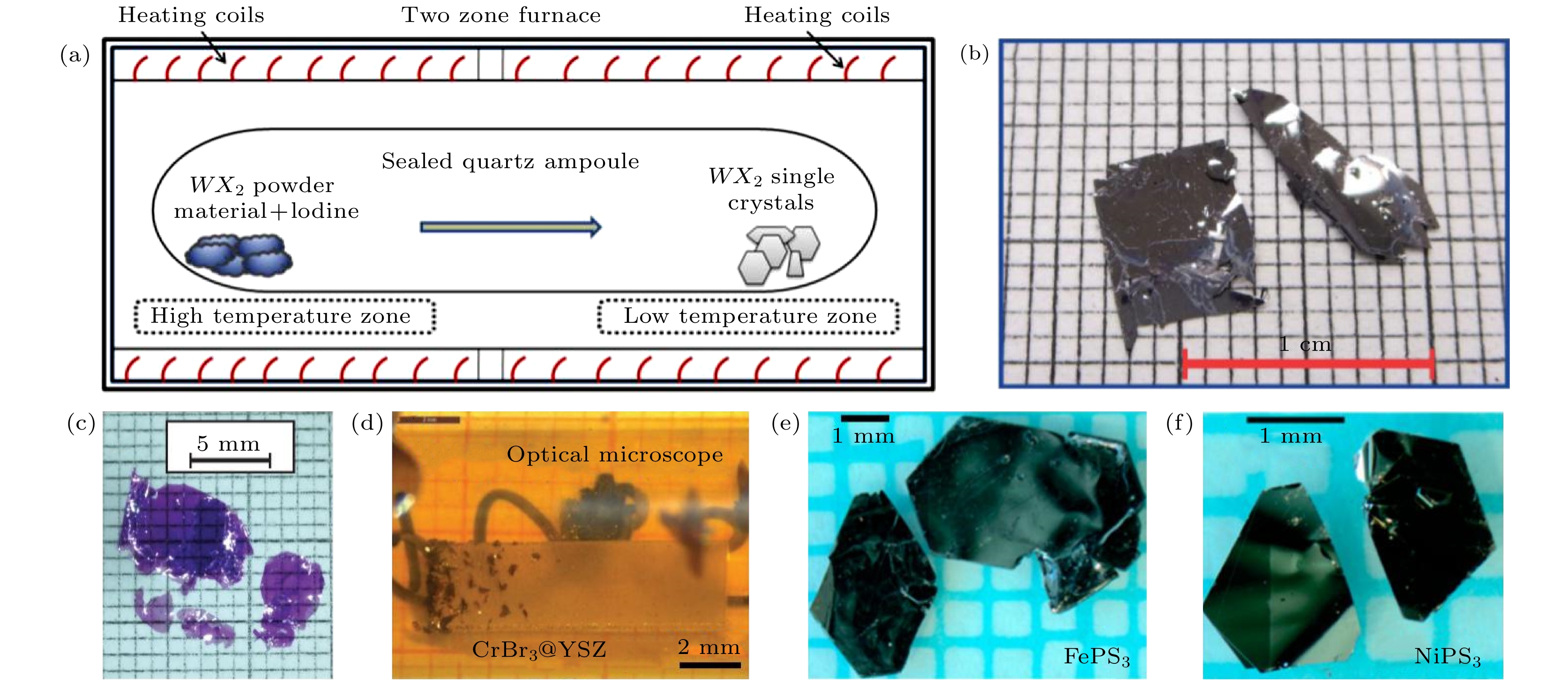
图 1 化学气相传输法制备块体晶体 (a)化学气相传输法生长块状单晶材料原理图; (b) CrI3单晶照片; (c) CrCl3单晶照片; (d) CrBr3单晶照片; (e) FePS3单晶照片; (f) NiPS3单晶照片. 数据来源于参考文献[48—51]
Figure 1. Sythesizing bulk crystal via chemical vapor transportation technology: (a) The scheme of chemical vapor transportation; (b) the optical photo of CrI3; (c) the optical photo of CrCl3; (d) the optical photo of CrBr3; (e) the optical photo of FePS3; (f) the optical photo of NiPS3. Data from Ref. [48–51].
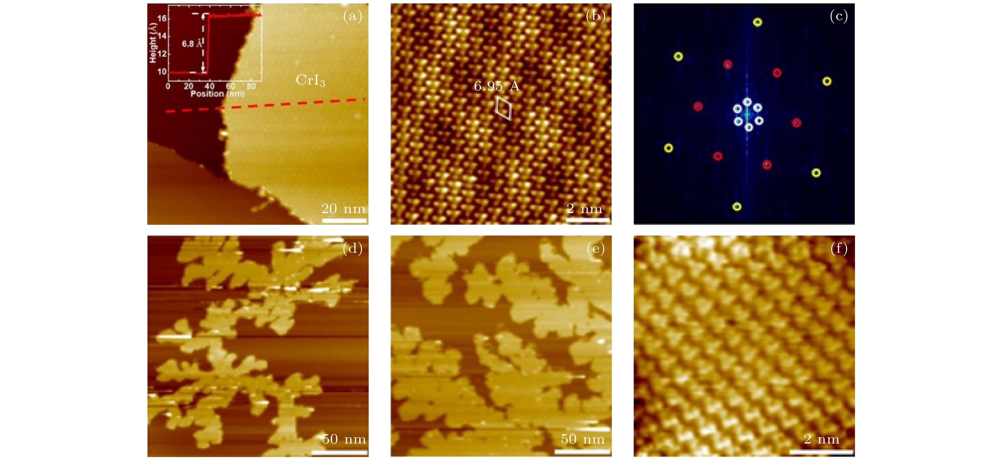
图 2 在Au (111)及HOPG基底上生长单层CrI3 (a) Au (111)表面单层CrI3的STM图像(插图为单层高度图); (b) 原子分辨的STM图像; (c)傅里叶变换图; (d)在HOPG上生长20 min的单层CrI3的大范围STM图像; (e)在HOPG上生长40 min的单层CrI3的大范围STM图像; (f)原子分辨图像; 数据来源于参考文献[53]
Figure 2. Growing monolayer CrI3 on Au (111) and HOPG substrates: (a) STM image of CrI3 monolayer on Au (111) substrate (the inset is a height profile along the red dashed line); (b) atomic-resolution STM image; (c) Fourier transform map of monolayer CrI3 on Au (111) substrate; STM images after (d) 20 min, (e) 40 min, andatomic-resolution image (f) of CrI3 on HOPG substrate. Data from Ref. [53].

图 3 MOKE显微镜装置搭建图. 633 nm的激光由He-Ne激光器发出, 采用机械斩波器和光弹性调制器分别进行光强调制和偏振调制. 调制的光束通过偏振分束器定向到样品中, 样品被放置在15 K的封闭循环低温恒温器中, 使用7 T螺线管超导磁体对样品施加磁场. 反射光束通过一个分析器到一个光电二极管上进行测量反射强度和克尔旋转角. 数据来源于参考文献[19].
Figure 3. Schematic of MOKE microscopy setup. A power-stabilized He-Ne laser (633 nm) is used for the optical excitation. A mechanical chopper and photoelastic modulator modulate the intensity and polarization of the exciting beam. The modulated beam is then conducted to the sample through a polarizing beam splitter. The sample is subjected to cryostat at T = 15 K with magnetic field upto 7 T. A lock in amplifier is used to detect the intensity and Kerr rotation of the reflected beam. Schematic of the setup from Ref. [19].

图 4 MOKE测量揭示单层CrI3晶体的铁磁性 (a) 单层CrI3的MOKE信号随磁场的变化; (b) 不同激光强度的MOKE信号, 其中蓝色、粉色和红色曲线对应的激光强度分别为3, 10 和30 μW; (c) 不同磁场下MOKE信号对温度的依赖关系, 其中红色曲线为磁场为0时的信号, 蓝色曲线为磁场为0.15 T时的信号; 数据来源于参考文献[19]
Figure 4. MOKE measurements of monolayer CrI3: (a) MOKE signal for a CrI3 monolayer varies with magnetic field; (b) power dependence of the MOKE signal taken at incident powers of 3 μW (blue), 10 μW (pink), and 30 μW (red); (c) temperature dependence of MOKE signal with the sample initially cooled at μ0H = 0 (blue) and 0.15 T (red). Data from Ref. [19].
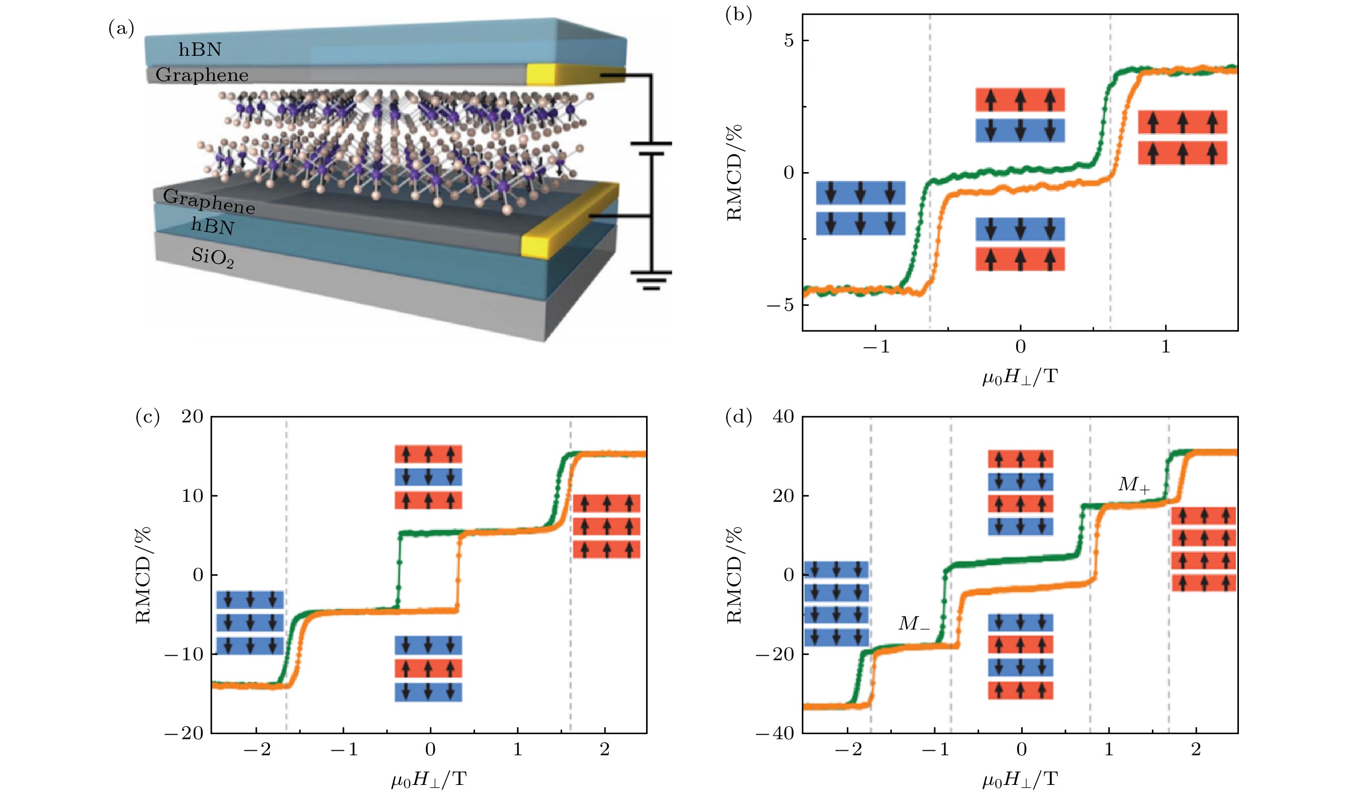
图 5 利用磁圆二色谱探测原子级厚度CrI3晶体中的磁序随外加磁场的变化 (a) 多层CrI3隧穿器件示意图; 温度为2 K 下, 双层(b)、三层(c)和四层(d) CrI3的RMCD信号对磁场的变化关系. 数据来源于参考文献[63]
Figure 5. Probing magnetism of atomic CrI3 via RMCD: (a) Schematic of two-dimensional spin-filter magnetic tunnel junction; magnetic field dependent RMCD signal of (b) bilayer, (c) trilayer and (d) four-layer CrI3 devices at T = 2 K. Data from Ref. [63].

图 6 自旋过滤效应探测原子级厚度CrI3晶体中磁序随磁场的变化 (a) 金属/铁磁绝缘体/金属隧穿结的能量示意图, 其中势垒区域的红线和蓝线分别表示自旋向上和自旋向下的势垒; (b) 石墨/CrI3/石墨隧穿结器件照片和示意图; (c) 双层CrI3的隧穿电导对磁场的依赖关系; 自旋向上电子和自旋向下电子隧穿经过双层反铁磁(d)和铁磁(e) CrI3时的势垒; (f) 四层CrI3的隧穿电导随磁场的变化; 自旋向上电子和自旋向下电子隧穿经过四层反铁磁(g)和铁磁(h) CrI3时的势垒; 数据来源于参考文献[29]
Figure 6. Probing the magnetism in atomically-thin CrI3 via spin filter effect. (a) Energy digram of metal/ferromagnetic insulator/ metal junction. The blue and red horizontal lines stand for the energy barriers of spin up and spin down as indicated by the red and blue arrows. (b) Optical picture and structure diagram of a graphite/tetralayer CrI3/graphite tunnel junction device. (c) Tunneling conductance of bilayer CrI3 device. The insets indicate the corresponding magnetic configurations. (d) and (e) The diagram of layer resolved, spin dependent tunneling barrier in antiferromagnetic phase (d) and in ferromagnetic phase (e). (f)–(h) Analogous data and schematics for tetralayer CrI3 device. Data from Ref. [29].

图 7 静电掺杂调控CrI3晶体磁结构 (a) Huang等[64]构筑的双栅极双层CrI3器件示意图; (b)在温度为15 K时, 同一器件的RMCD信号与磁场的关系, 掺杂水平约从0(黑色)到4.4 × 1012 cm–2 (红色); (c) 同掺杂水平, 在从0 V·nm–1 (红色)到0.6 V·nm–1(黑色)不等的几个外加场的作用下RMCD信号与磁场的关系; (d) Jiang等[20]构筑的双栅极双层CrI3场效应器件示意图; (e) 4 K时单层CrI3中饱和磁化强度、矫顽磁场和居里温度随电子掺杂水平和栅极电压的变化; (f) 4 K时双层CrI3掺杂密度-磁场强度相图, 左轴为栅极电压, 右轴为掺杂密度, FM和AFM相分别对应高、低RMCD信号的区域. 数据来源于参考文献[20,64].
Figure 7. Manipulating the magnetism of two-dimensional CrI3 crystals via electrostatic doping: (a) Schematic of a dual-gate bilayer CrI3 device fabricated by Huang et al.[64]; (b) RMCD signal of the same device varies with magnetic field at varying doping levels from 0 (black) to 4.4
$ \times $ 1012 cm–2 (red) with temperature fixed at T = 15 K; (c) the dependences of RMCD signal on magnetic field for displacement field varying from 0 V·nm–1 (red) to 0.6 V·nm–1 (black) with doping level fixed at zero; (d) schematic of a dual-gate bilayer CrI3 device fabricated by Jiang et al.[20]; (e) normalized Coercive field (magenta), saturation magnetization (purple) measured at T = 4 K and curie temperature (orange) to their values at zero gate voltage as functions of gate voltage (bottom axis) and doping density (top axis); (f) magnetic field-doping density phase diagram at T = 4 K. Data from Ref. [20,64].
图 8 电场通过磁电效应调节CrI3晶体的磁性 (a) 单层和双层CrI3原子结构图; (b) 双层AFM相CrI3电场诱导产生净磁示意图; (c) 4 K时MCD信号在不同外加电场下与磁场的关系; (d) 4 K时不同磁场下电场产生的磁化强度ΔM, 以及相对磁化强度ΔM/M0关于外加电场的关系; (e) 4 K温度下磁化强度对外加电场变化率随磁场的变化; (f) 双层CrI3的磁化强度M和归一化磁化强度M/M0在两个固定磁场(± 0.44 T下)与外加电场的关系图. 数据来源于参考文献 [67]
Figure 8. Control the magnetism of CrI3 via magnetoelectric effect: (a) Top view of monolayer (left panel) and side view of bilayer (right panel) CrI3 crystal; (b) antiferromagnetic bilayer CrI3 consists of two individual ferromagnetic monolayers with antiferromagnetic interlayer couplings. Schematic of nonzero net magnetization induced by electric field in bilayer CrI3 crystals; (c) MCD signal varies with magnetic field at different displacement electric field as indicated in the legends. The black and red curves stand for forward and backward sweeps of magnetic field; (d) electric field induced relative (left axis) and absolute (right axis) of magnetization as function of electric field at T = 4 K; (e) change rate of magnetization with displacement electric field as a function of magnetic field for bilayer and monolayer CrI3 flakes at 4 K; (f) absolute and relative magnetization of bilayer CrI3 as a function of electric field at fixed vertical magnetic field (filled: 0.44 T; empty: -0.44 T). Data from Ref. [67].
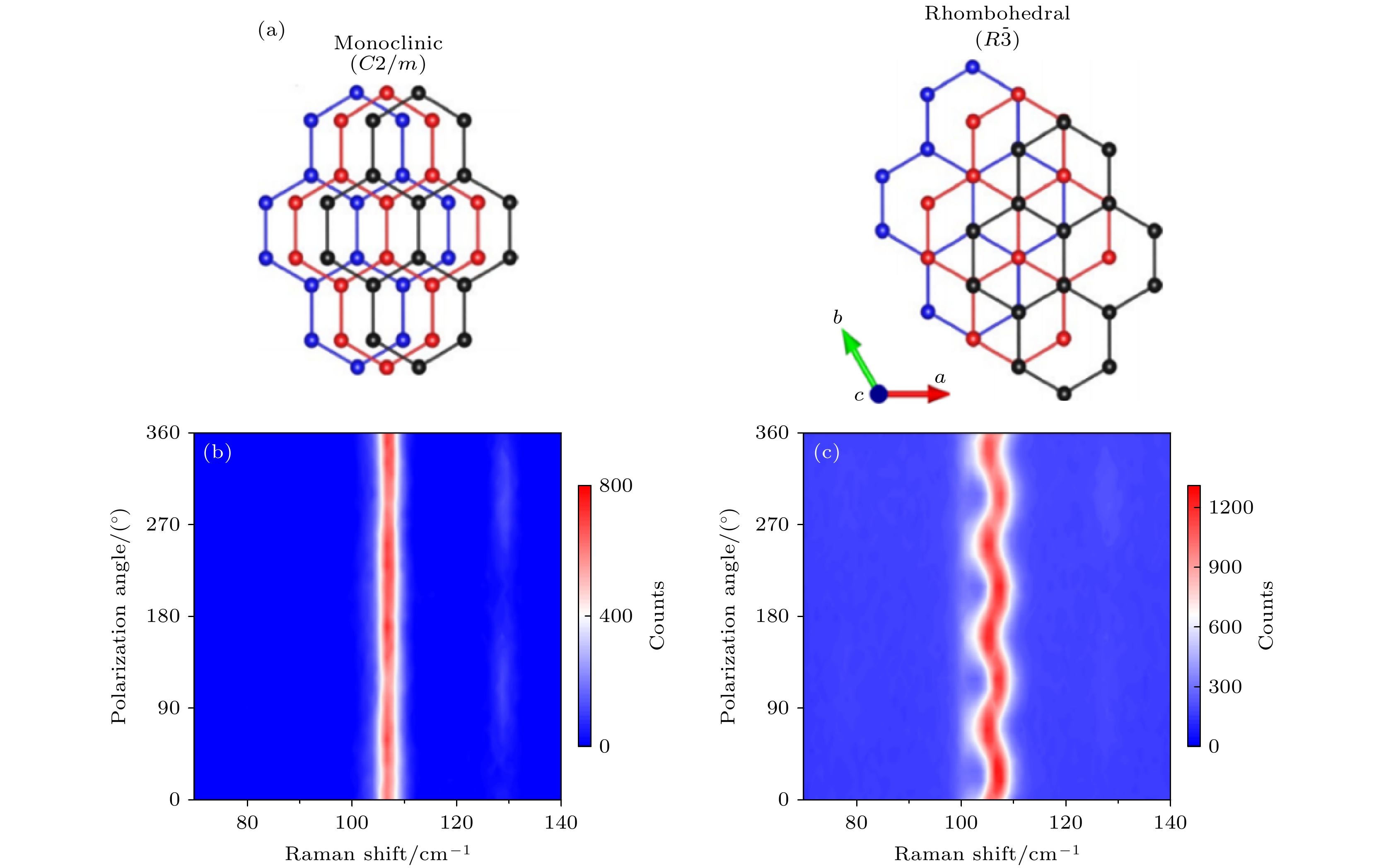
图 9 拉曼光谱揭示静压力引起的隧穿器件中CrI3 堆叠方式的变化 (a) 单斜相和三方相CrI3的层间堆叠顺序, 蓝色、红色和黑色球分别代表不同层中的Cr原子; (b) 单斜相CrI3的偏振拉曼光谱; (c) 三方相CrI3的偏振拉曼光谱. 数据来源于参考文献[30]
Figure 9. Raman spectrum reveal the change of CrI3 layer stacking order in tunneling devices: (a) Monoclinic (left panel) and rhombohedral (right panel) crystals order of CrI3; (b), (c) polarization dependences of Raman spectrum of CrI3 in monoclinic and rhombohedral phases respectively. Data from Ref. [30].
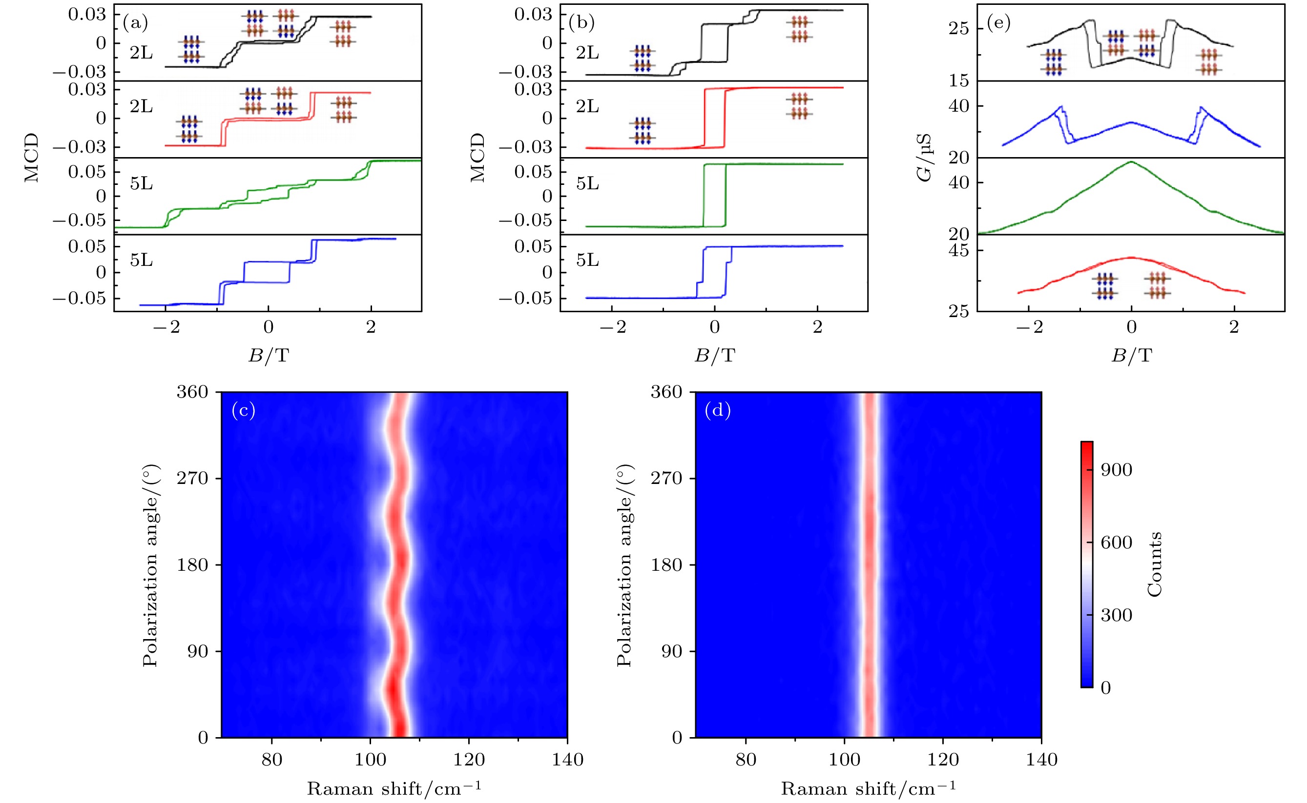
图 10 施加压力前后磁圆二色谱、偏振拉曼和隧穿电导的变化 (a) 施加1.8 GPa压力前两层和五层CrI3的MCD图像; (b)施加1.8 GPa压力后两层和五层CrI3的MCD图像; (c), (d) 在温度为300 K时, 施加1.8 GPa 静压力之前(c)与之后(d)五层CrI3拉曼光谱随偏转角度的变化; (e)温度为1.7 K时, 施加压力为0, 1, 1.8, 0 GPa (从上到下)时双层CrI3隧穿结器件的隧穿电导随磁场强度的变化图像; 数据来源于参考文献[30].
Figure 10. Comparing the MCD signal, polarized Raman spectrum and tunneling conductance before and after applying a high pressure: MCD signals of bilayer and five layer CrI3 crystals before (a) and after (b) applying the pressure; polarized Raman spectrum of five-layer CrI3 before (c) and after (d) applying a pressure of 1.8 GPa; (e) tunneling conductance of bilayer CrI3 device at pressure of 0, 1, 1.8 and 0 GPa (from top panel to bottom panel) at T = 1.7 K. Data from Ref. [30].
-
[1] Novoselov K S, Geim A K, Morozov S V 2004 Science 306 666
Google Scholar
[2] Kadantsev E S, Hawrylak P 2012 Solid State Commun. 152 909
Google Scholar
[3] Miró P, Ghorbani-Asl M, Heine T 2013 Adv. Mater. 25 5473
Google Scholar
[4] Splendiani A, Sun L, Zhang Y 2010 Nano Lett. 10 1271
Google Scholar
[5] Yoon Y, Ganapathi K, Salahuddin S 2011 Nano Lett. 11 3768
Google Scholar
[6] Liu W, Kang J, Sarkar D 2013 Nano Lett. 13 1983
Google Scholar
[7] Zhao W, Ghorannevis Z, Chu L 2013 ACS Nano 7 791
Google Scholar
[8] Ling X, Wang H, Huang S 2015 Proc. Natl. Acad. Sci. 112 4523
Google Scholar
[9] Li L, Yu Y, Ye G J 2014 Nat. Nanotechnol. 9 372
Google Scholar
[10] Liu L, Feng Y P, Shen Z X 2003 Phy. Rev. B 68 104102
Google Scholar
[11] Song L, Ci L, Lu H 2010 Nano Lett. 10 3209
Google Scholar
[12] Gupta A, Sakthivel T, Seal S 2015 Prog. Mater. Sci. 73 44
Google Scholar
[13] Zhang J L, Han C, Hu Z 2018 Adv. Mater. 30 1802207
Google Scholar
[14] Mak K F, Shan J 2016 Nat. Photonics 10 216
Google Scholar
[15] Roy P K, Luxa J, Sofer Z 2020 Nanoscale 12 10430
Google Scholar
[16] Mermin N D, Wagner H 1966 Phys. Rev. Lett. 17 1133
Google Scholar
[17] Irkhin V Y, Katanin A A 1999 Phys. Rev. B 60 2990
Google Scholar
[18] Gong C, Li L, Li Z, Ji H W, Stern A, Xia Y, Cao T, Bao W, Wang C Z, Wang Y, Qiu Z Q, Cava R J, Louie S G, Xia J, Zhang X 2017 Nature 546 265
Google Scholar
[19] Huang B, Clark G, Navarro-Moratalla E, Klein D R, Cheng R, Seyler K L, Zhong D, Schmidgall E, McGuire M A, Cobden D H, Yao W, Xiao D, Jarillo-Herrero P, Xu X D 2017 Nature 546 270
Google Scholar
[20] Jiang S, Li L, Wang Z 2018 Nat. Nanotechnol. 13 549
Google Scholar
[21] Baidya S, Yu J, Kim C H 2018 Phys. Rev. B 98 155148
Google Scholar
[22] Zhao Y, Lin L, Zhou Q 2018 Nano Lett. 18 2943
Google Scholar
[23] Huang B, Cenker J, Zhang X 2020 Nat. Nanotechnol. 15 212
Google Scholar
[24] Zhu M, Yao H, Jiang L 2020 Appl. Phys. Lett. 116 022404
Google Scholar
[25] Seyler K L, Zhong D, Klein D R 2018 Nat. Phys. 14 277
Google Scholar
[26] Sun Z, Yi Y, Song T 2019 Nature 572 497
Google Scholar
[27] Jin W, Kim H H, Ye Z 2020 Nat. Commun. 11 4780
Google Scholar
[28] Mukherjee A, Shayan K, Li L 2020 Nat. Commun. 11 5502
Google Scholar
[29] Klein D R, MacNeill D, Lado J L 2018 Science 360 1218
Google Scholar
[30] Li T, Jiang S, Sivadas N 2019 Nat. Mater. 18 1303
Google Scholar
[31] Wang Z, Gibertini M, Dumcenco D 2019 Nat. Nanotechnol. 14 1116
Google Scholar
[32] Jiang S, Li L, Wang Z 2019 Nat. Electron. 2 159
Google Scholar
[33] Kim H H, Jiang S, Yang B 2020 Adv. Mater. 32 1905433
Google Scholar
[34] Wang Z, Gutiérrez-Lezama I, Ubrig N, Kroner M, Gibertini M, Taniguchi T, Watanabe K, Imamog˘lu A, Giannini E, Morpurgo A F 2018 Nat. Commun. 9 2516
Google Scholar
[35] McGuire M A, Dixit H, Cooper V R 2015 Chem. Mater. 27 612
Google Scholar
[36] Yang W, Chen G, Shi Z 2013 Nat. Mater. 12 792
Google Scholar
[37] Zhang J, Yu H, Chen W 2014 ACS Nano 8 6024
Google Scholar
[38] Wang Q, Li N, Tang J 2020 Nano Lett. 20 7193
Google Scholar
[39] Huang Y, Pan Y H, Yang R 2020 Nat. Commun. 11 2453
Google Scholar
[40] Li H, Wu J, Yin Z 2014 Acc. Chem. Res. 47 1067
Google Scholar
[41] Velický M, Toth P S, Rakowski A M 2017 Nat. Commun. 8 1
Google Scholar
[42] Nakano M, Wang Y, Kashiwabara Y 2017 Nano Lett. 17 5595
Google Scholar
[43] Yuan X, Tang L, Liu S 2015 Nano Lett. 15 3571
Google Scholar
[44] Hao W, Marichy C, Journet C 2019 2D Mater. 6 012001
Google Scholar
[45] Cai J, Han X, Wang X 2020 Matter 2 587
Google Scholar
[46] Levita G, Restuccia P, Righi M C 2016 Carbon 107 878
Google Scholar
[47] Zacharia R, Ulbricht H, Hertel T 2004 Phys. Rev. B 69 155406
Google Scholar
[48] Habib M, Muhammad Z, Khan R 2018 Nanotechnology 29 115701
Google Scholar
[49] McGuire M A, Clark G, Santosh K C, Chance W M, Jellison G. E, Cooper V R, Xu X, Sales B C 2017 Phys. Rev. Mater. 1 014001
Google Scholar
[50] Grönke M, Buschbeck B, Schmidt P, Valldor M, Oswald S, Hao Q, Lubk A, Wolf D, Steiner U, Büchner B, Hampel S 2019 Adv. Mater. Interfaces 6 1901410
Google Scholar
[51] Du K, Wang X, Liu Y 2016 ACS Nano 10 1738
Google Scholar
[52] Kim H H, Yang B, Li S, Jiang S W, Jin C H, Tao Z, Nichols G, Sfigakis F, Zhong S Z, Li C, Tian S J, Cory D, Miao G X, Shan J, Mak K F, Lei H C, Sun K, Zhao L Y, Tsen A 2019 Proc. Natl. Acad. Sci. 116 11131
Google Scholar
[53] Li P, Wang C, Zhang J H, Chen S W, Guo D H, Ji W, Zhong D Y 2020 Sci. Bull. 65 1064
Google Scholar
[54] Chen W J, Sun Z Y, Wang Z J, Gu L H, Xu X D, Wu S W, Gao C L 2019 Science 366 983
Google Scholar
[55] Nakano M, Wang Y, Yoshida S, Mastsuoka H, Majima Y, Ikeda K, Hirata Y, Takeda Y, Wadati H, Kohama Y, Ohigashi Y, Sakano M, Ishizaka K, Iwasa Y 2019 Nano Lett. 12 8806
[56] Liu S, Yuan X, Zhou Y 2017 NPJ 2D Mater. Appl. 1 30
Google Scholar
[57] Thiel L, Wang Z, Tschudin M A, Rohner D, Gutiérrez-Lezama I, Ubrig N, Gibertini M, Giannini E, Morpurgo A F, Maletinsky P 2019 Science 364 973
Google Scholar
[58] Mak K F, Shan J, Ralph D C 2019 Nat. Rev. Phys. 1 646
Google Scholar
[59] Jiang S, Xie H, Shan J 2020 Nat. Mater. 19 1295
Google Scholar
[60] Song T, Fei Z, Yankowitz M 2019 Nat. Mater. 18 1298
Google Scholar
[61] Wang X, Du K, Liu Y Y F 2016 2D Mater. 3 031009
Google Scholar
[62] Long G, Henck H, Gibertini M 2020 Nano Lett. 20 2452
Google Scholar
[63] Song T, Cai X, Tu M W Y 2018 Science 360 1214
Google Scholar
[64] Huang B, Clark G, Klein D R 2018 Nat. Nanotechnol. 13 544
Google Scholar
[65] Fallahazad B, Movva H C P, Kim K, Larentis S, Taniguchi T, Watanabe K, Banerjee S K, Tutuc E 2016 Phys. Rev. Lett. 116 086601
Google Scholar
[66] Wang H, Eyert V, Schwingenschlögl U 2011 J. Phys. Condens. Matter. 23 116003
Google Scholar
[67] Jiang S, Shan J, Mak K F 2018 Nat. Mater. 17 406
Google Scholar
[68] Arima T H 2008 J. Phys. Condens. Matter. 20 434211
Google Scholar
[69] Fiebig M 2005 J. Phys. D 38 R123
Google Scholar
[70] Eerenstein W, Mathur N D, Scott J F 2006 Nature 442 759
Google Scholar
[71] Jacobs I S, Lawrence P E 1967 Phys. Rev. 164 866
Google Scholar

 DownLoad:

Catalog
Metrics
- Abstract views: 10580
- PDF Downloads: 957
- Cited By: 0
