


-
The interplay between non-trivial band topology and magnetic order can induce exotic quantum phenomena, such as the quantum anomalous Hall effect and axion insulator state. A prevalent approach to realizing such topological states is either by magnetic doping or through heterostructure engineering, while the former will bring in inhomogeneity and the latter requires complex procedures. Intrinsic magnetic topological insulators are expected to avoid the aforementioned disadvantages, which is of great significance in both studying and practically using these exotic quantum phenomena. Recently, a Zintl compound EuIn2As2 is predicted to be an intrinsic antiferromagnetic axion insulator. The bulk magnetic order of EuIn2As2 has been reported in a lot of experiments, while the topological nature has not yet been confirmed. The surface properties of intrinsic magnetic topological insulators play an important role in the interplay between magnetic order and non-trivial surface state. Here in this work, we study the surface structure and electronic property of EuIn2As2 single crystal by using scanning tunneling microscopy/spectroscopy (STM/S) and non-contact atomic force microscopy (NC-AFM). Considering the strength of bonds, the easy cleavage plane of the crystals possibly lies between In-In layers or between Eu-As layers. The STM topographies show that the cleaved surface is dominated by a striped pattern. And the dominated step height is an integer multiple of c/2, which implies that only one kind of cleavage plane is preferred. Atomic-resolved surface topographies show that the striped pattern is the
$ 1\times 2 $ surface reconstruction with 50% coverage. Hence an In-terminated surface which will be 100% coverage is ruled out. The spatial evolution of STS near vacancies on the striped pattern shows a hole-doping feature. All of these results reveal that the striped pattern is the$ 1\times 2 $ surface reconstruction of the Eu terminated surface with 50% coverage. Using the STS, we measure the local densities of states on the striped surface at various temperatures. We find that there is an asymmetric valley-peak feature in the density of states near the Fermi energy at 4 K, which is gradually weakened with increasing temperature, and disappears above the antiferromagnetic Néel temperature, indicating that the asymmetric valley-peak feature is closely related to the antiferromagnetic order. Besides, a maze-like pattern is observed occasionally near some step edges. The STM topographies show atoms both on bright and dark stripes of the maze-like pattern, which form a whole hexagonal lattice. And the NC-AFM images show that the maze-like pattern is about 1 Å higher than the Eu terminated striped pattern. Based on these results, the maze-like pattern can be explained as the buckled Eu surface with 100% coverage. These results provide important information for understanding the surface electronic band structure and topological nature of EuIn2As2.-
Keywords:
- scanning tunneling microscopy /
- EuIn2As2 /
- magnetic topological insulator /
- surface reconstruction
[1] Tokura Y, Yasuda K, Tsukazaki A 2019 Nat. Rev. Phys. 1 126
 Google Scholar
[2] Yu R, Zhang W, Zhang H J, Zhang S C, Dai X, Fang Z 2010 Science 329 61
Google Scholar
[3] Nenno D M, Garcia C A C, Gooth J, Felser C, Narang P 2020 Nat. Rev. Phys. 2 682
Google Scholar
[4] Qi X L, Hughes T L, Zhang S C 2010 Phys. Rev. B 82 184516
Google Scholar
[5] Liu Q, Liu C X, Xu C, Qi X L, Zhang S C 2009 Phys. Rev. Lett. 102 156603
Google Scholar
[6] Katmis F, Lauter V, Nogueira F S, Assaf B A, Jamer M E, Wei P, Satpati B, Freeland J W, Eremin I, Heiman D, Jarillo-Herrero P, Moodera J S 2016 Nature 533 513
Google Scholar
[7] Li J, Li Y, Du S, Wang Z, Gu B L, Zhang S C, He K, Duan W, Xu Y 2019 Sci. Adv. 5 eaaw5685
Google Scholar
[8] Deng Y, Yu Y, Shi M Z, Guo Z, Xu Z, Wang J, Chen X H, Zhang Y 2020 Science 367 895
Google Scholar
[9] Liang Z, Luo A, Shi M, Zhang Q, Nie S, Ying J J, He J F, Wu T, Wang Z, Xu G, Wang Z, Chen X H 2020 Phys. Rev. B 102 161115
Google Scholar
[10] Xu Y, Song Z, Wang Z, Weng H, Dai X 2019 Phys. Rev. Lett. 122 256402
Google Scholar
[11] Li H, Gao S Y, Duan S F, Xu Y F, Zhu K J, Tian S J, Gao J C, Fan W H, Rao Z C, Huang J R, Li J J, Yan D Y, Liu Z T, Liu W L, Huang Y B, Li Y L, Liu Y, Zhang G B, Zhang P, Kondo T, Shin S, Lei H C, Shi Y G, Zhang W T, Weng H M, Qian T, Ding H 2019 Phys. Rev. X 9 041039
Google Scholar
[12] Gui X, Pletikosic I, Cao H, Tien H J, Xu X, Zhong R, Wang G, Chang T R, Jia S, Valla T, Xie W, Cava R J 2019 ACS Cent. Sci. 5 900
Google Scholar
[13] Zhang Y, Deng K, Zhang X, Wang M, Wang Y, Liu C, Mei J W, Kumar S, Schwier E F, Shimada K, Chen C, Shen B 2020 Phys. Rev. B 101 205126
Google Scholar
[14] Goforth A M, Klavins P, Fettinger J C, Kauzlarich S M 2008 Inorg. Chem. 47 11048
Google Scholar
[15] Yu F H, Mu H M, Zhuo W Z, Wang Z Y, Wang Z F, Ying J J, Chen X H 2020 Phys. Rev. B 102 180404
Google Scholar
[16] Rosa P F S, Adriano C, Garitezi T M, Ribeiro R A, Fisk Z, Pagliuso P G 2012 Phys. Rev. B 86 094408
Google Scholar
[17] Riberolles S X M, Trevisan T V, Kuthanazhi B, Heitmann T W, Ye F, Johnston D C, Bud’ko S L, Ryan D H, Canfield P C, Kreyssig A, Vishwanath A, McQueeney R J, Wang L L, Orth P P, Ueland B G 2021 Nat. Commun. 12 999
Google Scholar
[18] Sato T, Wang Z, Takane D, Souma S, Cui C, Li Y, Nakayama K, Kawakami T, Kubota Y, Cacho C, Kim T K, Arab A, Strocov V N, Yao Y, Takahashi T 2020 Phys. Rev. Res. 2 033342
Google Scholar
[19] Regmi S, Hosen M M, Ghosh B, Singh B, Dhakal G, Sims C, Wang B, Kabir F, Dimitri K, Liu Y, Agarwal A, Lin H, Kaczorowski D, Bansil A, Neupane M 2020 Phys. Rev. B 102 165153
Google Scholar
[20] Lv B Q, Weng H M, Fu B B, Wang X P, Miao H, Ma J, Richard P, Huang X C, Zhao L X, Chen G F, Fang Z, Dai X, Qian T, Ding H 2015 Phys. Rev. X 5 031013
Google Scholar
[21] Cao L, Song Y, Liu Y B, Zheng Q, Han G, Liu W, Li M, Chen H, Xing Y, Cao G H, Ding H, Lin X, Du S, Zhang Y Y, Li G, Wang Z, Gao H J 2021 Nano Res. DOI: 10.1007/s12274-021-3316-0
[22] Wiesendanger R, Bürgler D, Tarrach G, Güntherodt H J 1990 Surf. Sci. 232 1
Google Scholar
[23] Oura K, Lifshits V, Saranin A, Zotov A, Katayama M 2013 Surface Science: an Introduction (Berlin: Springer Science & Business Media) pp181−183
[24] Singh N, Schwingenschlögl U 2012 Appl. Phys. Lett. 100 151906
Google Scholar
[25] Nie S, Feenstra R M, Lee J Y, Kang M H 2004 J. Vac. Sci. Technol. A 22 1671
Google Scholar
[26] Gao M, Ma F, Lu Z Y, Xiang T 2010 Phys. Rev. B 81 193409
Google Scholar
[27] Mao H Q, Li N, Chen X, Xue Q K 2012 Chin. Phys. Lett. 29 066802
Google Scholar
[28] Denisov N V, Chukurov E N, Luniakov Y V, Utas O A, Azatyan S G, Yakovlev A A, Zotov A V, Saranin A A 2014 Surf. Sci. 623 17
Google Scholar
[29] Pai W W, Hsu C L, Lin M C, Lin K C, Tang T B 2004 Phys. Rev. B 69 125405
Google Scholar
[30] Ottaviano L, Ressel B, Di Teodoro C, Profeta G, Santucci S, Cháb V, Prince K C 2003 Phys. Rev. B 67 045401
Google Scholar
[31] Kawamura H 1998 J. Phys. Condens. Matter 10 4707
Google Scholar
[32] Zhou Y, Kanoda K, Ng T K 2017 Rev. Mod. Phys. 89 025003
Google Scholar
-
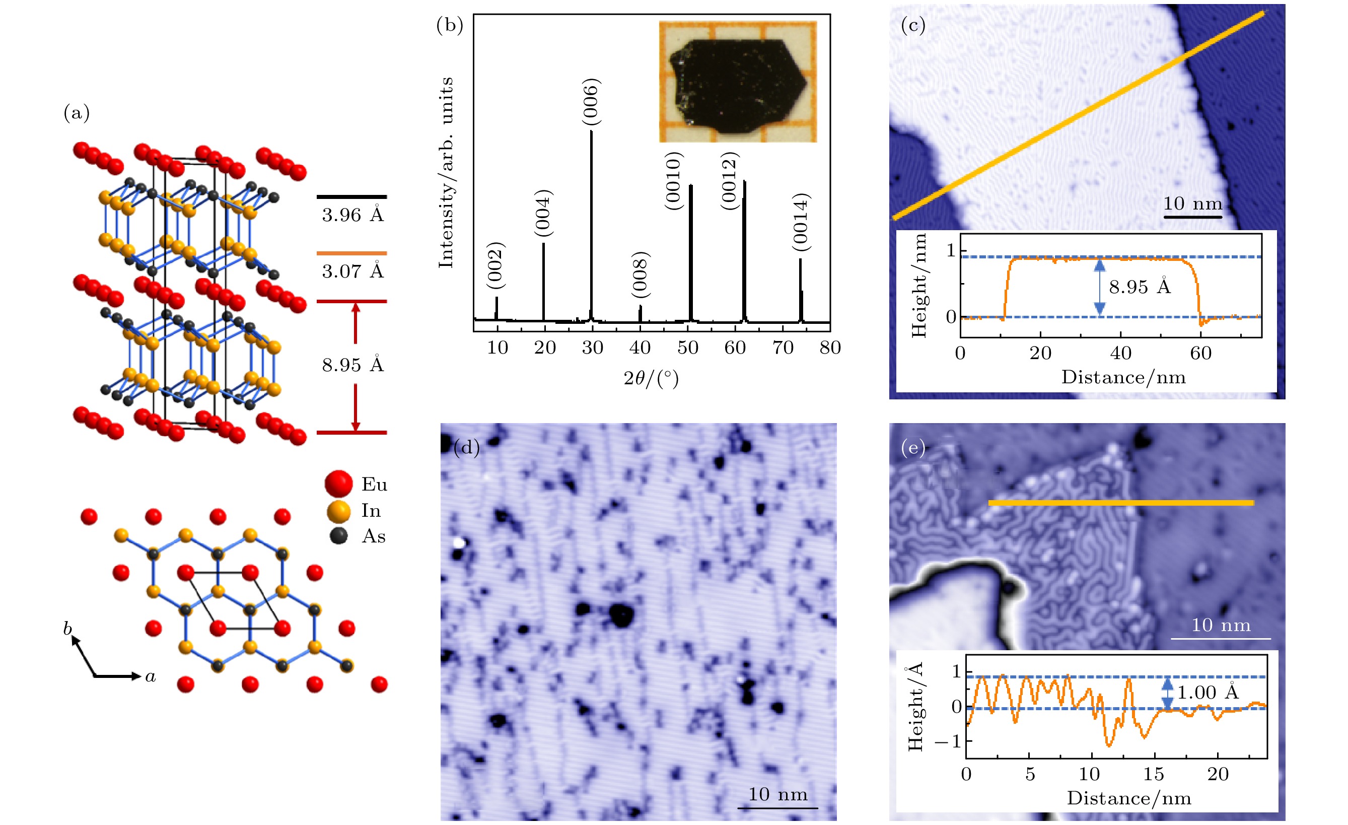
图 1 EuIn2As2的晶格结构和表面形貌 (a) EuIn2As2的晶格结构示意图, 图中所示Eu—Eu, Eu—In, In—As原子层间距分别是8.95, 3.07, 3.96 Å; (b) EuIn2As2的X射线衍射图案, 插图是典型EuIn2As2单晶的照片; (c) 包含台阶的大范围STM形貌图(Vs = 1 V, I = 100 pA), 插图是沿着图中黄线所标示位置的高度轮廓, 台阶高度8.95 Å, 与晶格常数的一半 c/2 = 8.95 Å 一致; (d) 典型的条纹面STM形貌(Vs = 1 V, I = 1 nA); (e) 包含迷宫状结构的STM形貌图 (Vs = –200 mV, I = 20 pA), 图中左下角为上层台阶, 右侧为条纹面, 插图是沿着图中黄线所标示位置的高度轮廓, 迷宫面与条纹面高度差约1 Å
Figure 1. Crystal structure and surface morphologies of EuIn2As2. (a) Schematic crystal structure of EuIn2As2, where the interlayer distance Eu—Eu, Eu—In, and In—As is 8.95, 3.07, and 3.96 Å, respectively. (b) X-ray diffraction pattern of EuIn2As2 crystal. The inset is a picture of typical EuIn2As2 single crystal. (c) Large scale STM topography showing step edges (Vs = 1 V, I = 100 pA). Inset is the height profile along yellow line, the step height is 8.95Å, which is consistent with half unit cell c/2 = 8.95 Å. (d) STM topography of typical stripe surface (Vs = 1 V, I = 1 nA). (e) STM topography containing a maze-like structure (Vs = –200 mV, I = 20 pA), which is located between a higher step (left bottom) and a stripe surface (right part). The inset is the height profile along yellow line. The step height between maze-like surface and stripe surface is about 1 Å.
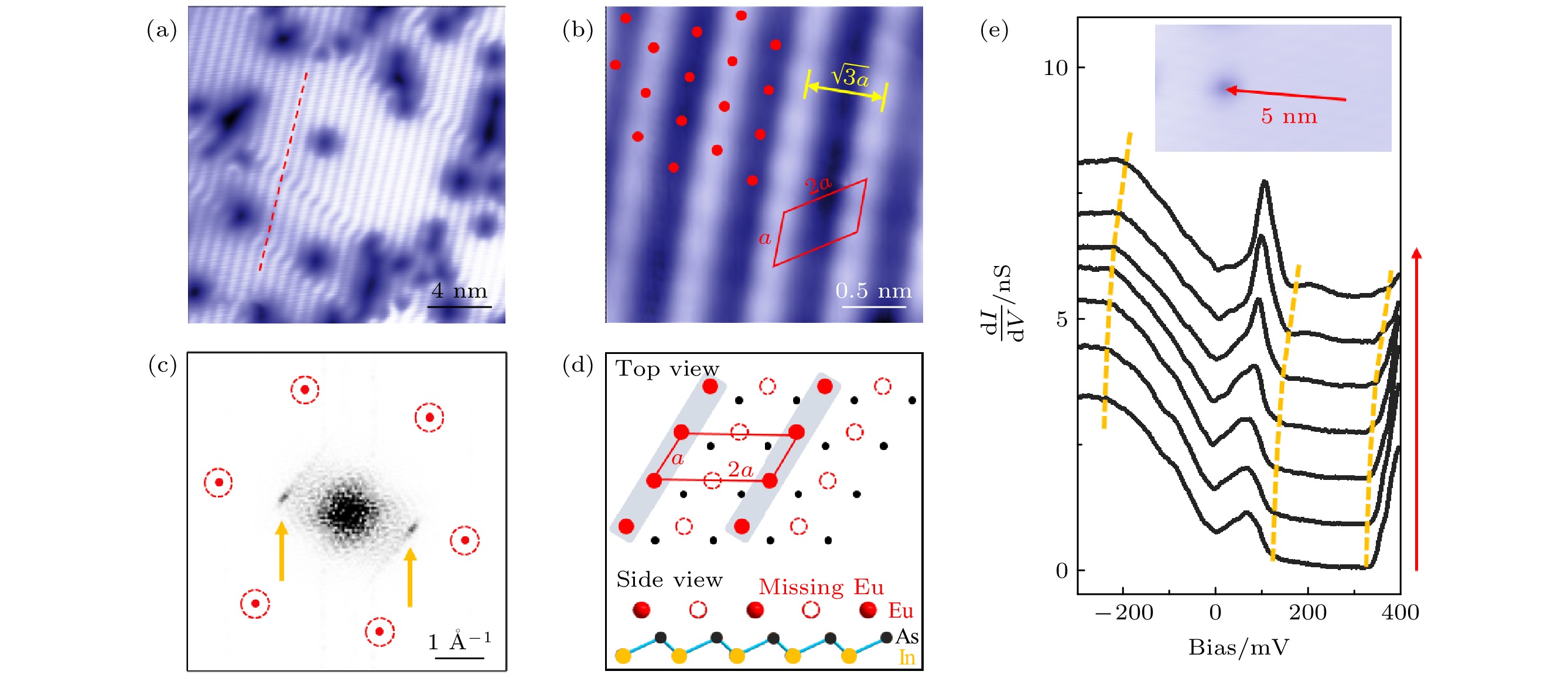
图 2 条纹面的结构 (a) 条纹面的STM形貌 (Vs = 1 V, I = 200 pA), 沿图中红色虚线条纹转折一次错位半个周期, 深蓝色区域为表面缺陷; (b) 条纹面的原子分辨像 (Vs = –2 mV, I = 1 nA), 红色平行四边形表示重构后的原胞, 红色点阵代表面内晶格格点; (c) 图(a)的FFT, 黄色箭头所示为条纹的周期, 红色圆圈标注的六个红点代表图(b)所标注六角格子的布拉格点; (d)条纹面的原子排布示意图, 暗红色球代表观测到的Eu原子, 红色虚线圆圈代表亮条纹之间丢失的Eu原子, 黑色/黄色点代表Eu层以下的As/In原子; (e)跨条纹面上空位缺陷的STS谱, 插图中红线标出了测谱位置, 测谱条件为Vs = 400 mV, I = 200 pA, 调制电压幅度5 mV, 图中黄色虚线帮助示意STS曲线中的特征随空间的演变
Figure 2. Structure of stripe surface. (a) STM topography of stripe surface (Vs = 1 V, I = 200 pA), the stripe shifts half unit cell along the red dashed line. Dark blue areas are surface defects. (b) Atomic resolved STM image of stripe surface (Vs = –2 mV, I = 1 nA), the red parallelogram shows the doubled unit cell, the red spots are superposed in-plane lattice structure. (c) FFT image of panel (a). The stripe modulation is marked by yellow arrows. The superposed six red dots marked by dashed red circles are the simulated Bragg points of the inserted hexagonal lattice in panel (b). (d) Schematic drawings of atomic arrangement on the stripe surface. Dark red spheres show the observed Eu atomic chain, dashed red circles show the missing Eu atoms between light stripes, black/yellow dots show the As/In atoms beneath the Eu layer. (e) STS taken across a vacancy in a stripe surface, the position is marked as the red line in the inset topographic image. Spectra are taken at Vs = 400 mV, I = 200 pA, with modulation 5 mV. The yellow dashed lines are guided for the spatial evolution of STS.
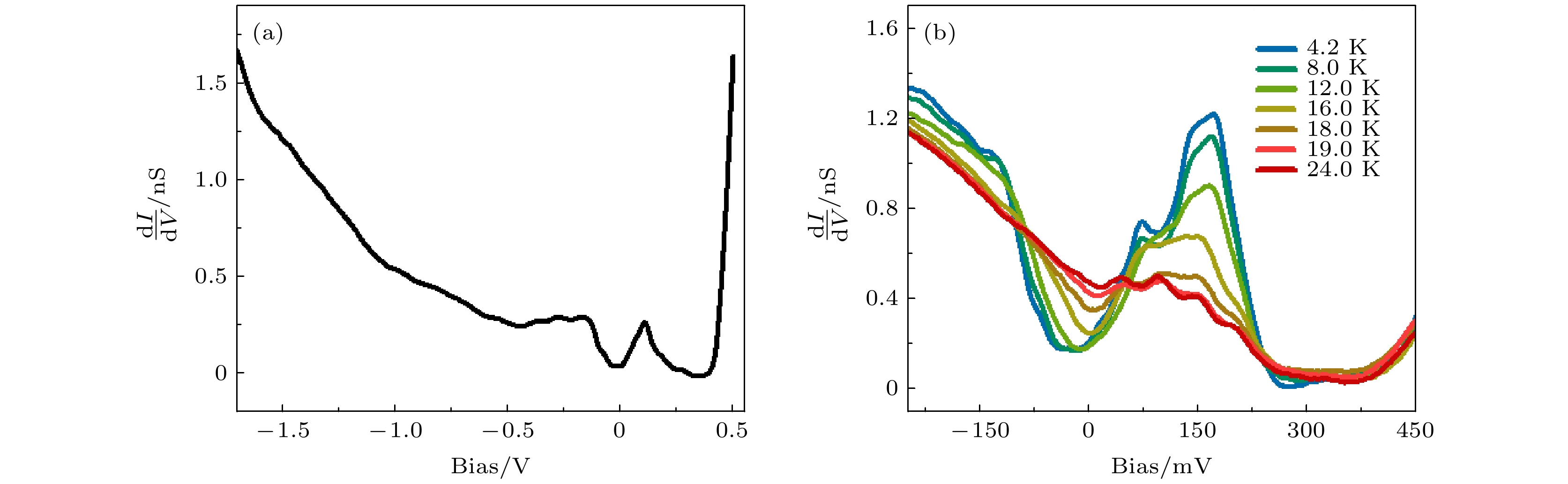
图 3 条纹面上的STS (a) 大能量范围的STS, 采谱条件为Vs = –1.7 V, I = 1 nA, 调制电压为10 mV; (b) 不同温度的STS, 采谱条件为Vs = –250 mV, I = 200 pA, 调制电压为5 mV
Figure 3. STS on stripe surface: (a) Large energy range STS, where the spectrum is taken at Vs = –1.7 V, I = 1 nA with modulation 10 mV; (b) STS taken at different temperatures, where the spectra are taken at Vs = –250 mV, I = 200 pA with modulation 5 mV.
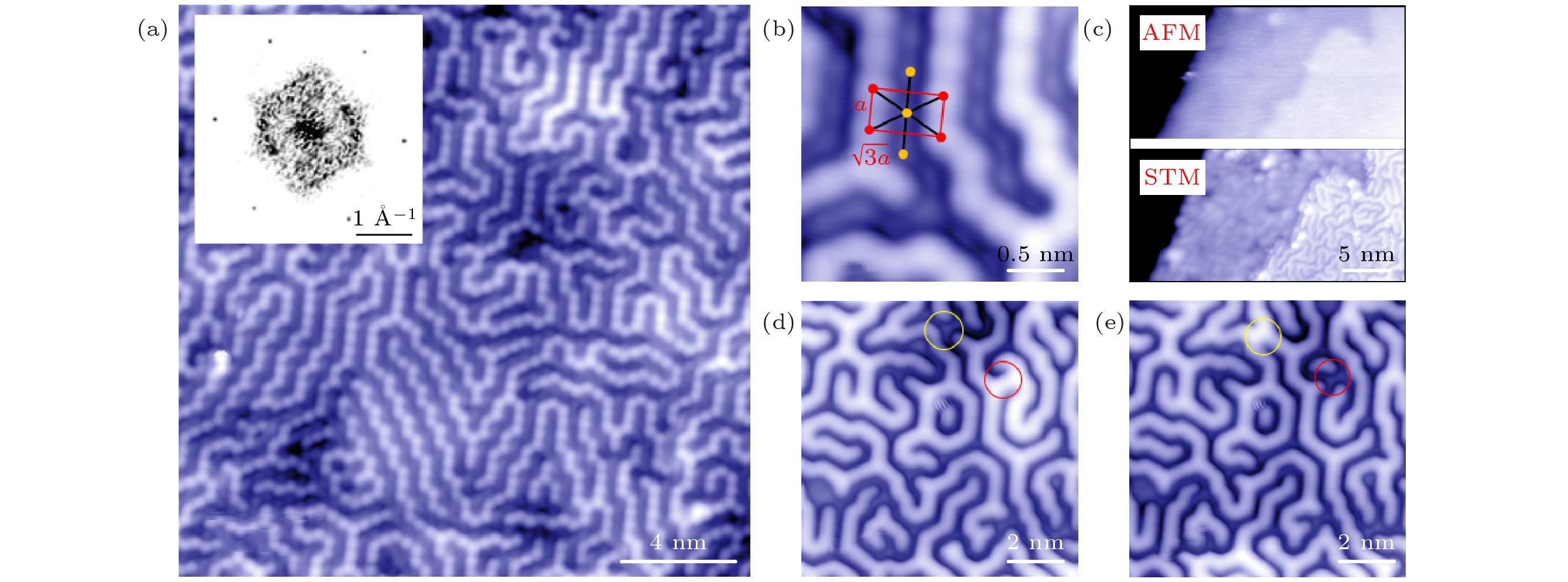
图 4 迷宫面的结构 (a) 迷宫面的原子分辨图 (Vs = 10 mV, I = 100 pA), 插图是相应的FFT图; (b) 小范围的原子分辨STM形貌图 (Vs = 10 mV, I = 100 pA), 暗条纹中可以看到清晰的原子, 原子位置图中用黄球标示; (c)迷宫面和条纹面台阶的AFM (上图)和STM (下图)形貌图, 图中左侧暗区为下层台面, 中部为条纹面, 最右侧为迷宫面, AFM/STM观测的台阶高度为1.1 Å/1.3 Å; (d), (e)迷宫面在电压脉冲下的不稳定性, 在(d)中红色圆圈内施加400 mV的电压脉冲, 表面原子排布变为(e)图所示, 其中黄圈位置的原子由暗变亮, 红圈位置的原子由亮变暗
Figure 4. Structure of the maze-like surface. (a) Atomic resolved STM image of maze-like surface (Vs = 10 mV, I = 100 pA), with corresponding FFT image inserted. (b) Small scale atomic resolved STM topography (Vs = 10 mV, I = 100 pA), atoms in the dark stripes, which are marked by yellow dots, are clearly visible. (c) AFM (up panel) and STM (down panel) topography of the step coexisting of maze (right) and stripe (middle) surface. Step height from AFM (STM) is 1.1 Å (1.3 Å). (d), (e) Surface topography evolution under a voltage pulse showing the metastability of the maze-like pattern. A 400 mV voltage pulse is applied in the red circle of panel (d), leading to a rearrangement of atoms in both red and yellow circles from panel (d) to panel (e).
-
[1] Tokura Y, Yasuda K, Tsukazaki A 2019 Nat. Rev. Phys. 1 126
Google Scholar
[2] Yu R, Zhang W, Zhang H J, Zhang S C, Dai X, Fang Z 2010 Science 329 61
Google Scholar
[3] Nenno D M, Garcia C A C, Gooth J, Felser C, Narang P 2020 Nat. Rev. Phys. 2 682
Google Scholar
[4] Qi X L, Hughes T L, Zhang S C 2010 Phys. Rev. B 82 184516
Google Scholar
[5] Liu Q, Liu C X, Xu C, Qi X L, Zhang S C 2009 Phys. Rev. Lett. 102 156603
Google Scholar
[6] Katmis F, Lauter V, Nogueira F S, Assaf B A, Jamer M E, Wei P, Satpati B, Freeland J W, Eremin I, Heiman D, Jarillo-Herrero P, Moodera J S 2016 Nature 533 513
Google Scholar
[7] Li J, Li Y, Du S, Wang Z, Gu B L, Zhang S C, He K, Duan W, Xu Y 2019 Sci. Adv. 5 eaaw5685
Google Scholar
[8] Deng Y, Yu Y, Shi M Z, Guo Z, Xu Z, Wang J, Chen X H, Zhang Y 2020 Science 367 895
Google Scholar
[9] Liang Z, Luo A, Shi M, Zhang Q, Nie S, Ying J J, He J F, Wu T, Wang Z, Xu G, Wang Z, Chen X H 2020 Phys. Rev. B 102 161115
Google Scholar
[10] Xu Y, Song Z, Wang Z, Weng H, Dai X 2019 Phys. Rev. Lett. 122 256402
Google Scholar
[11] Li H, Gao S Y, Duan S F, Xu Y F, Zhu K J, Tian S J, Gao J C, Fan W H, Rao Z C, Huang J R, Li J J, Yan D Y, Liu Z T, Liu W L, Huang Y B, Li Y L, Liu Y, Zhang G B, Zhang P, Kondo T, Shin S, Lei H C, Shi Y G, Zhang W T, Weng H M, Qian T, Ding H 2019 Phys. Rev. X 9 041039
Google Scholar
[12] Gui X, Pletikosic I, Cao H, Tien H J, Xu X, Zhong R, Wang G, Chang T R, Jia S, Valla T, Xie W, Cava R J 2019 ACS Cent. Sci. 5 900
Google Scholar
[13] Zhang Y, Deng K, Zhang X, Wang M, Wang Y, Liu C, Mei J W, Kumar S, Schwier E F, Shimada K, Chen C, Shen B 2020 Phys. Rev. B 101 205126
Google Scholar
[14] Goforth A M, Klavins P, Fettinger J C, Kauzlarich S M 2008 Inorg. Chem. 47 11048
Google Scholar
[15] Yu F H, Mu H M, Zhuo W Z, Wang Z Y, Wang Z F, Ying J J, Chen X H 2020 Phys. Rev. B 102 180404
Google Scholar
[16] Rosa P F S, Adriano C, Garitezi T M, Ribeiro R A, Fisk Z, Pagliuso P G 2012 Phys. Rev. B 86 094408
Google Scholar
[17] Riberolles S X M, Trevisan T V, Kuthanazhi B, Heitmann T W, Ye F, Johnston D C, Bud’ko S L, Ryan D H, Canfield P C, Kreyssig A, Vishwanath A, McQueeney R J, Wang L L, Orth P P, Ueland B G 2021 Nat. Commun. 12 999
Google Scholar
[18] Sato T, Wang Z, Takane D, Souma S, Cui C, Li Y, Nakayama K, Kawakami T, Kubota Y, Cacho C, Kim T K, Arab A, Strocov V N, Yao Y, Takahashi T 2020 Phys. Rev. Res. 2 033342
Google Scholar
[19] Regmi S, Hosen M M, Ghosh B, Singh B, Dhakal G, Sims C, Wang B, Kabir F, Dimitri K, Liu Y, Agarwal A, Lin H, Kaczorowski D, Bansil A, Neupane M 2020 Phys. Rev. B 102 165153
Google Scholar
[20] Lv B Q, Weng H M, Fu B B, Wang X P, Miao H, Ma J, Richard P, Huang X C, Zhao L X, Chen G F, Fang Z, Dai X, Qian T, Ding H 2015 Phys. Rev. X 5 031013
Google Scholar
[21] Cao L, Song Y, Liu Y B, Zheng Q, Han G, Liu W, Li M, Chen H, Xing Y, Cao G H, Ding H, Lin X, Du S, Zhang Y Y, Li G, Wang Z, Gao H J 2021 Nano Res. DOI: 10.1007/s12274-021-3316-0
[22] Wiesendanger R, Bürgler D, Tarrach G, Güntherodt H J 1990 Surf. Sci. 232 1
Google Scholar
[23] Oura K, Lifshits V, Saranin A, Zotov A, Katayama M 2013 Surface Science: an Introduction (Berlin: Springer Science & Business Media) pp181−183
[24] Singh N, Schwingenschlögl U 2012 Appl. Phys. Lett. 100 151906
Google Scholar
[25] Nie S, Feenstra R M, Lee J Y, Kang M H 2004 J. Vac. Sci. Technol. A 22 1671
Google Scholar
[26] Gao M, Ma F, Lu Z Y, Xiang T 2010 Phys. Rev. B 81 193409
Google Scholar
[27] Mao H Q, Li N, Chen X, Xue Q K 2012 Chin. Phys. Lett. 29 066802
Google Scholar
[28] Denisov N V, Chukurov E N, Luniakov Y V, Utas O A, Azatyan S G, Yakovlev A A, Zotov A V, Saranin A A 2014 Surf. Sci. 623 17
Google Scholar
[29] Pai W W, Hsu C L, Lin M C, Lin K C, Tang T B 2004 Phys. Rev. B 69 125405
Google Scholar
[30] Ottaviano L, Ressel B, Di Teodoro C, Profeta G, Santucci S, Cháb V, Prince K C 2003 Phys. Rev. B 67 045401
Google Scholar
[31] Kawamura H 1998 J. Phys. Condens. Matter 10 4707
Google Scholar
[32] Zhou Y, Kanoda K, Ng T K 2017 Rev. Mod. Phys. 89 025003
Google Scholar


 DownLoad:
Catalog
Metrics
- Abstract views: 11294
- PDF Downloads: 440
- Cited By: 0
