


-
In this paper, we propose a passive near-field scanning imaging system by using the structure of cadmium sulfide (CdS) nanowire/tapered microfiber probe, which combines the near-field scanning structure and the nanowire/microfiber coupling technology. In the passive near-field scanning imaging system, a passive nanoprobe is adopted to detect the intensity change of the reflected light field on the sample surface, which not only retains the advantage of the nanoprobe for the strong restriction of the reflected light on the sample surface, but also reduces the interference of strong excitation light during detection. Through the high efficiently evanescent field coupling between the CdS nanowire and the tapered microfiber, the collected light signal is transmitted to the photodetector in the far field, and finally the imaging of the target sample morphology can be realized. At first, the light field model of the nanowire/tapered microfiber probe structure is verified by the finite element analysis method. The calculated collection efficiency from the sample to the probe is about 4.65‰ and the transmission efficiency from the nanowire to the tapered microfiber is about 74.47%. The collection efficiency is improved by an order of magnitude compared with traditional metal-coated near-field probe. In the experiments, a scanning step of 20 nm and a probe-sample distance of 230 nm are selected. The nanowire/tapered microfiber probe and traditional tapered fiber probe are both used to measure the widths of different CdSe nanoribbons samples, and the atomic force microscopy measurement is used as the benchmark to calculate their measurement error, which is increased about 3 times. By changing the angle θ between the probe and the sample, it is found that the resolution obtained using the designed nanowire/microfiber probe is always higher than only using the tapered microfiber probe. Comparing with the tapered microfiber probe scheme, the measurement error is reduced to a value less than 7.2%. In addition, compared with the active luminescence probe scheme, this passive near-field scanning scheme reduces the preparation complexity of the optical probe and the detection structure complexity of the optical system. The large microscopic illumination area can avoid the influence of the small laser spot size on imaging, and the imaging range is determined only by the travel distance of the linear stage. Therefore, our work may provide an attractive approach for developing new near-field scanning microscopy systems in the future. -
Keywords:
- near-field optical scanning /
- passive microscopy imaging technology /
- nanowire/microfiber optical probe /
- cadmium sulfide nanowire /
- evanescent field coupling
[1] Trautman J K, Macklin J J, Brus L E, Betzig E 1994 Nature 369 40
 Google Scholar
[2] Betzig E, Trautman J K 1992 Science 257 189
Google Scholar
[3] Ruckstuhl T, Verdes D, Winterflood C M, Seeger S 2011 Opt. Express 19 6836
Google Scholar
[4] 胡睿璇, 潘冰洋. 杨玉龙, 张伟华 2017 物理学报 66 144209
Google Scholar
Hu R X, Pan B Y, Yang Y L, Zhang W H 2017 Acta. Phys. Sin. 66 144209
Google Scholar
[5] Rayleigh L 1896 On the Theory of Optical Images, with Special Reference to the Microscope (Cambridge: Cambridge University Press) p167
[6] Betzig E, Trautman J K, Harris T D, Weiner J S, Kostelak R L 1991 Science 251 1468
Google Scholar
[7] Hermann R J, Gordon M J 2018 Annu. Rev. Chem. Biomol. 9 365
Google Scholar
[8] Novotny L, Stranick J S 2006 Annu. Rev. Phys. Chem. 57 303
Google Scholar
[9] Kalkbrenner T, Ramstein M, Mlynek J, Sandoghdar V 2001 J. Microsc. 202 72
Google Scholar
[10] Bharadwaj P, Novotny L 2007 Opt. Express 15 14266
Google Scholar
[11] Kim Z H, Leone S R 2006 J. Phys. Chem. B 110 19804
Google Scholar
[12] Sun L, Bai B, Meng X, Cui T, Shang G, Wang J 2018 Opt. Express 26 24637
Google Scholar
[13] Novotny L, Hulst N V 2011 Nat. Photonics 5 83
Google Scholar
[14] Palomba S, Novotny L 2009 Nano Lett. 9 3801
Google Scholar
[15] Hoeppener C, Lapin Z J, Bharadwaj P, Novotny L 2012 Phys. Rev. Lett. 109 017402
Google Scholar
[16] Pan B, Yang Y, Bian J, Hu X, Zhang W 2019 Opt. Commun. 445 273
Google Scholar
[17] Wei B, Melli M, Caselli N, et al. 2012 Science 338 1317
Google Scholar
[18] 伍晓芹, 王依霈, 童利民 2015 物理 44 356
Google Scholar
Wu X Q, Wang Y P, Tong L M 2015 Physics 44 356
Google Scholar
[19] 谷付星 2012 博士学位论文 (杭州: 浙江大学)
Gu F X 2012 Ph. D. Dissertation (Hangzhou: Zhejiang University) (in Chinese)
[20] Kim S, Yu N, Ma X, Zhu Y Z, Liu Q S, Liu M, Yan R X 2019 Nat. Photonics 13 636
Google Scholar
[21] Wu Y K, Liu X J, Qi X Z, Lu L, Guo G P, Guo G C, Ren X F 2021 Appl. Phys. Lett. 118 104002
Google Scholar
[22] Huang K, Yang S Tong L 2007 Appl. Opt. 46 1429
Google Scholar
[23] Marcatili E 1986 IEEE J. Quantum Electron. 22 988
Google Scholar
[24] Liao F, Wang Y, Peng T, Peng J, Gu Z Q, Yu H K, Chen T, Yu J X, Gu F X 2018 Adv. Opt. Mater. 6 1701012
Google Scholar
[25] Linghu S Y, Gu Z Q, Lu J S, et al. 2021 Nat. Commun. 12 385
[26] 王国军, 吴世法, 李旭峰, 李睿, 段建民, 潘石 2010 物理学报 59 192
Google Scholar
Wang G J, Wu S F, Li X F, Li R, Duan J M, Pan S 2010 Acta. Phys. Sin. 59 192
Google Scholar
[27] Zhang M Q, Wang J, Tian Q 2013 Chin. Phys. B 22 044202
Google Scholar
[28] 王佳, 武晓宇, 孙琳, 周炳琨 2016 扫描近场光学显微镜和纳米光学测量 (北京: 科学出版社) 第167, 247页
Wang J, Wu X Y, Sun L, Zhou B K 2016 Scanning Near-Field Optical Microscope and Nano-Optical Measurement (Beijing: Science Press) pp167, 247 (in Chinese)
[29] 石顺祥, 王学恩, 马琳 2014 物理光学与应用光学 (西安: 西安电子科技大学出版社) 第31, 77页
Shi S X, Wang X E, Ma L 2014 Physical Optics and Applied Optics (Xi’an: Xidian University Press) pp31, 77 (in Chinese)
[30] Yu J X, Liu F, Gu Z Q, Gu F X, Zhuang S L 2018 Opt. Express 26 6880
Google Scholar
-

图 1 被动式近场光学扫描成像系统 (a) 系统原理图; (b) 显微照明–成像部分原理图; (c) CdS纳米线/锥形微光纤探针. HC:主机, DMC:位移控制器, PZT:压电位移台, 3D stage:3维线性位移台, LS:照明光源, PD:光电转换器, EM:电放大器, OSC:示波器
Figure 1. Passive near-field optical scanning imaging system: (a) Schematic diagram of the system; (b) schematic diagram of illumination-imaging part; (c) CdS nanowire/tapered microfiber structure. HC: host computer, DMC: displacement controller, PZT: piezo translation stage, LS: lighting source, 3D stage:3D linear stage, PD: photodetector, EM: electrical amplifier, OSC: oscilloscope.
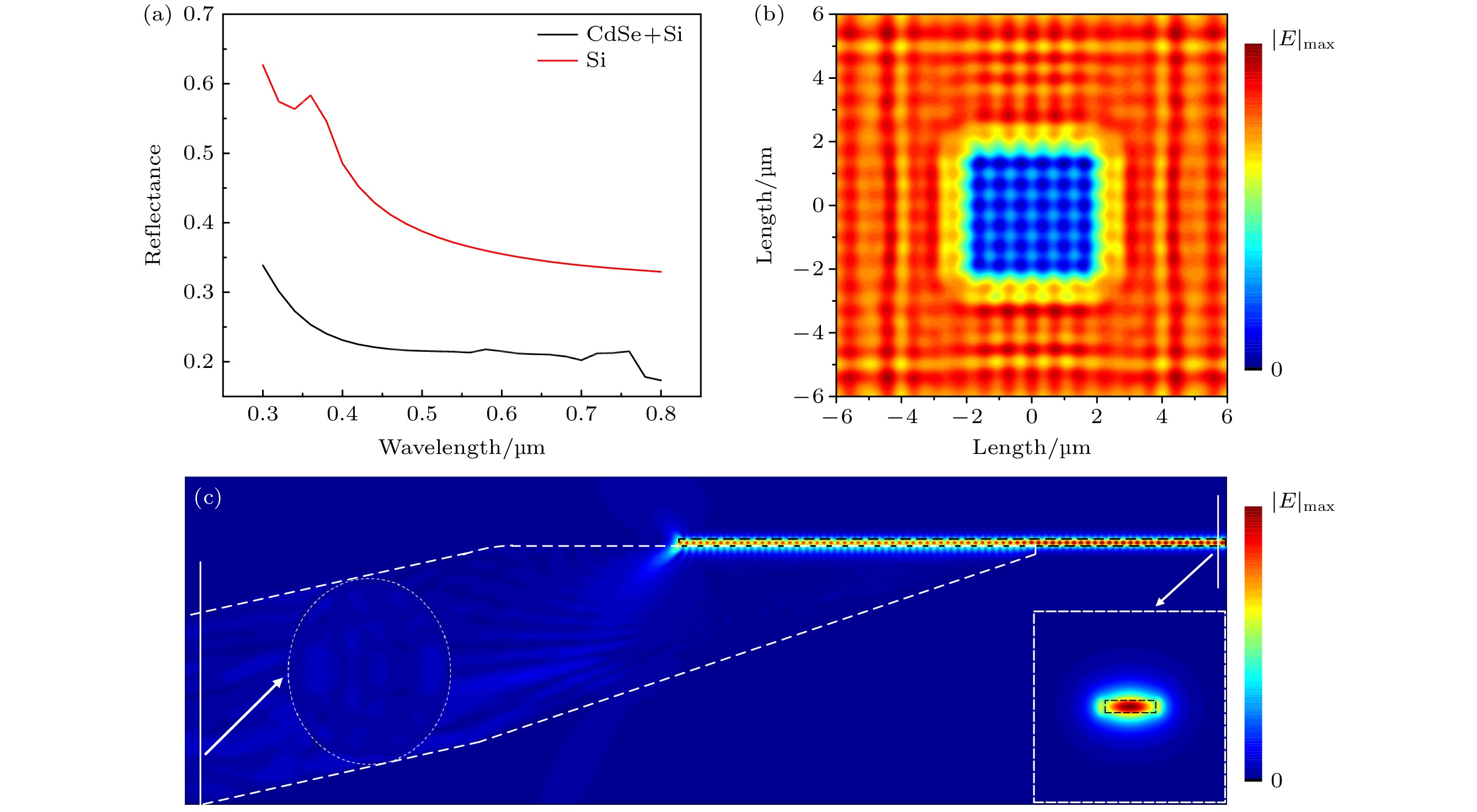
图 2 纳米线/锥形微光纤探针结构的光场模型 (a) 硅基底和硒化镉-硅基底的反射率; (b) 距样品表面 300 nm处的水平面的光场分布; (c) 纳米线/锥形微光纤探针结构倏逝场耦合(右侧插图为右侧白色实线处纳米线截面的TE模光场分布, 左侧圆形插图为左侧实线处锥形微光纤探针截面光场分布)
Figure 2. Optical field model of nanowire/tapered microfiber structure: (a) Reflectance of silicon substrate and cadmium selenide-silicon substrate; (b) horizontal optical field distribution at 300 nm above the sample surface; (c) nanowire/ tapered microfiber structure evanescent field coupling (The right inset is the TE mode optical field distribution of the nanowire cross section at the solid white line on the right, and the left circular inset is the optical field distribution of the tapered microfiber cross section at the solid line on the left).

图 3 扫描步长和探针-样品间距对系统成像质量的影响 (a) 不同扫描步长条件下的扫描结果; (b) 不同探针-样品间距条件下的扫描结果
Figure 3. Influence of scanning step length and probe-sample distance on the image quality: (a) Scan results under different scan steps; (b) scan results under different probe-sample distances.

图 4 不同样品的光学显微图和AFM扫描形貌图 (a), (b) 分别为S1的光学显微图和AFM扫描形貌图; (c), (d)分别为S2的光学显微图和AFM扫描形貌图; (e), (f)分别为S3的光学显微图和AFM扫描形貌图
Figure 4. Optical microscope and AFM scanning morphology image of the three samples: (a), (b) Optical microscope image and AFM topography of S1; (c), (d) optical microscope image and AFM topography of S2; (e), (f) optical microscope image and AFM topography of S3.
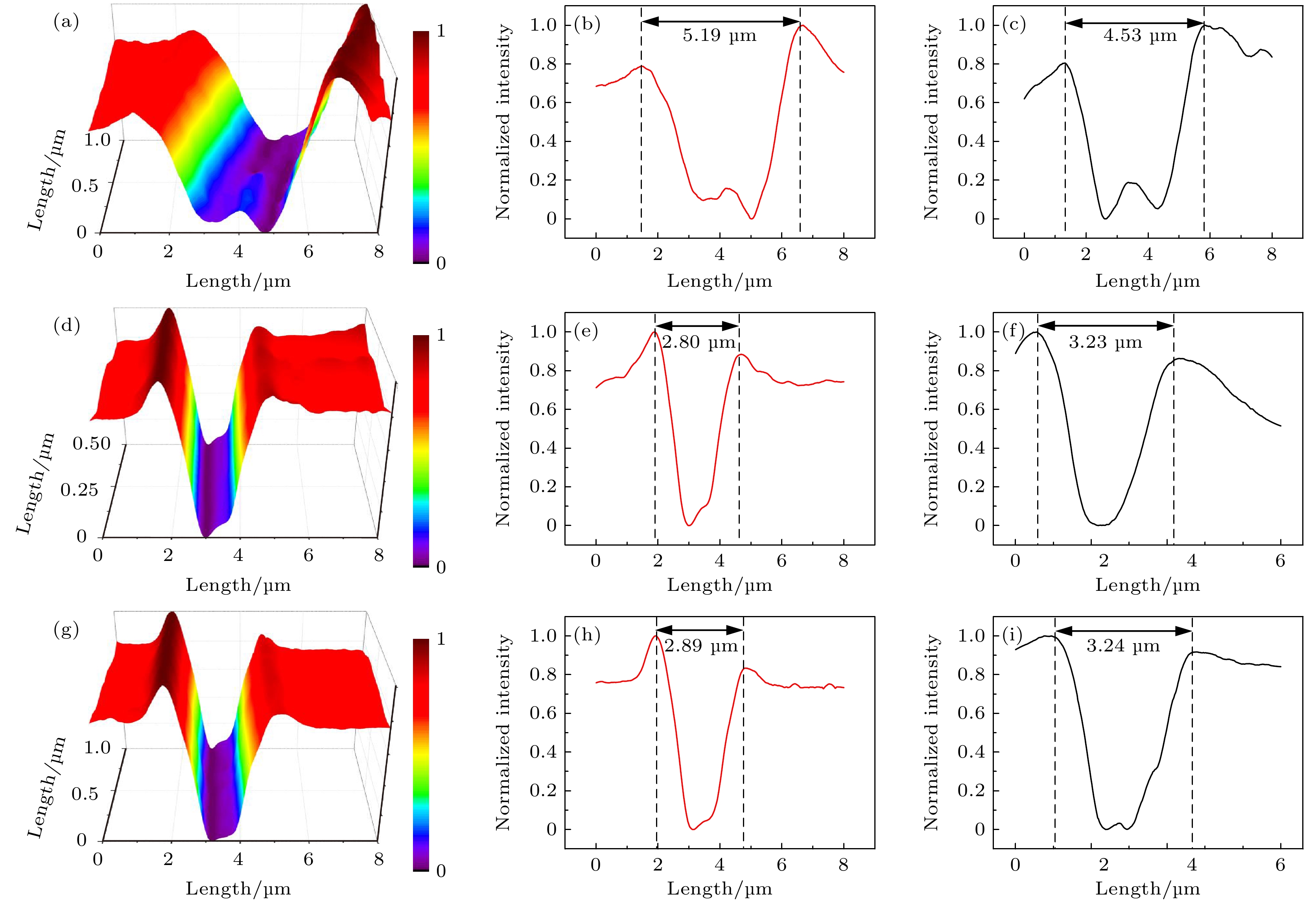
图 5 夹角θ = 23°时, 纳米线/锥形微光纤探针与传统锥形光纤探针对S1—S3样品的宽度测量值 (a), (d), (g) 分别为纳米线/锥形微光纤探针对S1—S3样品扫描的成像图; (b), (e), (h)分别为对应样品宽度的归一化测量结果; (c), (f), (i)同样条件下, 锥形光纤探针对S1—S3样品宽度的归一化测量结果
Figure 5. The width measurement results of S1–S3 samples with the nanowire/tapered microfiber probe and traditional tapered microfiber probe at θ = 23°: (a), (d), (g) Imaging results of the samples S1–S3 scanned by the nanowire/tapered microfiber probe; (b), (e), (h) measurement results of the width of the samples S1–S3 by the nanowire/tapered microfiber probe; (c), (f), (i) measurement results of the width of the samples S1–S3 by tapered microfiber probe.
表 1 CdS纳米线/锥形微光纤探针与传统锥形光纤探针测量结果对比
Table 1. Comparison of measurement results between CdS nanowire/tapered microfiber probe and traditional tapered microfiber probe.
样品 AFM/
μm锥形光纤探针 CdS纳米线/锥形光纤探针 θ = 23° θ = 23° θ = 38° 测量结果/μm 误差 测量结果/μm 误差 测量结果/μm 误差 S1 5.58 4.53 18.82% 5.19 6.99% 4.78 14.33% S2 2.61 3.23 23.75% 2.80 7.28% 2.99 14.56% S3 2.76 3.24 17.40% 2.89 4.71% 3.94 42.75%  DownLoad: CSV
-
[1] Trautman J K, Macklin J J, Brus L E, Betzig E 1994 Nature 369 40
Google Scholar
[2] Betzig E, Trautman J K 1992 Science 257 189
Google Scholar
[3] Ruckstuhl T, Verdes D, Winterflood C M, Seeger S 2011 Opt. Express 19 6836
Google Scholar
[4] 胡睿璇, 潘冰洋. 杨玉龙, 张伟华 2017 物理学报 66 144209
Google Scholar
Hu R X, Pan B Y, Yang Y L, Zhang W H 2017 Acta. Phys. Sin. 66 144209
Google Scholar
[5] Rayleigh L 1896 On the Theory of Optical Images, with Special Reference to the Microscope (Cambridge: Cambridge University Press) p167
[6] Betzig E, Trautman J K, Harris T D, Weiner J S, Kostelak R L 1991 Science 251 1468
Google Scholar
[7] Hermann R J, Gordon M J 2018 Annu. Rev. Chem. Biomol. 9 365
Google Scholar
[8] Novotny L, Stranick J S 2006 Annu. Rev. Phys. Chem. 57 303
Google Scholar
[9] Kalkbrenner T, Ramstein M, Mlynek J, Sandoghdar V 2001 J. Microsc. 202 72
Google Scholar
[10] Bharadwaj P, Novotny L 2007 Opt. Express 15 14266
Google Scholar
[11] Kim Z H, Leone S R 2006 J. Phys. Chem. B 110 19804
Google Scholar
[12] Sun L, Bai B, Meng X, Cui T, Shang G, Wang J 2018 Opt. Express 26 24637
Google Scholar
[13] Novotny L, Hulst N V 2011 Nat. Photonics 5 83
Google Scholar
[14] Palomba S, Novotny L 2009 Nano Lett. 9 3801
Google Scholar
[15] Hoeppener C, Lapin Z J, Bharadwaj P, Novotny L 2012 Phys. Rev. Lett. 109 017402
Google Scholar
[16] Pan B, Yang Y, Bian J, Hu X, Zhang W 2019 Opt. Commun. 445 273
Google Scholar
[17] Wei B, Melli M, Caselli N, et al. 2012 Science 338 1317
Google Scholar
[18] 伍晓芹, 王依霈, 童利民 2015 物理 44 356
Google Scholar
Wu X Q, Wang Y P, Tong L M 2015 Physics 44 356
Google Scholar
[19] 谷付星 2012 博士学位论文 (杭州: 浙江大学)
Gu F X 2012 Ph. D. Dissertation (Hangzhou: Zhejiang University) (in Chinese)
[20] Kim S, Yu N, Ma X, Zhu Y Z, Liu Q S, Liu M, Yan R X 2019 Nat. Photonics 13 636
Google Scholar
[21] Wu Y K, Liu X J, Qi X Z, Lu L, Guo G P, Guo G C, Ren X F 2021 Appl. Phys. Lett. 118 104002
Google Scholar
[22] Huang K, Yang S Tong L 2007 Appl. Opt. 46 1429
Google Scholar
[23] Marcatili E 1986 IEEE J. Quantum Electron. 22 988
Google Scholar
[24] Liao F, Wang Y, Peng T, Peng J, Gu Z Q, Yu H K, Chen T, Yu J X, Gu F X 2018 Adv. Opt. Mater. 6 1701012
Google Scholar
[25] Linghu S Y, Gu Z Q, Lu J S, et al. 2021 Nat. Commun. 12 385
[26] 王国军, 吴世法, 李旭峰, 李睿, 段建民, 潘石 2010 物理学报 59 192
Google Scholar
Wang G J, Wu S F, Li X F, Li R, Duan J M, Pan S 2010 Acta. Phys. Sin. 59 192
Google Scholar
[27] Zhang M Q, Wang J, Tian Q 2013 Chin. Phys. B 22 044202
Google Scholar
[28] 王佳, 武晓宇, 孙琳, 周炳琨 2016 扫描近场光学显微镜和纳米光学测量 (北京: 科学出版社) 第167, 247页
Wang J, Wu X Y, Sun L, Zhou B K 2016 Scanning Near-Field Optical Microscope and Nano-Optical Measurement (Beijing: Science Press) pp167, 247 (in Chinese)
[29] 石顺祥, 王学恩, 马琳 2014 物理光学与应用光学 (西安: 西安电子科技大学出版社) 第31, 77页
Shi S X, Wang X E, Ma L 2014 Physical Optics and Applied Optics (Xi’an: Xidian University Press) pp31, 77 (in Chinese)
[30] Yu J X, Liu F, Gu Z Q, Gu F X, Zhuang S L 2018 Opt. Express 26 6880
Google Scholar

 DownLoad:
Catalog
Metrics
- Abstract views: 4167
- PDF Downloads: 107
- Cited By: 0
