


-
The location and transmission of light is the core of modern photonic integrated device, and the proposal of topological photonics provides a new way of implementing optical manipulation. Topological photonic structures based on the quantum spin hall effect or quantum valley hall effect have the properties of immunity to defects and suppress backscattering, so they play a key role in designing novel low-loss photonic devices. In this work, we design a two-dimensional dielectric photonic crystal with time-reversal symmetry to achieve the coexistence of the quantum spin hall effect and the quantum valley hall effect in a photonic crystal. The design can be likened to an electronic system in which two pairs of Kramers simplex pairs are constructed to achieve a quadruple simplex pair in a photonic crystal. First, based on the method of shrinking and expanding the silicon pillars arranged in the honeycomb structure, the quadruple degeneracy point at the Γ point of the first Brillouin zone is opened, and the corresponding topologically trivial or non-trivial photonic band gap is formed,thereby realizing quantum spin hall effect. The expanded honeycomb lattice evolves into a Kagome structure, and then positive and negative perturbations are added to the Kagome lattice, breaking the spatial inversion symmetry of the Photonic crystal. When mirror symmetry is broken, different chiral photonic crystals can be created,leading the degeneracy point of the non-equivalent valleys K and K' in the Brillouin zone to be opened and a complete band gap to appear, thus realizing the Quantum valley hall effect. In the common band gap, topologically protected edge states are induced by nontrivial valley Chern number at the interface between two photonic crystals with opposite chirality. The numerical calculations show that unidirectional transport and bending-immune topological boundary states can be realized at the interface composed of topologically trivial (non-trivial) and positively (negatively) perturbed photonic crystals. Finally, a four-channel system based on the coexistence of the two effects is designed, The system is a novel electromagnetic wave router that can be selectively controlled by pseudospin degree of freedom or valley degree of freedom. This system provides a potential method for realizing the optical encoding and robust signal transmission, thereby providing greater flexibility for manipulating electromagnetic waves.
-
Keywords:
- photonic crystal /
- pseudospin /
- valley hall effect /
- topological phase transition
[1] Klitzing V K 2017 Annu. Rev. Conden. Ma. P. 8 13
 Google Scholar
[2] Qi X L, Zhang S C 2011 Rev. Mod. Phys. 83 1057
Google Scholar
[3] Haldane F D, Raghu S 2008 Phys. Rev. Lett. 100 013904
Google Scholar
[4] Wang Z, Chong Y D, Joannopoulos J D, Soljačić M 2009 Nature 461 772
Google Scholar
[5] 沈清玮 徐林 蒋建华 2017 物理学报 66 224102
Google Scholar
Shen Q W, Xu L, Jiang J H 2017 Acta Phys. Sin. 66 224102
Google Scholar
[6] Khanikaev A B, Hossein Mousavi S, Tse W K, Kargarian M, MacDonald A H, Shvets G 2013 Nat. Mater. 12 233
Google Scholar
[7] Chen W J, Jiang S J, Chen X D, Zhu B, Zhou L, Dong J W, Chan C T 2014 Nat. Commun. 5 1
[8] He C, Sun X C, Liu X P, Lu M H, Chen Y, Feng L, Chen Y F 2016 Proc. Natl. Acad. Sci. U. S. A. 113 4924
Google Scholar
[9] Hafezi M, Demler E A, Lukin M D, Taylor J M 2011 Nat. Phys. 7 907
Google Scholar
[10] Hafezi M, Mittal S, Fan J, Migdall A, Taylor J M 2013 Nat. Photonics 7 1001
Google Scholar
[11] Chen W J, Jiang S J, Chen X D, Zhu B, Zhou L, Dong J W, Chan C T 2014 Nat. Commun. 5 5782
Google Scholar
[12] Liang G Q, Chong Y D 2013 Phys. Rev. Lett. 110 203904
Google Scholar
[13] Ma T, Khanikaev A B, Mousavi S H, Shvets G 2015 Phys. Rev. Lett. 114 127401
Google Scholar
[14] Wu L H, Hu X 2015 Phys. Rev. Lett. 114 223901
Google Scholar
[15] Barik S, Miyake H, DeGottardi W, Waks E, Hafezi M 2016 New J. Phys. 18 113013
Google Scholar
[16] Anderson P D, Subramania G 2017 Opt. Express 25 23293
Google Scholar
[17] Zhang Z, Wei Q, Cheng Y, Zhang T, Wu D, Liu X 2017 Phys. Rev. Lett. 118 084303
Google Scholar
[18] Xia B Z, Liu T T, Huang G L, Dai H Q, Jiao J R, Zang X G, Liu J 2017 Phys. Rev. B 96 094106
Google Scholar
[19] Zhu X, Wang H X, Xu C, Lai Y, Jiang J H, John S 2018 Phys. Rev. B 97 085148
Google Scholar
[20] Chen M L, Jiang L J, Lan Z H, Sha W 2019 IEEE. Trans. Antennas Propag. 68 609
[21] 方云团, 王张鑫, 范尔盼, 李小雪, 王洪金 2020 物理学报 69 184101
Google Scholar
Fang Y T, Wang Z X, Fan E P, Li X X, Wang H J 2020 Acta Phys. Sin. 69 184101
Google Scholar
[22] 王彦兰, 李妍 2020 物理学报 69 094206
Google Scholar
Wang Y L, Li Y 2020 Acta Phys. Sin. 69 094206
Google Scholar
[23] Peng S, Schilder N J, Ni X, Van De Groep J, Brongersma M L, Alù A, Polman A 2019 Phys. Rev. Lett. 122 117401
Google Scholar
[24] Xie B, Su G, Wang H F, Liu F, Hu L, Yu S Y, Chen Y F 2020 Nat. Commun. 11 1
Google Scholar
[25] Ma T, Shvets G 2016 New J. Phys. 18 025012
Google Scholar
[26] Chen X D, Zhao F L, Chen M, Dong J W 2017 Phys. Rev. B 96 020202
Google Scholar
[27] Wiltshaw R, Craster R V, Makwana M P 2020 Wave Motion 99 102662
Google Scholar
[28] Wong S, Saba M, Hess O, Oh S S 2020 Phys. Rev. Res. 2 012011
Google Scholar
[29] Zhang L 2019 arXiv: 1903.03338 [physics. optics]
[30] Gong Y, Wong S, Bennett A J, Huffaker D L, Oh S S 2020 Acs. Photonics 7 2089
Google Scholar
[31] He X T, Liang E T, Yuan J J, Qiu H Y, Chen X D, Zhao F L, Dong J W 2019 Nat. Commun. 10 1
Google Scholar
[32] Han Y, Fei H, Lin H, Zhang Y, Zhang M, Yang Y 2021 Opt. Commun. 488 126847
Google Scholar
[33] Liu X L, Zhao L J, Zhang D, Gao S H 2022 Opt. Express 30 4965
Google Scholar
[34] Zhong H, Li Y D, Song D H, Kartashov Y V, Zhang Y Q 2020 Laser Photonics Rev. 14 7
[35] Zhong H, Xia S Q, Zhang Y Q, Li Y D, Song D H, Liu C L, Chen Z G 2021 Adv. Photonics 3 056001
[36] Tang Q, Zhang Y Q, V. Kartashov Y, Li Y D, V. Konotop V 2022 Chaos Solitons Fractals 161 112364
Google Scholar
[37] Tang Q, Ren B Q, Belić M R, Zhang Y Q, Li Y D 2022 Rom. Rep. Phys. 74 405
[38] Ren B Q, Wang H G, O. Kompanets V, V. Kartashov Y, Li Y D, Zhang Y Q 2021 Nanophoton. 10 3559
Google Scholar
[39] Arora S, Bauer T, Barczyk R, Verhagen E, Kuipers L 2021 Light Sci. Appl. 10 1
Google Scholar
[40] Chen M L, Jiang L J, Lan Z H, Sha W 2020 Phys. Rev. Res. 2 043148
Google Scholar
[41] Wei G C, Liu Z Z, Wang L C, Song J Y, Xiao J J 2022 Photonics Res. 10 999
Google Scholar
[42] Wu L H, Hu X 2016 Sci. Rep. 6 1
Google Scholar
[43] Liu F, Deng H Y, Wakabayashi K 2019 Phys. Rev. Lett. 122 086804
Google Scholar
[44] Wang C, Zhang H, Yuan H, Zhong J, Lu C 2020 Front. Optoelectron. 13 73
Google Scholar
[45] Oh S S, Lang B, Beggs D M, Huffaker D L, Saba M, Hess O 2018 The 13th Pacific Rim Conference on Lasers and Electro-Optics Hongkong, China, July 29–August 3, 2018 pTh4H5
-
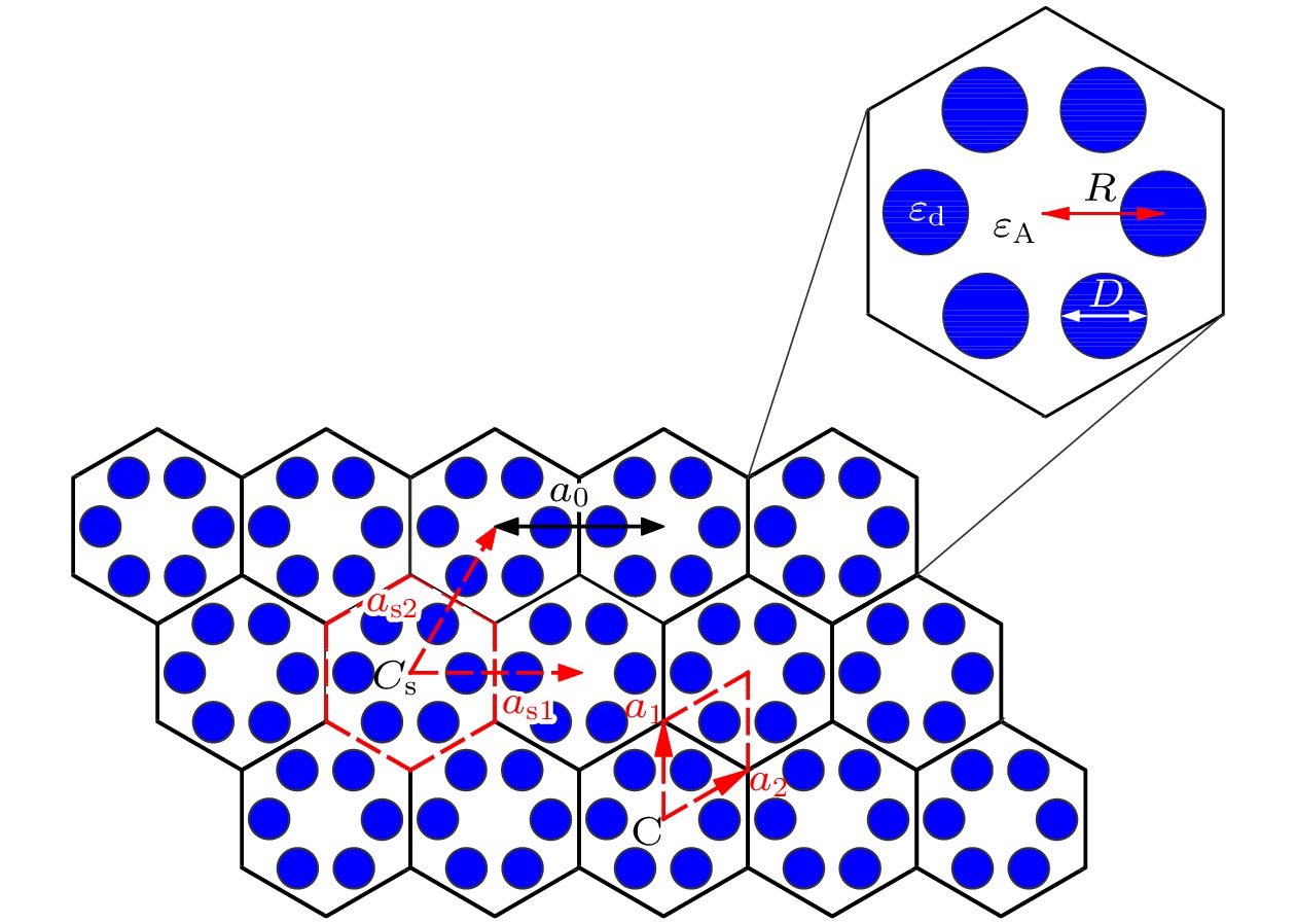
图 1 PC示意图, 红色向量分别表示六边形和菱形原胞的单位向量, 长度
$ {a}_{0} $ 是晶格常数. 右图为六边形单胞的放大图, R为相邻硅柱间距, D为硅柱的直径,$ {\varepsilon }_{{\rm{d}}}{\rm{和}}{\varepsilon }_{{\rm{A}}} $ 分别是硅和周围环境的介电常数Figure 1. PC schematic diagram, red vectors represent unit vectors of hexagonal and rhomboid unit cell respectively, and the length of lattice constant is
$ {a}_{0} $ . The right figure is an enlarged view of a hexagonal cell. R is the distance between adjacent silicon columns and D is the diameter of cylinder.$ {\varepsilon }_{{\rm{d}}}, {\varepsilon }_{{\rm{A}}} $ are dielectric constants of cylinder and surrounding environment, respectively.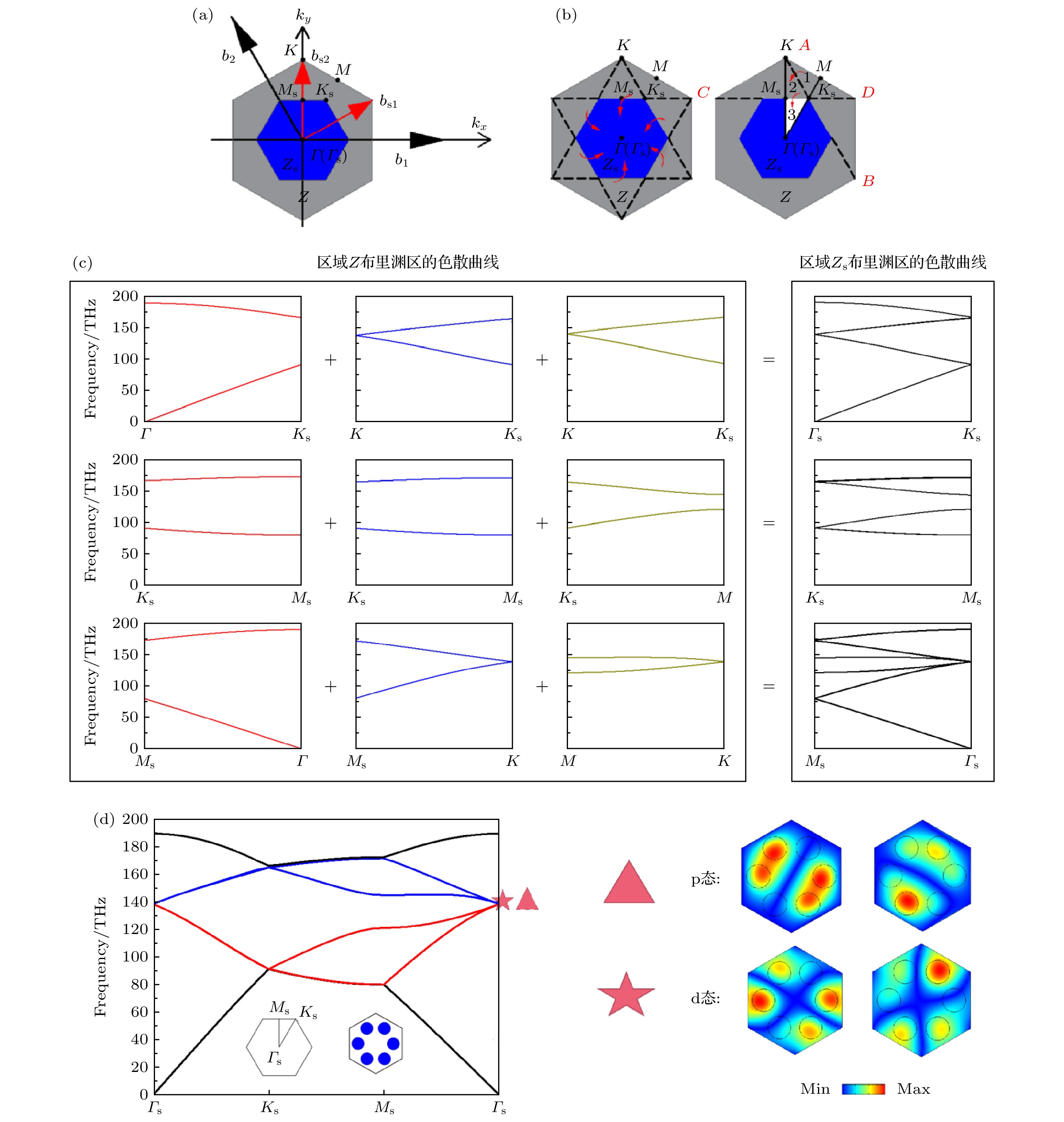
图 2 (a)灰色区域表示菱形原胞的BZ, 用
$ Z $ 表示, 蓝色区域表示六边形原胞的BZ, 用$ {Z}_{{\rm{s}}} $ 表示, ($ {b}_{1}, {b}_{2} $ )和($ {b}_{{\rm{s}}1}, {b}_{{\rm{s}}2} $ )是对应的倒格子基矢; (b)从$ Z $ 到$ {Z}_{{\rm{s}}} $ 的折叠机制示意图; (c)菱形原胞的BZ内选择不同的扫描路径的能带色散图及折叠到六边形原胞的BZ内的能带色散图; (d)基于单胞$ {C}_{{\rm{s}}} $ 的色散曲线, 插图为原始单胞和扫描的BZ, 结构参数为${a}_{0}=1~{\rm{μ }}{\rm{m}}$ ,$D=0.24 {a}_{0}$ ,$ R/{a}_{0}=1/3 $ , 右图为狄拉克四重简并点的电场图Figure 2. (a) The gray area denoted by
$ Z $ represents the BZ of the rhomboid unit cell; the blue area denoted by$ {Z}_{{\rm{s}}} $ represents the BZ of the hexagonal unit cell; ($ {b}_{1}, {b}_{2} $ ) and ($ {b}_{{\rm{s}}1}, {b}_{{\rm{s}}2} $ ) are the corresponding inverted lattice basis vectors, respectively; (b) the folding mechanism from$ Z $ to$ {Z}_{{\rm{s}}} $ ; (c) band dispersion maps in the BZ of the rhomboid unit cell with different scanning paths, and band dispersion maps with different scanning paths based on the folding mechanism; (d) dispersion curves based on a single cell$ {C}_{{\rm{s}}} $ , and the inset is the original single cell and the scanned BZ, the structural parameters are${a}_{0}=1~{\rm{μ }}{\rm{m}}$ ,$D=0.24 {a}_{0}$ ,$ R/{a}_{0}=1/3 $ , the right of Fig. (d) is electric fields of Dirac quadruple degenerate points.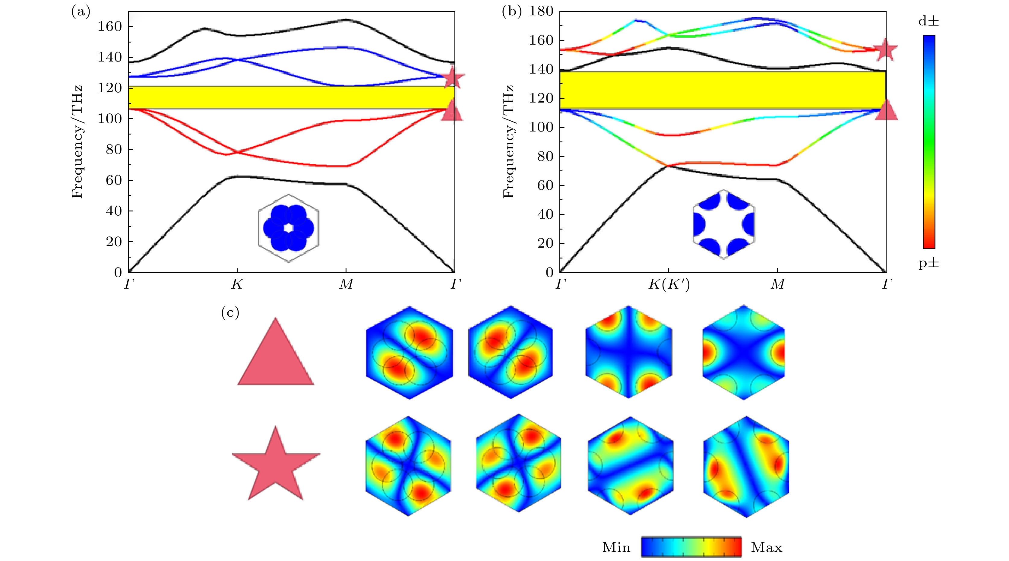
图 3
$ R/{a}_{0}=0.25 $ ($D=0.36 {a}_{0}$ ) (a)和$ R/{a}_{0}=0.5 $ ($D=0.4 {a}_{0}$ )(b)的能带图, 说明$ \varGamma $ 发生p, d模式反转(b); (c)晶格结构为$ R/{a}_{0}=0.25 $ 时上下能级的电场图(左1和左2)和晶格结构为$ R/{a}_{0}=0.5 $ 时上下能级的电场图(右1和右2)Figure 3. Energy bands of lattices with
$ R/{a}_{0}=0.25 $ ($D=0.36 {a}_{0}$ )(a) and$ R/{a}_{0}=0.5 $ ($D=0.4 {a}_{0}$ )(b), respectively, the p and d modes reversal occurs in$ \varGamma $ (b); (c) two columns on the left: electric fields of the p or d state at point Γ for the lattice with$R/{a}_{0}=0.25\left({\rm{l}}{\rm{e}}{\rm{f}}{\rm{t}}\; 1\;{\rm{ }}{\rm{a}}{\rm{n}}{\rm{d}}\;2\right)$ , two columns on the right: electric fields for the p or d state for the lattice with$R/{a}_{0}=0.5\left({\rm{r}}{\rm{i}}{\rm{g}}{\rm{h}}{\rm{t}}{\rm{ }}\;1\;{\rm{ }}{\rm{a}}{\rm{n}}{\rm{d}}\; 2\right)$ 
图 4 (a)KPC的结构示意图; (b)
$D=0.4 {a}_{0}, R/{a}_{0}=0.5, d=1.2 {d}_{0}$ 或$d=0.8 {d}_{0}~({d}_{0}=\dfrac{{a}_{0}}{2 \sqrt{3}})$ 的KPC的色散曲线; (c)第一、二条能带$K\left({K}'\right)$ 点的相位图及上下能带$ \varGamma $ 点的电场图; (d)KPC原胞正扰动和负扰动第一条能带的Berry曲率Figure 4. (a) The structure diagram of KPC; (b) the dispersion curve of KPC with
$D=0.4 {a}_{0}$ ,$ R/{a}_{0}=0.5 $ ,$d=1.2 {d}_{0}$ or$d=0.8 {d}_{0} $ $ \Big({d}_{0}=\dfrac{{a}_{0}}{2\sqrt{3}}\Big)$ ; (c) phase diagram of the first and second band$K\left({K}'\right)$ and electric field diagram of the upper and lower band$ \varGamma $ ; (d) Berry curvature of the first band of positive or negative perturbations of the KPC unit cell.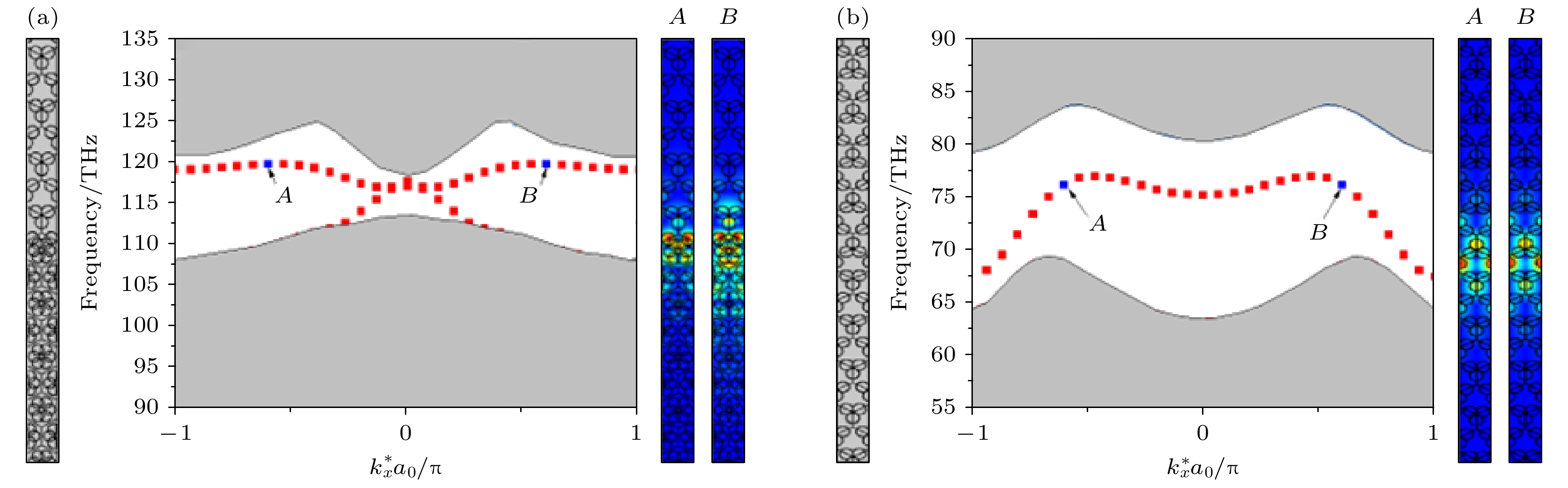
图 5 (a)赝自旋极化边缘态, 拓扑平凡PC和拓扑非平凡PC组成超胞的几何结构、能带结构以及A, B两点对应的电场分布图;(b)谷极化边缘态, 由正扰动和负扰动KPC结构所组成的几何结构、能带结构以及A, B两点对应的电场分布图
Figure 5. (a) Pseudospin-polarized edge states, the structure and the energy band of a supercell composed of the topological trivial PC and the topological nontrivial PC, and the electric field distribution corresponding to points A and B at the energy band; (b) valley-polarized edge states, the geometry and band structure of the KPC consisting of positive and negative perturbations and the corresponding electric field distribution at points A and B.
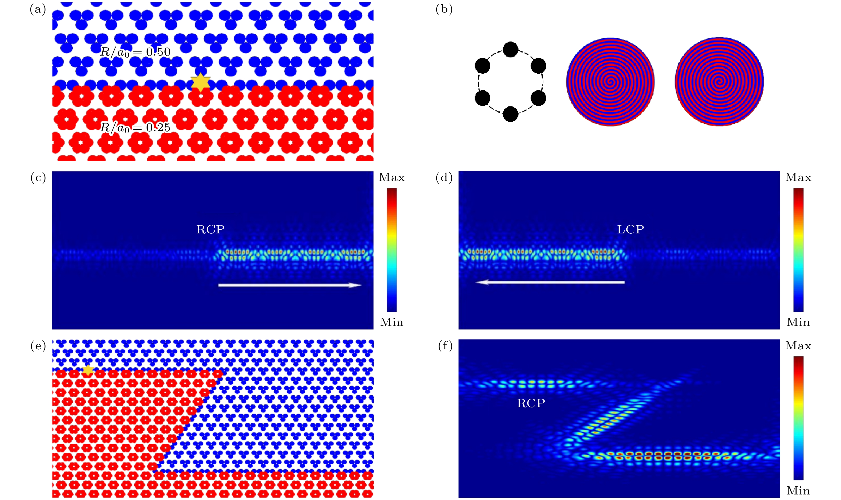
图 6 赝自旋边缘态的光传输特性和场分布(a)由
$ R=0.5*{a}_{0} $ (蓝色区域)非平凡结构和$ R=0.25*{a}_{0} $ 平凡结构(红色区域)组成直波导示意图, 图中黄色的六角形表示手性源的位置; (b)6个点源组成的手性激发源示意图, 相邻点源的相位差是$ {\text{π}}/3 $ ; (c)和(d)直波导中分别由RCP和LCP光源所激发的光束电场强度分布; (e)由$ R=0.5*{a}_{0} $ (蓝色区域)和$ R=0.25*{a}_{0} $ (红色区域)组成的“Z”字形波导; (f)Z字形波导中RCP源所激发的电场分布图Figure 6. Optical transmission characteristics and the electric field distribution of the pseudospin boundary state: (a) Schematic diagram of the straight waveguide consisting of the non-trivial structure with
$ R=0.5*{a}_{0} $ (blue area) and the trivial structure with$ R=0.25*{a}_{0} $ (red area), the yellow hexagon in the diagram shows the position of the excitation source; (b) schematic diagram of a chiral power consisting of six antennas, and the phase difference between adjacent antennas is π/3; (c), (d) the electric field intensity distributions excited by RCP or LCP sources, respectively; (e) Z-shaped waveguide consisting of$ R=0.5*{a}_{0} $ (blue area) and$ R=0.25*{a}_{0} $ (red area); (f) field intensity distribution of the electric field excited by the RCP source.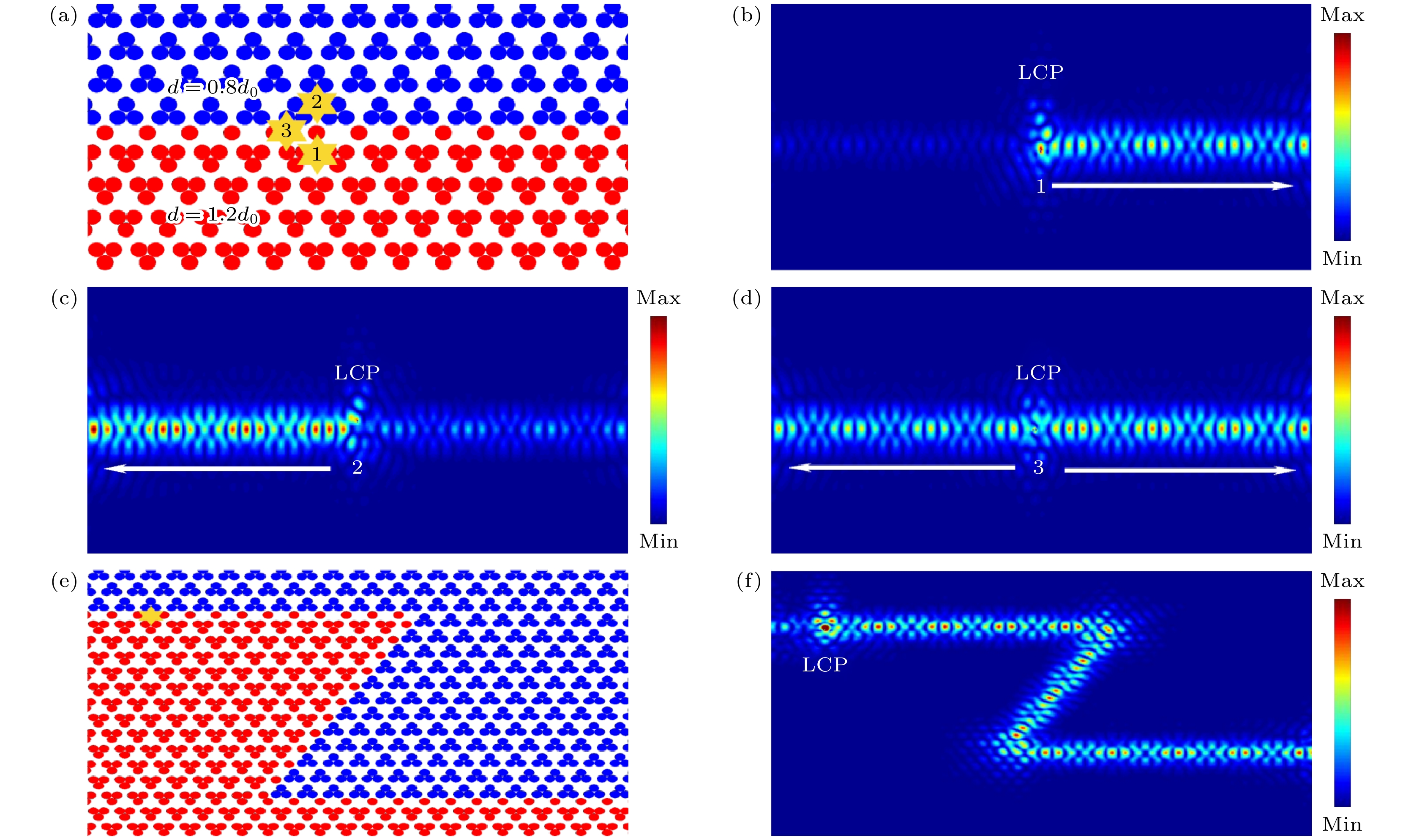
图 7 谷边缘态的光传输特性和场分布(a)由
$d = 0.8{d}_{0}$ (蓝色区域)和$d = 1.2{d}_{0}$ (红色区域)组成的直波导示意图, 左手性源(标记为六角形)放置在正扰动和负扰动KPC界面附近的不同位置处, 以激发不同的边缘模式; (b)—(d)分别由LCP光源在不同的激发源位置所激发的光束电场强度分布; (e)和(f)分别是构建的“Z”字形拓扑波导, 以及由黄星表示的LCP源所激发的电场强度分布Figure 7. Optical transmission characteristics and the electric field distribution of the valley edge state: (a) Schematic diagram of valley waveguide composed of
$d=0.8 {d}_{0}$ (blue region) and$d=1.2 {d}_{0}$ (red region), the left-handed circular polarized dipoles (marked as the hexagon) placed at different locations near the interface between KPCs with positive or negative disturbances to excite edge modes; (b)–(d) are the electric field intensity distributions excited by the LCP light source at different positions; (e) schemes of z-shaped waveguide; (f) the electric field intensity distribution of Z-shaped waveguide excited by the LCP source.
图 8 (a)四通道系统的结构图; (b)谷激发的场强分布; (c)赝自旋激发的场强分布
Figure 8. (a)The four-channel system for the electromagnetic wave routing; (b) the field intensity distribution of the valley excitation; (c) the field intensity distribution of the pseudospin excitation.
-
[1] Klitzing V K 2017 Annu. Rev. Conden. Ma. P. 8 13
Google Scholar
[2] Qi X L, Zhang S C 2011 Rev. Mod. Phys. 83 1057
Google Scholar
[3] Haldane F D, Raghu S 2008 Phys. Rev. Lett. 100 013904
Google Scholar
[4] Wang Z, Chong Y D, Joannopoulos J D, Soljačić M 2009 Nature 461 772
Google Scholar
[5] 沈清玮 徐林 蒋建华 2017 物理学报 66 224102
Google Scholar
Shen Q W, Xu L, Jiang J H 2017 Acta Phys. Sin. 66 224102
Google Scholar
[6] Khanikaev A B, Hossein Mousavi S, Tse W K, Kargarian M, MacDonald A H, Shvets G 2013 Nat. Mater. 12 233
Google Scholar
[7] Chen W J, Jiang S J, Chen X D, Zhu B, Zhou L, Dong J W, Chan C T 2014 Nat. Commun. 5 1
[8] He C, Sun X C, Liu X P, Lu M H, Chen Y, Feng L, Chen Y F 2016 Proc. Natl. Acad. Sci. U. S. A. 113 4924
Google Scholar
[9] Hafezi M, Demler E A, Lukin M D, Taylor J M 2011 Nat. Phys. 7 907
Google Scholar
[10] Hafezi M, Mittal S, Fan J, Migdall A, Taylor J M 2013 Nat. Photonics 7 1001
Google Scholar
[11] Chen W J, Jiang S J, Chen X D, Zhu B, Zhou L, Dong J W, Chan C T 2014 Nat. Commun. 5 5782
Google Scholar
[12] Liang G Q, Chong Y D 2013 Phys. Rev. Lett. 110 203904
Google Scholar
[13] Ma T, Khanikaev A B, Mousavi S H, Shvets G 2015 Phys. Rev. Lett. 114 127401
Google Scholar
[14] Wu L H, Hu X 2015 Phys. Rev. Lett. 114 223901
Google Scholar
[15] Barik S, Miyake H, DeGottardi W, Waks E, Hafezi M 2016 New J. Phys. 18 113013
Google Scholar
[16] Anderson P D, Subramania G 2017 Opt. Express 25 23293
Google Scholar
[17] Zhang Z, Wei Q, Cheng Y, Zhang T, Wu D, Liu X 2017 Phys. Rev. Lett. 118 084303
Google Scholar
[18] Xia B Z, Liu T T, Huang G L, Dai H Q, Jiao J R, Zang X G, Liu J 2017 Phys. Rev. B 96 094106
Google Scholar
[19] Zhu X, Wang H X, Xu C, Lai Y, Jiang J H, John S 2018 Phys. Rev. B 97 085148
Google Scholar
[20] Chen M L, Jiang L J, Lan Z H, Sha W 2019 IEEE. Trans. Antennas Propag. 68 609
[21] 方云团, 王张鑫, 范尔盼, 李小雪, 王洪金 2020 物理学报 69 184101
Google Scholar
Fang Y T, Wang Z X, Fan E P, Li X X, Wang H J 2020 Acta Phys. Sin. 69 184101
Google Scholar
[22] 王彦兰, 李妍 2020 物理学报 69 094206
Google Scholar
Wang Y L, Li Y 2020 Acta Phys. Sin. 69 094206
Google Scholar
[23] Peng S, Schilder N J, Ni X, Van De Groep J, Brongersma M L, Alù A, Polman A 2019 Phys. Rev. Lett. 122 117401
Google Scholar
[24] Xie B, Su G, Wang H F, Liu F, Hu L, Yu S Y, Chen Y F 2020 Nat. Commun. 11 1
Google Scholar
[25] Ma T, Shvets G 2016 New J. Phys. 18 025012
Google Scholar
[26] Chen X D, Zhao F L, Chen M, Dong J W 2017 Phys. Rev. B 96 020202
Google Scholar
[27] Wiltshaw R, Craster R V, Makwana M P 2020 Wave Motion 99 102662
Google Scholar
[28] Wong S, Saba M, Hess O, Oh S S 2020 Phys. Rev. Res. 2 012011
Google Scholar
[29] Zhang L 2019 arXiv: 1903.03338 [physics. optics]
[30] Gong Y, Wong S, Bennett A J, Huffaker D L, Oh S S 2020 Acs. Photonics 7 2089
Google Scholar
[31] He X T, Liang E T, Yuan J J, Qiu H Y, Chen X D, Zhao F L, Dong J W 2019 Nat. Commun. 10 1
Google Scholar
[32] Han Y, Fei H, Lin H, Zhang Y, Zhang M, Yang Y 2021 Opt. Commun. 488 126847
Google Scholar
[33] Liu X L, Zhao L J, Zhang D, Gao S H 2022 Opt. Express 30 4965
Google Scholar
[34] Zhong H, Li Y D, Song D H, Kartashov Y V, Zhang Y Q 2020 Laser Photonics Rev. 14 7
[35] Zhong H, Xia S Q, Zhang Y Q, Li Y D, Song D H, Liu C L, Chen Z G 2021 Adv. Photonics 3 056001
[36] Tang Q, Zhang Y Q, V. Kartashov Y, Li Y D, V. Konotop V 2022 Chaos Solitons Fractals 161 112364
Google Scholar
[37] Tang Q, Ren B Q, Belić M R, Zhang Y Q, Li Y D 2022 Rom. Rep. Phys. 74 405
[38] Ren B Q, Wang H G, O. Kompanets V, V. Kartashov Y, Li Y D, Zhang Y Q 2021 Nanophoton. 10 3559
Google Scholar
[39] Arora S, Bauer T, Barczyk R, Verhagen E, Kuipers L 2021 Light Sci. Appl. 10 1
Google Scholar
[40] Chen M L, Jiang L J, Lan Z H, Sha W 2020 Phys. Rev. Res. 2 043148
Google Scholar
[41] Wei G C, Liu Z Z, Wang L C, Song J Y, Xiao J J 2022 Photonics Res. 10 999
Google Scholar
[42] Wu L H, Hu X 2016 Sci. Rep. 6 1
Google Scholar
[43] Liu F, Deng H Y, Wakabayashi K 2019 Phys. Rev. Lett. 122 086804
Google Scholar
[44] Wang C, Zhang H, Yuan H, Zhong J, Lu C 2020 Front. Optoelectron. 13 73
Google Scholar
[45] Oh S S, Lang B, Beggs D M, Huffaker D L, Saba M, Hess O 2018 The 13th Pacific Rim Conference on Lasers and Electro-Optics Hongkong, China, July 29–August 3, 2018 pTh4H5


 DownLoad:


Catalog
Metrics
- Abstract views: 2739
- PDF Downloads: 153
- Cited By: 0
