


-
Defect is one of the central issues in semiconductors. MoS2 is sensitive to irradiation and can be damaged by electron beams, accompanied with the generation of sulfur vacancies. However, the dynamics for the defect generation process is still unclear. In this work, we employ the time-dependent density functional theory to simulate the process of a sulfur atom sputtering from the MoS2, producing a sulfur vacancy defect in the lattice. We find that there exists a strong non-adiabatic effect in the process. During the formation of the sulfur vacancy, there exist electron transitions which can be described by the Landau-Zener model. As the sulfur atom leaves away from the lattice, two energy levels from the valence bands rise up and one energy level from the conduction band falls down. When the spin-orbit coupling (SOC) is not considered, those levels do not couple with each other. However, when the SOC is taken into account, electrons can transit between those levels. The transition probability is related to the kinetic energy of the sputtered sulfur atom. As the kinetic energy of the sulfur atom increases, the non-adiabatic electron transitions are enhanced. The evolution of the energy levels is also strongly dependent on the kinetic energy of the sputtered sulfur atom, which is induced by the non-adiabatic electron transition. It is worth noting that the SOC plays a key role in sputtering sulfur atoms, although the system produces no magnetic moments in the whole process. The non-adiabatic effect enhances the energy barrier of the sulfur sputtering. As the initial kinetic energy of the sputtered sulfur atom increases, the energy barrier increases, and exhibits a jump around the initial kinetic energy of ~22 eV, which can be explained by the non-adiabatic electron occupation and the Coulomb repulsion. Beside the energy barrier, the non-adiabatic effect also modifies the charge distribution. When the kinetic energy of the sputtered sulfur atom is relatively low, more electrons occupy the pz level; when the kinetic energy is relatively high, more electrons occupy the pxy level instead. The sputtered sulfur atom always carries a bit more electrons, leaving holes around the vacancy defect. Our work reveals the dynamics of the sulfur sputtering and vacancy formation in MoS2, particularly the non-adiabatic effect in the process. It builds the theoretical foundation for defect engineering. [1] Bozheyev F, Ellmer K 2022 J. Mater. Chem. A 10 9327
 Google Scholar
[2] Khatua D P, Singh A, Gurung S, Khan S, Tanwar M, Kumar R, Jayabalan J 2022 J. Phys. Condens. Matter. 34 155401
Google Scholar
[3] Ganatra R, Zhang Q 2014 ACS Nano 8 4074
Google Scholar
[4] Singh E, Singh P, Kim K S, Yeom G Y, Nalwa H S 2019 ACS Appl. Mater. Interfaces 11 11061
Google Scholar
[5] Nawz T, Safdar A, Hussain M, Sung Lee D, Siyar M 2020 Crystals 10 902
Google Scholar
[6] Sanikop R, Sudakar C 2019 ACS Appl. Nano Mater. 3 576
Google Scholar
[7] Islam M M, Dev D, Krishnaprasad A, Tetard L, Roy T 2020 Sci. Rep. 10 21870
Google Scholar
[8] Wu F, Tian H, Shen Y, Hou Z, Ren J, Gou G Y, Sun Y B, Yang Y, Ren T L 2022 Nature 603 259
Google Scholar
[9] Cao Y 2021 ACS Nano 15 11014
Google Scholar
[10] Zhao G Y, Deng H, Nathaniel T, Michael G, Abdellah L, Peng Q, Yan J A, Wang C D, Lan Y C 2019 Appl. Sci. 9 678
Google Scholar
[11] Pandey M, Rasmussen F A, Kuhar K, Olsen T, Jacobsen K W, Thygesen K S 2016 Nano Lett. 16 2234
Google Scholar
[12] Wang Y Q, Deng L J, Wei Q L, Wan Y, Liu Z, Lu X, Li Y, Bi L, Zhang L, Lu H P, Chen H Y, Zhou P H, Zhang L B, Cheng Y C, Zhao X X, Ye Y, Huang W, Pennycook S J, Loh K P, Peng B 2020 Nano Lett. 20 2129
Google Scholar
[13] Taffelli A, Dirè S, Quaranta A, Pancheri L 2021 Sensors 21 2758
Google Scholar
[14] Sorkin V, Zhou H, Yu Z G, Ang K W, Zhang Y W 2022 Sci. Rep. 12 18001
Google Scholar
[15] Wang Y, Liu S, Li Q, Quhe R, Yang C, Guo Y, Zhang X, Pan Y, Li J, Zhang H, Xu L, Shi B, Tang H, Li Y, Yang J, Zhang Z, Xiao L, Pan F, Lu J 2021 Rep. Prog. Phys. 84 056501
Google Scholar
[16] Cheng Y, Wan R, Li L, Liu Z, Yan S, Li L, Wang J, Gao Y 2022 J. Opt. 24 2040
Google Scholar
[17] Cheng Y, Song H, Wu H, Zhang P, Tang Z, Lu S 2020 Chem. Asian J. 15 3123
Google Scholar
[18] Xie Y, Liang F, Chi S, Wang D, Zhong K, Yu H, Zhang H, Chen Y, Wang J 2020 ACS Appl. Mater. Interfaces 12 7351
Google Scholar
[19] Yang Z, Zhu L, Lü C, Zhang R, Wang H, Wang J, Zhang Q 2021 Mater. Chem. Front. 5 5880
Google Scholar
[20] Komsa H P, Kotakoski J, Kurasch S, Lehtinen O, Kaiser U, Krasheninnikov A V 2012 Phys. Rev. Lett. 109 035503
Google Scholar
[21] Susi T, Meyer J C, Kotakoski J 2019 Nat. Rev. Phys. 1 397
Google Scholar
[22] Yoshimura A, Lamparski M, Kharche N, Meunier V 2018 Nanoscale 10 2388
Google Scholar
[23] Ugurlu O, Haus J, Gunawan A A, Thomas M G, Maheshwari S, Tsapatsis M, Mkhoyan K A 2011 Phys. Rev. B 83 113408
Google Scholar
[24] Lehnert T, Lehtinen O, Algara-Siller G, Kaiser U 2017 Appl. Phys. Lett. 110 033106
Google Scholar
[25] Tai K L, Huang C W, Cai R F, Huang G M, Tseng Y T, Chen J, Wu W W 2020 Small 16 1905516
Google Scholar
[26] Meyer J C, Eder F, Kurasch S, Skakalova V, Kotakoski J, Park H J, Roth S, Chuvilin A, Eyhusen S, Gred B, Krasheninnikov A V, Kaiser U 2012 Phys. Rev. Lett. 108 196102
Google Scholar
[27] Kretschmer S, Lehnert T, Kaiser U, Krasheninnikov A V 2020 Nano Lett. 20 2865
Google Scholar
[28] Runge E, Gross E K 1984 Phys. Rev. Lett. 52 997
Google Scholar
[29] Jia W, Fu J, Cao Z, Wang L, Chi X, Gao W, Wang L W 2013 J. Comput. Phys. 251 102
Google Scholar
[30] Jia W, Cao Z, Wang L, Fu J, Chi X, Gao W, Wang L W 2013 Comput. Phys. Commun. 184 9
Google Scholar
[31] Hamann D R, Schlüter M, Chiang C 1979 Phys. Rev. Lett. 43 1494
Google Scholar
[32] Hamann D R 2013 Phys. Rev. B 88 085117
Google Scholar
[33] Shen Y T, Xu T, Tan X D, He L B, Yin K B, Wan N, Sun L T 2018 Adv. Mater. 30 1705954
Google Scholar
[34] Zener C 1932 Proc. R. Soc. London, Ser. A 137 696
Google Scholar
[35] Olson A J, Wang S J, Niffenegger R J, Li C H, Greene C H, Chen Y P 2014 Phys. Rev. A 90 013616
Google Scholar
[36] Wang L W 2002 Phys. Rev. B 65 153410
Google Scholar
-
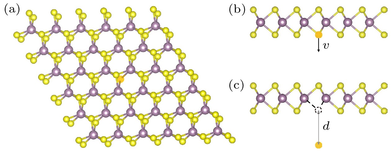
图 1 (a) 5 × 5的完整MoS2超胞; (b) 发生弹性碰撞后, S原子获得一定的初始速度v脱离晶格, 其速度方向垂直于晶格; (c) S原子脱离晶格后运动到距离晶格为d的位置. 图中黄色球与紫色球分别代表S原子与Mo原子, 高亮的原子为脱离晶格的S原子
Figure 1. (a) The 5 × 5 supercell of MoS2; (b) after the elastic collision with electrons, the S atom gets an initial velocity v, whose direction is perpendicular to the lattice; (c) the moving distance d of the S atom after sputtering from the lattice. Yellow and purple balls represent the sulfur and molybdenum atoms, respectively. The highlighted ball represents the sputtered S atom.

图 2 (a) 当S原子以不同初始动能脱离晶格时, 系统势能Ep随S原子运动距离d的变化关系, 其中初始时刻完整MoS2晶格的情况为势能零点; (b) S原子脱离晶格所需越过的能量势垒与初始动能的关系
Figure 2. (a) For the sulfur atom with various initial kinetic energies, the energy Ep as a function of the atom distance d, where the energy of the perfect MoS2 lattice is set to zero; (b) energy barriers for the S sputtering process as a function of the initial kinetic energy.

图 3 系统能级随S原子运动距离d的变化情况. 能级上的红色气泡表示该能级被电子占据, 气泡大小表示电子占据数. 插图为箭头所指能级的电荷分布 (a) 不考虑SOC; (b) 考虑SOC且脱离晶格的S原子的初始动能较低(Ek = 15.2 eV); (c) 考虑SOC且脱离晶格的S原子的初始动能较高(Ek = 30.4 eV)
Figure 3. Energy levels of the system as a function of the atom distance d. Red bubble on an energy level indicates that the energy level is occupied by electrons, and the size of the bubble indicates the number of electrons occupied. The insets show the charge densities of the corresponding states: (a) Without SOC; (b) with SOC and a low initial kinetic energy of the S atom (Ek = 15.2 eV); (c) with SOC and a high initial kinetic energy of the S atom (Ek = 30.4 eV).

图 4 (a) 当脱离晶格的S原子初始动能较低时(Ek = 15.2 eV), 相关能级上电子占据数的变化; (b) 当脱离晶格的S原子初始动能较高时(Ek = 30.4 eV), 相关能级上电子占据数的变化; (c) 原子运动距离d = 3 Å时, 高能量能级上的电子占据数随S原子初始动能
$ {E}_{{\rm{k}}} $ 的变化Figure 4. (a) When the initial kinetic energy of the sputtered S atom is low (Ek = 15.2 eV), the electron occupations on the relevant states as functions of the atom distance; (b) when the initial kinetic energy of the sputtered S atom is high (Ek = 30.4 eV), the electron occupations on the relevant states as functions of the atom distance; (c) electron occupation on the high-energy state as a function of the initial kinetic energy
$ {E}_{{\rm{k}}} $ of the sputtered S atom, when the atom distance d = 3 Å.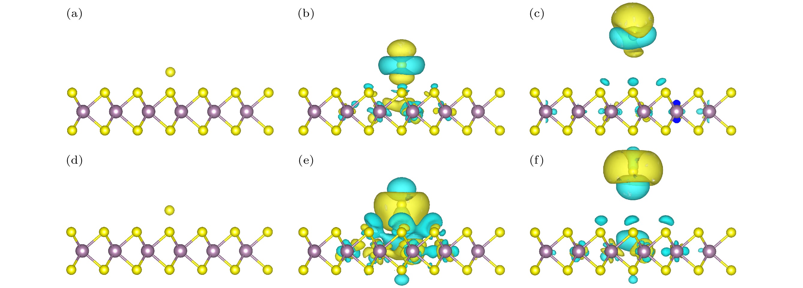
图 5 当脱离晶格原子的运动距离d取不同值时, 非绝热模拟与绝热模拟所得的电荷密度之差(蓝色和黄色等值面分别代表电荷的减少和增加) (a)—(c) 低速条件(Ek = 15.2 eV)下, (a) d = 1.75 Å, (b) d = 2.25 Å, (c) d = 5.00 Å; (d)—(f) 高速条件(Ek = 30.4 eV)下, (d) d = 1.75 Å, (e) d = 2.25 Å, (f) d = 5.00 Å
Figure 5. Charge density difference between the non-adiabatic and adiabatic results at different atom distances d (Blue and yellow isosurfaces represent the charge depletion and accumulation respectively): (a)–(c) When the initial kinetic energy of the sputtered S atom is low (Ek = 15.2 eV), (a) d = 1.75 Å, (b) d = 2.25 Å, (c) d = 5.00 Å; (d)–(f) when the initial kinetic energy of the sputtered S atom is high (Ek = 30.4 eV), (d) d = 1.75 Å, (e) d = 2.25 Å, (f) d = 5.00 Å.
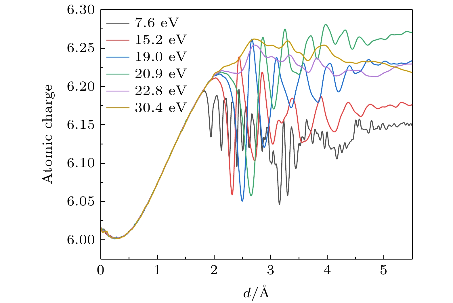
图 6 不同初始动能下, 非绝热模拟中脱离晶格的S原子上的电荷数随d的关系
Figure 6. Number of charges on the sputtered S atom as a function of d with different initial kinetic energies.
-
[1] Bozheyev F, Ellmer K 2022 J. Mater. Chem. A 10 9327
Google Scholar
[2] Khatua D P, Singh A, Gurung S, Khan S, Tanwar M, Kumar R, Jayabalan J 2022 J. Phys. Condens. Matter. 34 155401
Google Scholar
[3] Ganatra R, Zhang Q 2014 ACS Nano 8 4074
Google Scholar
[4] Singh E, Singh P, Kim K S, Yeom G Y, Nalwa H S 2019 ACS Appl. Mater. Interfaces 11 11061
Google Scholar
[5] Nawz T, Safdar A, Hussain M, Sung Lee D, Siyar M 2020 Crystals 10 902
Google Scholar
[6] Sanikop R, Sudakar C 2019 ACS Appl. Nano Mater. 3 576
Google Scholar
[7] Islam M M, Dev D, Krishnaprasad A, Tetard L, Roy T 2020 Sci. Rep. 10 21870
Google Scholar
[8] Wu F, Tian H, Shen Y, Hou Z, Ren J, Gou G Y, Sun Y B, Yang Y, Ren T L 2022 Nature 603 259
Google Scholar
[9] Cao Y 2021 ACS Nano 15 11014
Google Scholar
[10] Zhao G Y, Deng H, Nathaniel T, Michael G, Abdellah L, Peng Q, Yan J A, Wang C D, Lan Y C 2019 Appl. Sci. 9 678
Google Scholar
[11] Pandey M, Rasmussen F A, Kuhar K, Olsen T, Jacobsen K W, Thygesen K S 2016 Nano Lett. 16 2234
Google Scholar
[12] Wang Y Q, Deng L J, Wei Q L, Wan Y, Liu Z, Lu X, Li Y, Bi L, Zhang L, Lu H P, Chen H Y, Zhou P H, Zhang L B, Cheng Y C, Zhao X X, Ye Y, Huang W, Pennycook S J, Loh K P, Peng B 2020 Nano Lett. 20 2129
Google Scholar
[13] Taffelli A, Dirè S, Quaranta A, Pancheri L 2021 Sensors 21 2758
Google Scholar
[14] Sorkin V, Zhou H, Yu Z G, Ang K W, Zhang Y W 2022 Sci. Rep. 12 18001
Google Scholar
[15] Wang Y, Liu S, Li Q, Quhe R, Yang C, Guo Y, Zhang X, Pan Y, Li J, Zhang H, Xu L, Shi B, Tang H, Li Y, Yang J, Zhang Z, Xiao L, Pan F, Lu J 2021 Rep. Prog. Phys. 84 056501
Google Scholar
[16] Cheng Y, Wan R, Li L, Liu Z, Yan S, Li L, Wang J, Gao Y 2022 J. Opt. 24 2040
Google Scholar
[17] Cheng Y, Song H, Wu H, Zhang P, Tang Z, Lu S 2020 Chem. Asian J. 15 3123
Google Scholar
[18] Xie Y, Liang F, Chi S, Wang D, Zhong K, Yu H, Zhang H, Chen Y, Wang J 2020 ACS Appl. Mater. Interfaces 12 7351
Google Scholar
[19] Yang Z, Zhu L, Lü C, Zhang R, Wang H, Wang J, Zhang Q 2021 Mater. Chem. Front. 5 5880
Google Scholar
[20] Komsa H P, Kotakoski J, Kurasch S, Lehtinen O, Kaiser U, Krasheninnikov A V 2012 Phys. Rev. Lett. 109 035503
Google Scholar
[21] Susi T, Meyer J C, Kotakoski J 2019 Nat. Rev. Phys. 1 397
Google Scholar
[22] Yoshimura A, Lamparski M, Kharche N, Meunier V 2018 Nanoscale 10 2388
Google Scholar
[23] Ugurlu O, Haus J, Gunawan A A, Thomas M G, Maheshwari S, Tsapatsis M, Mkhoyan K A 2011 Phys. Rev. B 83 113408
Google Scholar
[24] Lehnert T, Lehtinen O, Algara-Siller G, Kaiser U 2017 Appl. Phys. Lett. 110 033106
Google Scholar
[25] Tai K L, Huang C W, Cai R F, Huang G M, Tseng Y T, Chen J, Wu W W 2020 Small 16 1905516
Google Scholar
[26] Meyer J C, Eder F, Kurasch S, Skakalova V, Kotakoski J, Park H J, Roth S, Chuvilin A, Eyhusen S, Gred B, Krasheninnikov A V, Kaiser U 2012 Phys. Rev. Lett. 108 196102
Google Scholar
[27] Kretschmer S, Lehnert T, Kaiser U, Krasheninnikov A V 2020 Nano Lett. 20 2865
Google Scholar
[28] Runge E, Gross E K 1984 Phys. Rev. Lett. 52 997
Google Scholar
[29] Jia W, Fu J, Cao Z, Wang L, Chi X, Gao W, Wang L W 2013 J. Comput. Phys. 251 102
Google Scholar
[30] Jia W, Cao Z, Wang L, Fu J, Chi X, Gao W, Wang L W 2013 Comput. Phys. Commun. 184 9
Google Scholar
[31] Hamann D R, Schlüter M, Chiang C 1979 Phys. Rev. Lett. 43 1494
Google Scholar
[32] Hamann D R 2013 Phys. Rev. B 88 085117
Google Scholar
[33] Shen Y T, Xu T, Tan X D, He L B, Yin K B, Wan N, Sun L T 2018 Adv. Mater. 30 1705954
Google Scholar
[34] Zener C 1932 Proc. R. Soc. London, Ser. A 137 696
Google Scholar
[35] Olson A J, Wang S J, Niffenegger R J, Li C H, Greene C H, Chen Y P 2014 Phys. Rev. A 90 013616
Google Scholar
[36] Wang L W 2002 Phys. Rev. B 65 153410
Google Scholar

 DownLoad:


Catalog
Metrics
- Abstract views: 2577
- PDF Downloads: 354
- Cited By: 0
