


-
Transition metal dichalcogenides have emerged as a prominent class of two-dimensional layered material, capturing sustained attention from researchers due to their unique structures and properties. These distinctive characteristics render transition metal dichalcogenides highly versatile in numerous fields, including optoelectronics, nanoelectronics, energy storage devices, and electrocatalysis. In particular, the ability to modulate the doping characteristics of these materials plays a crucial role in improving the photoelectric response performance of devices, making it imperative to investigate and understand such effects. In recent years, the electrochemical ion intercalation technique has emerged as a novel approach for precise doping control of two-dimensional materials. Building upon this advancement, this paper aims to demonstrate the effective doping control of transition metal dichalcogenides devices by utilizing the electrochemical ion intercalation method specifically on thick WS2 layers. The results show that the conductivity is significantly improved, which is about 200 times higher than the original value, alongside the achievement of efficient and reversible control over the photoelectric response performance is effectively and reversibly controlled by manipulating the gate voltage. One of the key findings in this work is the successful demonstration of the reversible cyclic control of the photoelectric response in WS2 devices through ion intercalation, regulated by the gate voltage. This dynamic control mechanism showcases the potential for finely tuning and tailoring the performance of photoelectric devices made from two-dimensional materials. The ability to achieve reversible control is especially significant as it allows for a versatile range of applications, enabling devices to be adjusted according to specific requirements and operating conditions. The implications of this work extend beyond the immediate findings and present a foundation for future investigation into response control of photoelectric devices constructed by using two-dimensional materials through the utilization of the ion intercalation method. By establishing the feasibility and efficacy of this technique in achieving controlled doping and precise modulation of photoelectric response, researchers can explore its potential applications in various technological domains. Furthermore, this research serves as a stepping stone for developing the advanced doping strategies, enabling the design and fabrication of high-performance devices with enhanced functionalities. In summary, this work showcases the significance of doping control in transition metal dichalcogenide devices and demonstrates the potential of the electrochemical ion intercalation method for achieving precise modulation of their photoelectric response performance. The observed enhancements in electrical conductivity and the ability to reversibly control the photoelectric response highlight the promising prospects of this technique. Ultimately, this work paves the way for future advancements in the field of two-dimensional materials and opens up new way for designing and optimizing photoelectric devices with improved functionality and performance. -
Keywords:
- WS2 /
- ion intercalation /
- photoelectric response /
- doping control
[1] Khan K, Tareen A K, Aslam M, Wang R H, Zhang Y P, Mahmood A, Ouyang Z B, Zhang H, Guo Z Y 2020 J. Mater. Chem. C 8 387
 Google Scholar
[2] Qiu Q X, Huang Z M 2021 Adv. Mater. 33 2008126
Google Scholar
[3] Yang S X, Chen Y J, Jiang C B 2021 InFoMat. 3 397
Google Scholar
[4] Huang L J, Krasnok A, Alu A, Yu Y L, Neshev D, Miroshnichenko A E 2022 Rep. Prog. Phys. 85 046401
Google Scholar
[5] Amann J, Volkl T, Rockinger T, Kochan D, Watanabe K, Taniguchi T, Fabian J, Weiss D, Eroms J 2022 Phys. Rev. B 105 115425
Google Scholar
[6] Bai Z Q, Xiao Y, Luo Q, Li M M, Peng G, Zhu Z H, Luo F, Zhu M J, Qin S Q, Novoselov K 2022 ACS NANO 16 7880
Google Scholar
[7] Vaquero D, Clerico V, Salvador-Sanchez J, Quereda J, Diez E, Perez-Munoz A M 2021 Micromachines 12 1576
Google Scholar
[8] Qin M S, Han X Y, Ding D D, Niu R R, Qu Z Z, Wang Z Y, Liao Z M, Gan Z Z, Huang Y, Han C R, Lu J M, Ye J T 2021 Nano Lett. 21 6800
Google Scholar
[9] Choi W R, Hong J H, You Y G, Campbell E E B, Jhang S H 2021 Appl. Phys. Lett. 119 223105
Google Scholar
[10] Cao Q, Grote F, Huβmann M, Eigler S 2021 Nanoscale. Adv. 3 963
Google Scholar
[11] Zhou J, Lin Z, Ren H, Duan X, Shakir I, Huang Y, Duan X 2021 Adv. Mater. 33 2004557
Google Scholar
[12] Zhang Z, Wang Y, Zhao Z L, Song W J, Zhou X L, Li Z 2023 Molecules 28 959
Google Scholar
[13] Wu Y C, Li D F, Wu C L, Hwang H Y, Cui Y 2023 Nat. Rev. Mater. 8 41
Google Scholar
[14] Wang Y C, Ou J Z, Balendhran S, et al. 2013 ACS Nano 7 10083
Google Scholar
[15] Yu Y J, Yang F Y, Lu X F, et al. 2015 Nat. Nanotechnol. 10 270
Google Scholar
[16] Xiong F, Wang H T, Liu X G, Sun J, Brongersma M, Pop E, Cui Y 2015 Nano Lett. 15 6777
Google Scholar
[17] Muscher P K, Rehn D A, Sood A, Lim K, Luo D, Shen X, Zajac M, Lu F, Mehta A, Li Y, Wang X, Reed E J, Chueh W C, Lindenberg A M 2021 Adv. Mater. 33 2101875
Google Scholar
[18] Wang M J, Kumar A, Dong H, Woods J M, Pondick J V, Xu S Y, Hynek D J, Guo P J, Qiu D Y, Cha J J 2022 Adv. Mater. 34 2200861
Google Scholar
[19] Novoselov K S, Geim A K, Morozov S V, Jiang D, Zhang Y, Dubonos S V, Grigorieva I V, Firsov A A 2004 Science 306 666
Google Scholar
[20] Bediako D K, Rezaee M, Yoo H, Larson D T, Zhao S Y F, Taniguchi T, Watanabe K, Brower-Thomas T L, Kaxiras E, Kim P 2018 Nature 558 425
Google Scholar
[21] Xiao J, Choi D W, Cosimbescu L, Koech P, Liu J, Lemmon J P 2010 Chem. Mater. 22 4522
Google Scholar
[22] Zhou X S, Wan L J, Guo Y G 2012 Nanoscale 4 5868
Google Scholar
[23] Zhang J S, Yang A K, Wu X, et al. 2018 Nat. Commun. 9 5289
Google Scholar
[24] Wang G, Chernikov A, Glazov M M, Heinz T F, Marie X, Amand T, Urbaszek B 2018 Rev. Mod. Phys. 90 021001
Google Scholar
[25] Li Y L, Chernikov A, Zhang X, Rigosi A, Hill H M, van der Zande A M, Chenet D A, Shih E M, Hone J, Heinz T F 2014 Phys. Rev. B 90 205422
Google Scholar
[26] Zeng H L, Liu G B, Dai J F, Yan Y J, Zhu B R, He R C, Xie L, Xu S J, Chen X H, Yao W, Cui X D 2013 Sci. Rep 3 1608
Google Scholar
[27] Buscema M, Barkelid M, Zwiller V, van der Zant H S J, Steele G A, Castellanos-Gomez A 2013 Nano. Lett. 13 358
Google Scholar
[28] Py M A, Haering R R 1983 Can. J. Phys. 61 76
Google Scholar
[29] Fu D Z, Zhang B W, Pan X C, Fei F C, Chen Y D, Gao M, Wu S Y, He J, Bai Z B, Pan Y M, Zhang Q F, Wang X F, Wu X L, Song F Q 2017 Sci. Rep. 7 12688
Google Scholar
[30] Enyashin A N, Seifert G 2012 Comput. Theor. Chem 999 13
Google Scholar
[31] Liao M H, Wang H, Zhu Y Y, Shang R N, Rafique M, Yang L X, Zhang H, Zhang D, Xue Q K 2021 Nat. Commun. 12 5342
Google Scholar
[32] Zhang X, Qiao X F, Shi W, Wu J B, Jiang D S, Tan P H 2015 Chem. Soc. Rev. 44 2757
Google Scholar
-
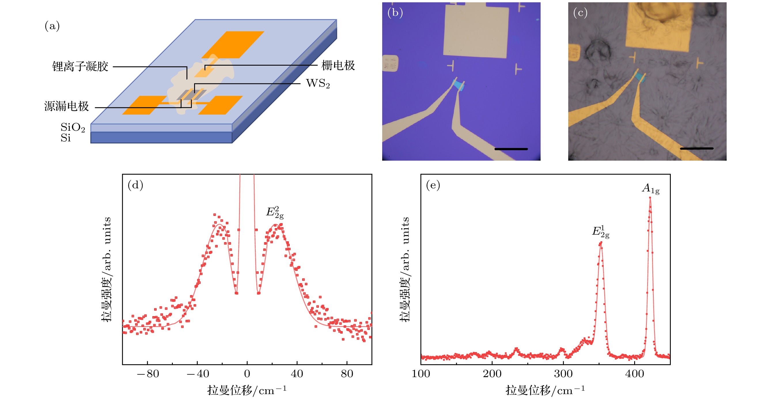
图 1 (a) WS2器件结构示意图; (b)旋涂锂离子凝胶前的WS2器件显微图像, 样品尺寸约为15 μm × 25 μm, 源漏电极宽度约2 μm, 栅电极尺寸约为80 μm×100 μm; (c)旋涂锂离子凝胶后器件显微图像; (d), (e) WS2样品不同波段的拉曼光谱表征, 所有峰位与WS2特征峰吻合. 图中比例尺均为50 μm
Figure 1. (a) Schematic diagram of WS2 device for ion intercalation; (b) optical image of WS2 device before spin coating lithium ion gel, the size of sample is about 15 μm×25 μm, the width of the source and drain electrode is about 2 μm, and the size of the gate electrode is about 80 μm×100 μm; (c) optical image of device after spin coating lithium ion gel; (d), (e) Raman spectra characterization of the bulk WS2, all the peaks showed in Raman spectra are consistent with the characteristic peaks of WS2. The scale bars are 50 μm.
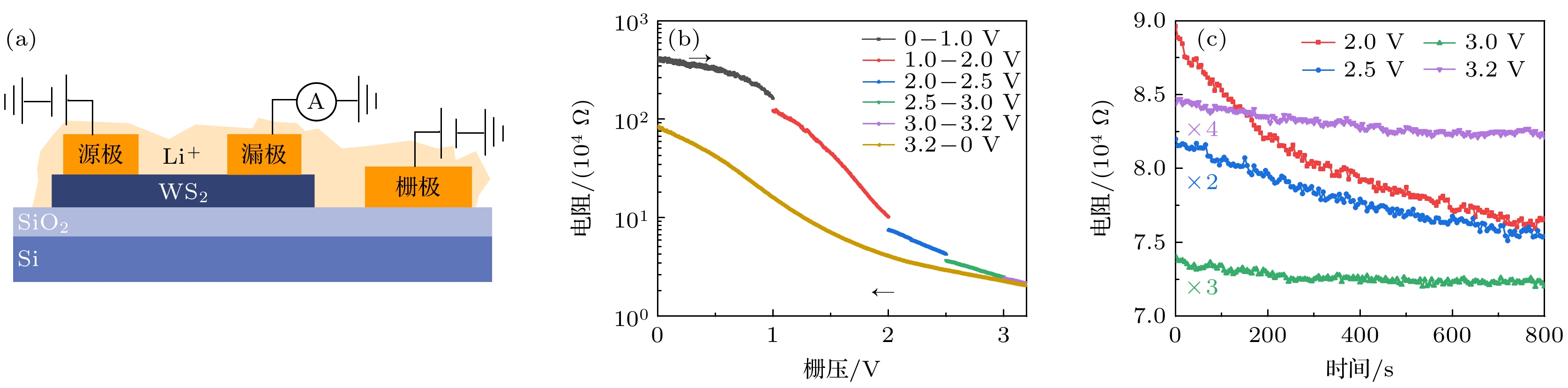
图 2 WS2器件源漏间电阻的栅压依赖测试 (a)离子插层过程电阻的测试示意图, 在栅电极施加不同栅压VG, 源电极施加偏压VB = 0.5 V, 漏电极读取不同VG下的电流值; (b) WS2电阻随栅压VG变化的曲线, 栅压变化的速率为1 mV/s. 图中箭头表示增加栅压(插层, Li+ 进入WS2)和减小栅压(去插层, Li+离开WS2)的过程; (c) WS2电阻随时间的变化曲线, 其中不同颜色的曲线代表测试时在不同的栅压停留
Figure 2. Gate voltage dependence of source-drain resistance of WS2 devices: (a) Schematic diagram of resistance measurement during ion intercalation, gate voltage VG was applied from the gate electrode with a bias voltage of VB = 0.5 V at the source electrode, the currents under different VG were measured at the drain electrode; (b) gate voltage dependence of WS2 device resistance, gate voltage changes at a rate of 1 mV/s, the arrows in the figure represent the process of increasing gate voltage (intercalation, Li+ moving towards WS2) and decreasing gate voltage (de-intercalation, Li+ leaving WS2); (c) time dependence of WS2 resistance at given gate voltages during intercalation, waiting at different gate voltages is represented by curves in different colors.

图 3 零偏压下WS2器件的扫描光电流图像随栅压的变化, 激发光波长为633 nm, 功率为80 μW, 使用40×物镜进行聚焦, 聚焦后光斑直径约4 μm (a)零栅压下的扫描反射图像; (b)—(h) 不同栅压下的扫描光电流图像, 标注数值为栅压大小, 黑色箭头表示插层(增大栅压, Li+进入WS2)和去插层(减小栅压, Li+离开WS2)的过程. 图中所有比例尺为10 μm
Figure 3. Scanning photocurrent images of WS2 device under 633 nm excitation light with a power of 80 μW at 0 V bias, the excitation light is focused using a 40× objective lens and the focused spot size is about 4 μm: (a) Scanning reflection image under 0 V gate voltage; (b)–(h) scanning photocurrent images at different gate voltages, the marked value is the magnitude of gate voltage, and the black arrows represent the intercalation (increasing gate voltage, Li+ moving towards WS2) and de-intercalation (decreasing gate voltage, Li+ leaving WS2) processes. The scale bars are 10 μm.
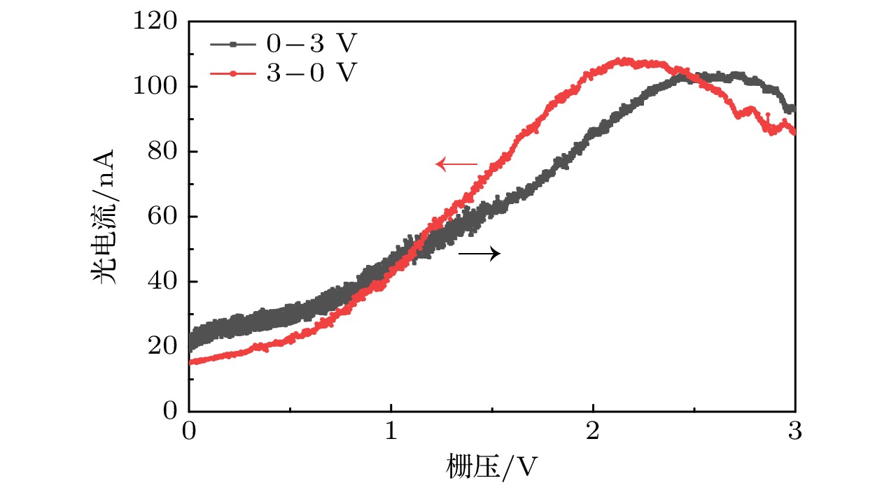
图 4 零偏压下WS2器件的光电流响应的栅压依赖曲线. 激发光波长为633 nm、功率为80 μW, 激光光斑位置为图3(e)中白色圆圈, 栅压变化的速率为0.1 mV/s, 黑色箭头和曲线代表增大栅压(插层)的过程, 红色箭头和曲线表示减小栅压(去插层)的过程
Figure 4. Gate voltage dependence of photocurrent of WS2 device at 0 V bias, the wavelength of excitation light is 633 nm and the power is 80 μW, the white circle in Fig. 3(e) indicates the focus position of laser, gate voltage changes at a rate of 0.1 mV/s, the black arrow and curve show the process of increasing gate voltage (intercalation), and the red arrow and curve show the process of decreasing gate voltage (de-intercalation).

图 5 零偏压下WS2器件的扫描光电流图像随栅压的变化 (a)—(h)激发光波长为880 nm、功率为80 μW, 其中(a)是零栅压下WS2器件的扫描反射图像; (b)—(h) WS2器件在不同栅压下的扫描光电流图像; (i)—(p)激发光波长为1000 nm, 功率为80 μW, 其中(i)是零栅压下WS2的扫描反射图像, (g)—(p) WS2器件在不同栅压下的扫描光电流图像. 所有比例尺都为5 μm
Figure 5. Scanning photocurrent images of WS2 device under different gate voltages at 0 V bias voltage: (a)–(h) Excitation light wavelength is 880 nm, power is 80 μW, (a) the scanning reflection image of the WS2 device at 0 V gate voltage; (b)–(h) the scanning photocurrent images of the WS2 device at different gate voltages; (i)–(p) excitation light wavelength is 1000 nm, power is 80 μW, (i) the scanning reflection image of WS2 at 0 V gate voltage; (g)–(p) the scanning photocurrent images of the WS2 device at different gate voltages. The scale bars are 5 μm.
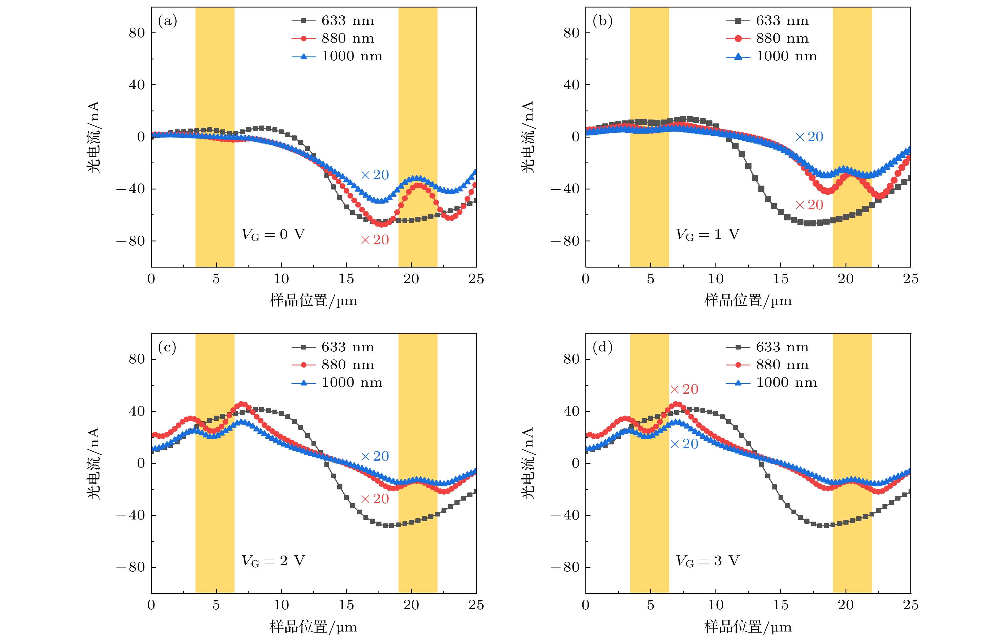
图 6 WS2器件中央切线处的光电流响应在离子插层过程对于激发光的波长依赖曲线 (a)—(d)在不同栅压的条件下, VG = 0 V, VG = 1 V, VG = 2 V, VG = 3 V, 激发光功率为80 μW, 波长分别为633 nm (黑色)、880 nm (红色)、1000 nm (蓝色), 切线位置分别为图3(b)和图5(b), (j)中红色箭头对应的样品位置, 黄色填充部分表示电极区域
Figure 6. Wavelength dependence of photocurrent at the center line of WS2 device in the ion intercalation process: (a) VG = 0 V, (b) VG = 1 V, (c), VG = 2 V, (d) VG = 3 V are the conditions of different gate voltages. The excitation light power is 80 μW, and the wavelengths are 633 nm (black), 880 nm (red), and 1000 nm (blue), respectively. The sample positions corresponding to the red arrows in Figs. 3(b), 5(b), (j) represent the linecut positions. The yellow filled parts are the electrode area.

图 7 WS2器件的归一化光电流谱, 激光光斑位置为图10(c)中红色圆圈, 激发光波长范围为500—1020 nm, 测试波长间隔为10 nm, 520 nm与620 nm波长处的两个响应峰值对应于WS2的两个激子吸收峰, 插图为激光波长范围为700—1020 nm的归一化光电流谱
Figure 7. Normalized photocurrent spectrum of WS2 device. The red circle in Fig. 10(c) indicates the focus position of laser, the laser wavelength range of the measurement is 500—1020 nm, and the wavelength step is 10 nm. The two peaks at 520 nm and 620 nm correspond to the absorption peaks of two excitons of WS2. The inset shows the normalized photocurrent spectrum of the range 700–1020 nm.

图 8 (a)—(c) WS2器件中央切线处在离子插层过程(增大栅压)的光电流响应; (d)—(f)离子插层前在VG = 0 V和去插层后在VG = 0 V时中央切线处的光电流响应对比, 激发光功率为80 μW, 波长分别为633 nm (a), (d), 880 nm (b), (e), 1000 nm (c), (f). 横坐标表示图3(b), 5(b), (j)中红色箭头对应的样品位置, 纵坐标为对应位置的光电流大小
Figure 8. (a)–(c) Photocurrent at the center line of WS2 device during ion intercalation (increasing gate voltage); (d)–(f) comparison of linecut photocurrent at VG = 0 V before intercalation and after intercalation, excitation light power is 80 μW, wavelengths are (a), (d) 633 nm, (b), (e) 880 nm, (c), (f) 1000 nm, respectively. The x-coordinate represents the sample position corresponding to the red arrows in Fig. 3(b), 5(b), (j), and the y-coordinate represents the photocurrent at the corresponding position.
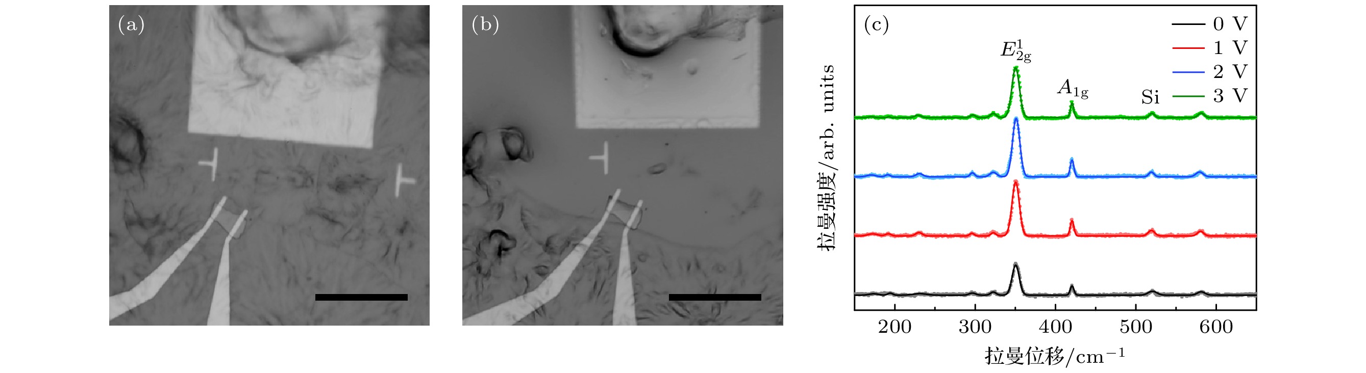
图 9 WS2样品在插层过程中的显微图像和拉曼光谱 (a) VG = 0 V时, 未离子插层前的器件显微图像; (b) VG = 3 V时, 离子插入后的器件显微图像. 图中比例尺均为50 μm; (c)不同栅压下的拉曼光谱, 激发光波长为532 nm, 功率为1 mW, 激光光斑位置为图3(e)中白色圆圈位置, 取样积分时间为5 s. 在增大栅压进行离子插层时, 分别在VG = 0 V (黑色), VG = 1 V (红色), VG = 2 V (蓝色), VG = 3 V (绿色)处采取WS2拉曼信号. 图中标注出的峰位与2H-WS2特征峰一致
Figure 9. Optical images and Raman spectra of WS2 device during intercalation: (a) VG = 0 V, the optical image before ion intercalation; (b) VG = 3 V, the optical image after ion intercalation. The scale bars are 50 μm; (c) Raman spectra of WS2 at different gate, the excitation light wavelength is 532 nm, the power is 1 mW. The white circle in Fig. 3(e) is the focus position of laser and the sampling integration time is 5 s. When increasing gate voltage for ion intercalation, WS2 Raman signals are taken at VG = 0 V (black), VG = 1 V (red), VG = 2 V (blue), VG = 3 V (green). The peak marked in the figure is consistent with the characteristic peak of 2H-WS2.
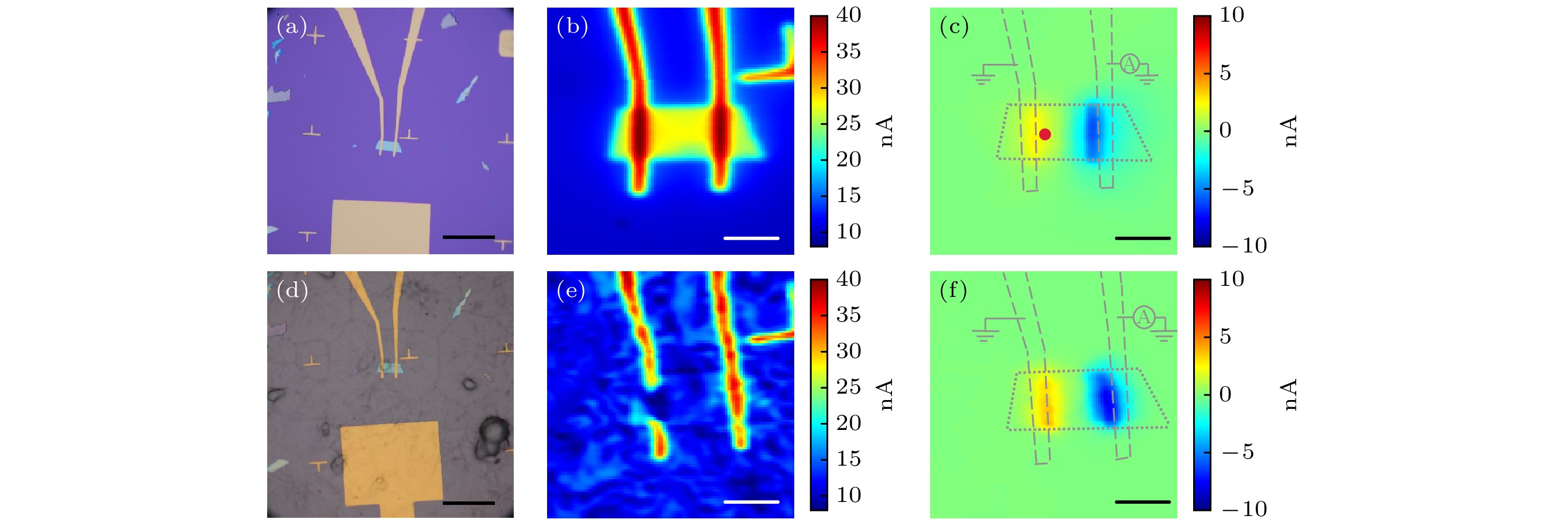
图 10 WS2器件在旋涂锂离子凝胶前后的扫描光电流图像对比 (a), (d)旋涂锂离子凝胶前后的器件图像, 比例尺为50 μm. 零偏压下, 旋涂锂离子凝胶前后的扫描反射图像(b), (e)和扫描光电流响应图像(c), (f). 激发光波长为633 nm, 功率为80 μm, 比例尺为10 μm
Figure 10. Scanning photocurrent images of WS2 device before and after spinning coating lithium ion gel. (a), (d) Optical images of WS2 device before and after spin coating lithium ion gel, the scale bars are 50 μm. Scanning reflection images (b), (e) and scanning photocurrent images (c), (f) of corresponding position before and after spin coating lithium ion gel at 0 V bias. Excitation wavelength is 633 nm, power is 80 μm, the scale bars are 10 μm.
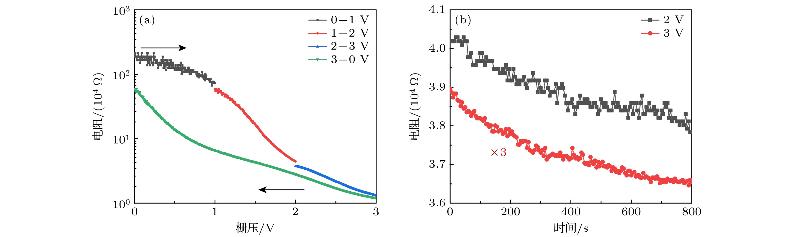
图 11 WS2器件源漏间电阻的栅压依赖测试 (a) WS2电阻随栅压VG变化的曲线, 栅压变化的速率为1 mV/s, 图中箭头同样表示增加栅压(插层, Li+进入WS2)和减小栅压(去插层, Li+离开WS2)的过程; (b) WS2电阻随时间的变化曲线
Figure 11. Gate voltage dependence of source-drain resistance the WS2 device: (a) Gate dependence of WS2 device resistance, gate voltage changes at a rate of 1 mV/s, the arrows in the figure represent the process of increasing gate voltage (intercalation, Li+ moving towards WS2) and decreasing gate voltage (de-intercalation, Li+ leaving WS2); (b) time dependence of WS2 resistance at given gate voltages during intercalation.
-
[1] Khan K, Tareen A K, Aslam M, Wang R H, Zhang Y P, Mahmood A, Ouyang Z B, Zhang H, Guo Z Y 2020 J. Mater. Chem. C 8 387
Google Scholar
[2] Qiu Q X, Huang Z M 2021 Adv. Mater. 33 2008126
Google Scholar
[3] Yang S X, Chen Y J, Jiang C B 2021 InFoMat. 3 397
Google Scholar
[4] Huang L J, Krasnok A, Alu A, Yu Y L, Neshev D, Miroshnichenko A E 2022 Rep. Prog. Phys. 85 046401
Google Scholar
[5] Amann J, Volkl T, Rockinger T, Kochan D, Watanabe K, Taniguchi T, Fabian J, Weiss D, Eroms J 2022 Phys. Rev. B 105 115425
Google Scholar
[6] Bai Z Q, Xiao Y, Luo Q, Li M M, Peng G, Zhu Z H, Luo F, Zhu M J, Qin S Q, Novoselov K 2022 ACS NANO 16 7880
Google Scholar
[7] Vaquero D, Clerico V, Salvador-Sanchez J, Quereda J, Diez E, Perez-Munoz A M 2021 Micromachines 12 1576
Google Scholar
[8] Qin M S, Han X Y, Ding D D, Niu R R, Qu Z Z, Wang Z Y, Liao Z M, Gan Z Z, Huang Y, Han C R, Lu J M, Ye J T 2021 Nano Lett. 21 6800
Google Scholar
[9] Choi W R, Hong J H, You Y G, Campbell E E B, Jhang S H 2021 Appl. Phys. Lett. 119 223105
Google Scholar
[10] Cao Q, Grote F, Huβmann M, Eigler S 2021 Nanoscale. Adv. 3 963
Google Scholar
[11] Zhou J, Lin Z, Ren H, Duan X, Shakir I, Huang Y, Duan X 2021 Adv. Mater. 33 2004557
Google Scholar
[12] Zhang Z, Wang Y, Zhao Z L, Song W J, Zhou X L, Li Z 2023 Molecules 28 959
Google Scholar
[13] Wu Y C, Li D F, Wu C L, Hwang H Y, Cui Y 2023 Nat. Rev. Mater. 8 41
Google Scholar
[14] Wang Y C, Ou J Z, Balendhran S, et al. 2013 ACS Nano 7 10083
Google Scholar
[15] Yu Y J, Yang F Y, Lu X F, et al. 2015 Nat. Nanotechnol. 10 270
Google Scholar
[16] Xiong F, Wang H T, Liu X G, Sun J, Brongersma M, Pop E, Cui Y 2015 Nano Lett. 15 6777
Google Scholar
[17] Muscher P K, Rehn D A, Sood A, Lim K, Luo D, Shen X, Zajac M, Lu F, Mehta A, Li Y, Wang X, Reed E J, Chueh W C, Lindenberg A M 2021 Adv. Mater. 33 2101875
Google Scholar
[18] Wang M J, Kumar A, Dong H, Woods J M, Pondick J V, Xu S Y, Hynek D J, Guo P J, Qiu D Y, Cha J J 2022 Adv. Mater. 34 2200861
Google Scholar
[19] Novoselov K S, Geim A K, Morozov S V, Jiang D, Zhang Y, Dubonos S V, Grigorieva I V, Firsov A A 2004 Science 306 666
Google Scholar
[20] Bediako D K, Rezaee M, Yoo H, Larson D T, Zhao S Y F, Taniguchi T, Watanabe K, Brower-Thomas T L, Kaxiras E, Kim P 2018 Nature 558 425
Google Scholar
[21] Xiao J, Choi D W, Cosimbescu L, Koech P, Liu J, Lemmon J P 2010 Chem. Mater. 22 4522
Google Scholar
[22] Zhou X S, Wan L J, Guo Y G 2012 Nanoscale 4 5868
Google Scholar
[23] Zhang J S, Yang A K, Wu X, et al. 2018 Nat. Commun. 9 5289
Google Scholar
[24] Wang G, Chernikov A, Glazov M M, Heinz T F, Marie X, Amand T, Urbaszek B 2018 Rev. Mod. Phys. 90 021001
Google Scholar
[25] Li Y L, Chernikov A, Zhang X, Rigosi A, Hill H M, van der Zande A M, Chenet D A, Shih E M, Hone J, Heinz T F 2014 Phys. Rev. B 90 205422
Google Scholar
[26] Zeng H L, Liu G B, Dai J F, Yan Y J, Zhu B R, He R C, Xie L, Xu S J, Chen X H, Yao W, Cui X D 2013 Sci. Rep 3 1608
Google Scholar
[27] Buscema M, Barkelid M, Zwiller V, van der Zant H S J, Steele G A, Castellanos-Gomez A 2013 Nano. Lett. 13 358
Google Scholar
[28] Py M A, Haering R R 1983 Can. J. Phys. 61 76
Google Scholar
[29] Fu D Z, Zhang B W, Pan X C, Fei F C, Chen Y D, Gao M, Wu S Y, He J, Bai Z B, Pan Y M, Zhang Q F, Wang X F, Wu X L, Song F Q 2017 Sci. Rep. 7 12688
Google Scholar
[30] Enyashin A N, Seifert G 2012 Comput. Theor. Chem 999 13
Google Scholar
[31] Liao M H, Wang H, Zhu Y Y, Shang R N, Rafique M, Yang L X, Zhang H, Zhang D, Xue Q K 2021 Nat. Commun. 12 5342
Google Scholar
[32] Zhang X, Qiao X F, Shi W, Wu J B, Jiang D S, Tan P H 2015 Chem. Soc. Rev. 44 2757
Google Scholar

 DownLoad:
Catalog
Metrics
- Abstract views: 1710
- PDF Downloads: 156
- Cited By: 0
