


-
Transition metal dichalcogenide (TMDC) monolayers exhibit enhanced electrical and optoelectrical properties, which are promising for next-generation optoelectronic devices. However, large-scale and uniform growth of TMDC monolayers with large grain size is still a considerable challenge. Presented in this work is a simple and effective approach to fabricating largescale molybdenum (MoS2) disulfide monolayers by chemical vapor deposition (CVD) method. It is found that MoS2 grows from single crystal into thin film with the increase of oxide precursor proportion. The photodetector of large scale monolayer layer MoS2 film is fabricated by depositing metal electrodes on the interdigital electrode mask through using thermal evaporation coating. Finally, the highly stable and repeatable photoelectric responses under the conditions of different voltages and different laser power are characterized under 405-nm laser excitation, with response time decreasing down to the order of milliseconds (ms). In addition, the photodetector achieves a wide spectral detection range from 405 nm to 830 nm, that is, from visible light to near-infrared light wavelength range, with optical response (R) of 291.7 mA/W and optical detection rate (D*) of 1.629×10⁹ Jones. The monolayer MoS2 thin film photodetector demonstrated here has the advantages of low cost, feasibility of large-scale preparation, and good stability and repeatability in the wide spectrum range from visible light to near infrared light wavelength, providing the possibilities for future applications of electronic and optoelectronic devices .
-
Keywords:
- MoS2 /
- chemical vapor deposition /
- photodetector /
- photoelectric response
[1] Gao G Y, Yu J, Yang X X, Pang Y K, Zhao J, Pan C F, Sun Q J, Wang Z L 2018 Adv. Mater. 31 1806905
[2] Li X F, Yang L M, Si M W, Li S C, Huang M Q, Ye P D, Wu Y Q 2015 Adv. Mater. 27 1547
 Google Scholar
[3] Radisavljevic B, Radenovic A, Brivio J, Giacometti V, Kis A 2011 Nat. Nanotechnol. 6 147
Google Scholar
[4] Kaushik V, Ahmad M, Agarwal K, Varandani D, Belle B D, Das P, Mehta B R 2020 J. Phys. Chem. C 124 23368
Google Scholar
[5] Bagot P A J, Silk O B W, Douglas J O, Pedrazzini S, Crudden D J, Martin T L, Hardy M C, Moody M P, Reed R C 2017 Acta Mater. 125 156
Google Scholar
[6] Wang X D, Wang P, Wang J L, Hu W D, Zhou X H, Guo N, Huang H, Sun S, Shen H, Lin T, Tang M H, Liao L, Jiang A Q, Sun J L, Meng X J, Chen X S, Lu W, Chu J H 2015 Adv. Mater. 27 6575
Google Scholar
[7] Huang Z Z, Zhang T F, Liu J K, Zhang L H, Jin Y H, Wang J P, Jiang K, Fan S, Li Q Q 2019 ACS Appl. Electron. Mater. 1 1314
Google Scholar
[8] Furchi M M, Polyushkin D K, Pospischil A, Mueller T 2014 Nano Lett. 14 6165
Google Scholar
[9] Lee J, Pak S, Lee Y W, Cho Y, Hong J, Giraud P, Shin H S, Morris S M, Sohn J I, Cha S, Kim J M 2017 Nat. Commun. 8 14734
Google Scholar
[10] Lee D, Hwang E, Lee Y, Choi Y, Kim J S, Lee S, Cho J H 2016 Adv. Mater. 28 9196
Google Scholar
[11] Choi M S, Lee G H, Yu Y J, Lee D Y, Lee S H, Kim P, Hone J, Yoo W J 2013 Nat. Commun. 4 1624
Google Scholar
[12] Chen Y F, Wang Y, Wang Z, Gu Y, Ye Y, Chai X L, Ye J F, Chen Y, Xie R Z, Zhou Y, Hu Z G, Li Q, Zhang L L, Wang F, Wang P, Miao J S, Wang J L, Chen X S, Lu W, Zhou P, Hu W D 2021 Nat. Electron. 4 357
Google Scholar
[13] Wu P S, Ye L, Tong L, Wang P, Wang Y, Wang H L, Ge H N, Wang Z, Gu Y, Zhang K, Yu Y Y, Peng M, Wang F, Huang M, Zhou P, Hu W D 2022 Light Sci. Appl. 11 6
Google Scholar
[14] Van Der Zande A M, Huang P Y, Chenet D A, Berkelbach T C, You Y, Lee G H, Heinz T F, Reichman D R, Muller D A, Hone J C 2013 Nat. Mater. 12 554
Google Scholar
[15] Lee H S, Min S W, Chang Y G, Park M K, Nam T, Kim H, Kim J H, Ryu S, Im S 2012 Nano Lett. 12 3695
Google Scholar
[16] Mak K F, Lee C, Hone J, Shan J, Heinz T F 2010 Phys. Rev. Lett. 105 136805
Google Scholar
[17] Li H, Wu J B, Ran F R, Lin M L, Liu X L, Zhao Y Y, Lu X, Xiong Q H, Zhang J, Huang W, Zhang H, Tan P H 2017 ACS Nano 11 11714
Google Scholar
[18] Novoselov K S, Geim A K, Morozov S V, Jiang D, Zhang Y, Dubonos S V, Grigorieva I V, Firsov A A 2004 Science 306 666
Google Scholar
[19] Wang L, Meric I, Huang P Y, Gao Q, Gao Y, Tran H, Taniguchi T, Watanabe K, Campos L M, Muller D A, Guo J, Kim P, Hone J, Shepard K L, Dean C R 2013 Science 342 614
Google Scholar
[20] Yi M, Shen Z G 2015 J. Mater. Chem. A 3 11700
Google Scholar
[21] Ren S, Rong P, Yu Q 2018 Ceramics Int. 44 11940
Google Scholar
[22] Withers F, Yang H, Britnell L, Rooney A P, Lewis E, Felten A, Woods C R, Sanchez Romaguera V, Georgiou T, Eckmann A, Kim Y J, Yeates S G, Haigh S J, Geim A K, Novoselov K S, Casiraghi C 2014 Nano Lett. 14 3987
Google Scholar
[23] Dean C R, Young A F, Meric I, Lee C, Wang L, Sorgenfrei S, Watanabe K, Taniguchi T, Kim P, Shepard K L, Hone J 2010 Nat. Nanotechnol. 5 722
Google Scholar
[24] Sharma M, Singh A, Aggarwal P, Singh R 2022 ACS Omega 7 11731
Google Scholar
[25] Fu D, Zhao X, Zhang Y Y, Li L, Xu H, Jang A R, Yoon S I, Song P, Poh S M, Ren T 2017 J. Am. Chem. Soc. 139 9392
Google Scholar
[26] Lee C H, Zhang Y, Johnson J M, Koltun R, Gambin V, Jamison J S, Myers R C, Hwang J, Rajan S 2020 Appl. Phys. Lett. 117 123102
Google Scholar
[27] Jie W J, Yang Z B, Zhang F, Bai G X, Leung C W, Hao J H 2017 ACS Nano 11 6950
Google Scholar
[28] Kodu M, Avarmaa T, Jaaniso R, Leemets K, Mändar H, Nagirnyi V 2016 Superlattices Microstruct. 98 18
Google Scholar
[29] Wang J, Fan L, Wang X M, Xiao T T, Peng L P, Wang X M, Yu J, Cao L H, Xiong Z W, Fu Y J, Wang C B, Shen Q, Wu W D 2019 Appl. Surf. Sci. 494 651
Google Scholar
[30] Gong Y J, Lin J H, Wang X L, Shi G, Lei S D, Lin Z, Zou X L, Ye G L, Vajtai R, Yakobson B I, Terrones H, Terrones M, Tay B K, Lou J, Pantelides S T, Liu Z, Zhou W, Ajayan P M 2014 Nat. Mater. 13 1135
Google Scholar
[31] Hu S, Wang X F, Meng L, Yan X 2017 J. Mater. Sci. 52 7215
Google Scholar
[32] Liu P Y, Luo T, Xing J, Xu H, Hao H Y, Liu H, Dong J J 2017 Nanoscale Res. Lett. 12 558
Google Scholar
[33] Li M G, Yao J D, Wu X X, Zhang S C, Xing B R, Niu X Y, Yan X Y, Yu Y, Liu Y L, Wang Y W 2020 ACS Appl. Mater. Interfaces 12 6276
Google Scholar
[34] Li J, Yang X D, Liu Y, Huang B L, Wu R X, Zhang Z W, Zhao B, Ma H F, Dang W Q, Wei Z, Wang K, Lin Z Y, Yan X X, Sun M Z, Li B, Pan X Q, Luo J, Zhang G Y, Liu Y, Huang Y, Duan X D, Duan X F 2020 Nature 579 368
Google Scholar
[35] Zhang Z W, Huang Z W, Li J, Wang D, Lin Y, Yang X D, Liu H, Liu S, Wang Y L, Li B, Duan X F, Duan X D 2022 Nat. Nanotechnol. 17 493
Google Scholar
[36] Lopez-Sanchez O, Lembke D, Kayci M, Radenovic A, Kis A 2013 Nat. Nanotechnol. 8 497
Google Scholar
[37] Zhang W, Huang J K, Chen C H, Chang Y H, Cheng Y J, Li L J 2013 Adv. Mater. 25 3456
Google Scholar
[38] Di Bartolomeo A, Genovese L, Foller T, Giubileo F, Luongo G, Croin L, Liang S J, Ang L K, Schleberger M 2017 Nanotechnology 28 214002
Google Scholar
[39] Nie C B, Yu L Y, Wei X Z, Shen J, Lu W Q, Chen W M, Feng S L, Shi H F 2017 Nanotechnology 28 275203
Google Scholar
[40] Han P, St Marie L, Wang Q X, Quirk N, El Fatimy A, Ishigami M, Barbara P 2018 Nanotechnology 29 20LT01
Google Scholar
[41] Pak Y, Park W, Mitra S, Sasikala Devi A A, Loganathan K, Kumaresan Y, Kim Y, Cho B, Jung G Y, Hussain M M, Roqan I S 2018 Small 14 201703176
[42] Radisavljevic B, Kis A 2013 Nat. Mater. 12 815
Google Scholar
[43] Wang J, Yao Q, Huang C W, Zou X, Liao L, Chen S, Fan Z, Zhang K, Wu W, Xiao X, Jiang C, Wu W W 2016 Adv. Mater. 28 8302
Google Scholar
[44] Li Y N, Li L N, Li S S, Sun J Y, Fang Y, Deng T 2022 ACS Omega 7 13615
Google Scholar
[45] Zhao T G, Guo J X, Li T T, Wang Z, Peng M, Zhong F, Chen Y, Yu Y Y, Xu T F, Xie R Z, Gao P Q, Wang X R, Hu W D 2023 Chem. Soc. Rev. 52 1650
Google Scholar
[46] Suleman M, Lee S, Kim M, Nguyen V H, Riaz M, Nasir N, Kumar S, Park H M, Jung J, Seo Y 2022 ACS Omega 7 30074
Google Scholar
[47] Sun P, Liu Y W, Ma J, Li W, Zhang K L, Yuan Y J 2019 CrystEngComm 21 6969
Google Scholar
[48] Zhao T G, Zhong F, Wang S C, Wang Y K, Xu T F, Chen Y, Yu Y Y, Guo J X, Wang Z, Yu J C, Gao P Q 2022 Adv. Opt. Mater. 11 2202208
[49] Sinha S, Kumar S, Arora SK, Sharma A, Tomar M, Wu H C, Gupta V 2021 J. Appl. Phys. 129 155304
Google Scholar
-
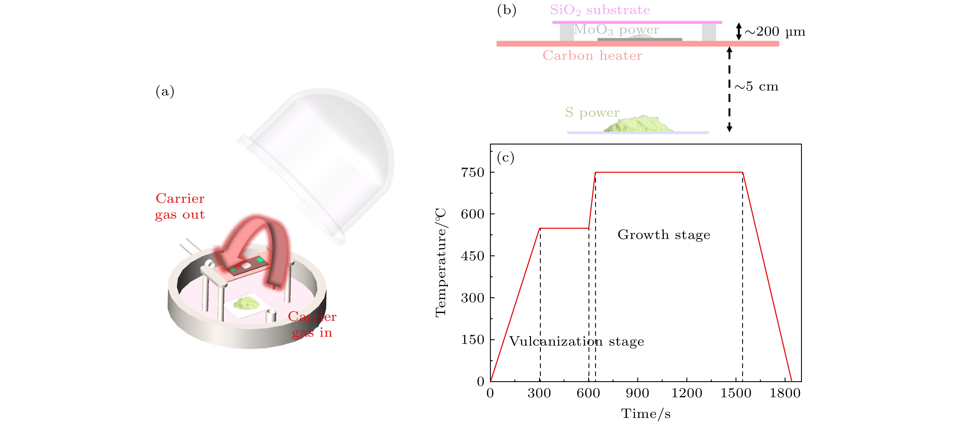
图 1 (a) CVD生长单层MoS2薄膜实验装置示意图; (b)化学反应区放大图; (c) CVD生长过程温度曲线
Figure 1. (a) CVD experimental equipment for MoS2 synthesis; (b) enlarged view of the chemical reaction zone; (c) temperature curve of CVD growth process.
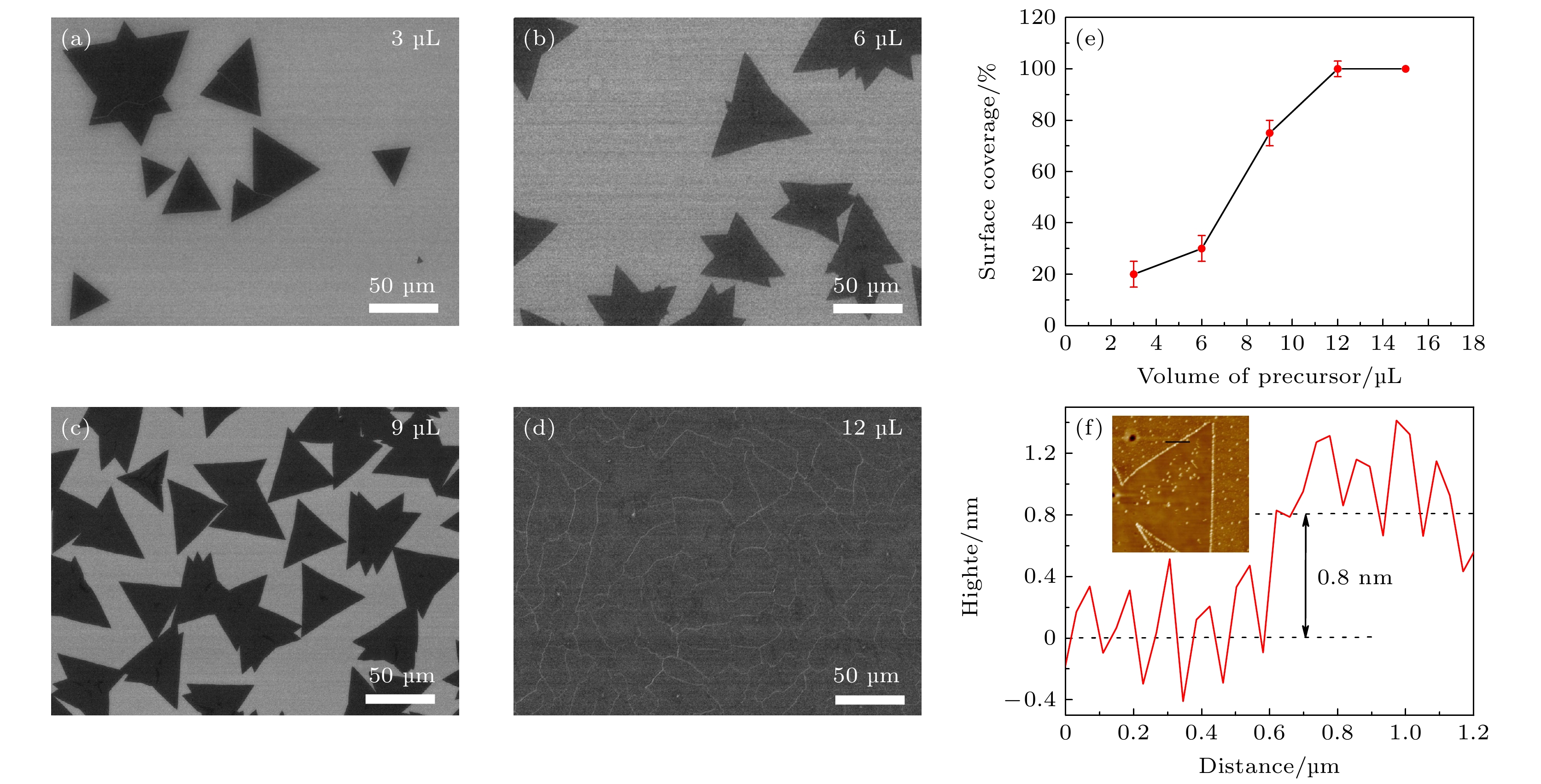
图 2 (a)—(d)不同MoO3前驱体量下制备的MoS2的SEM形貌; (e) MoS2覆盖率随前驱体量的变化曲线; (f) MoS2的AFM照片(插图)和图中黑线高度随位置的变化曲线
Figure 2. (a)–(d) SEM morphologies of MoS2 prepared under different volumes of MoO3 precursor; (e) curve of MoS2 coverage with precursor volume; (f) the height of MoS2 as a function of position marked as black line in the inset, inset is AFM photograph of MoS2.
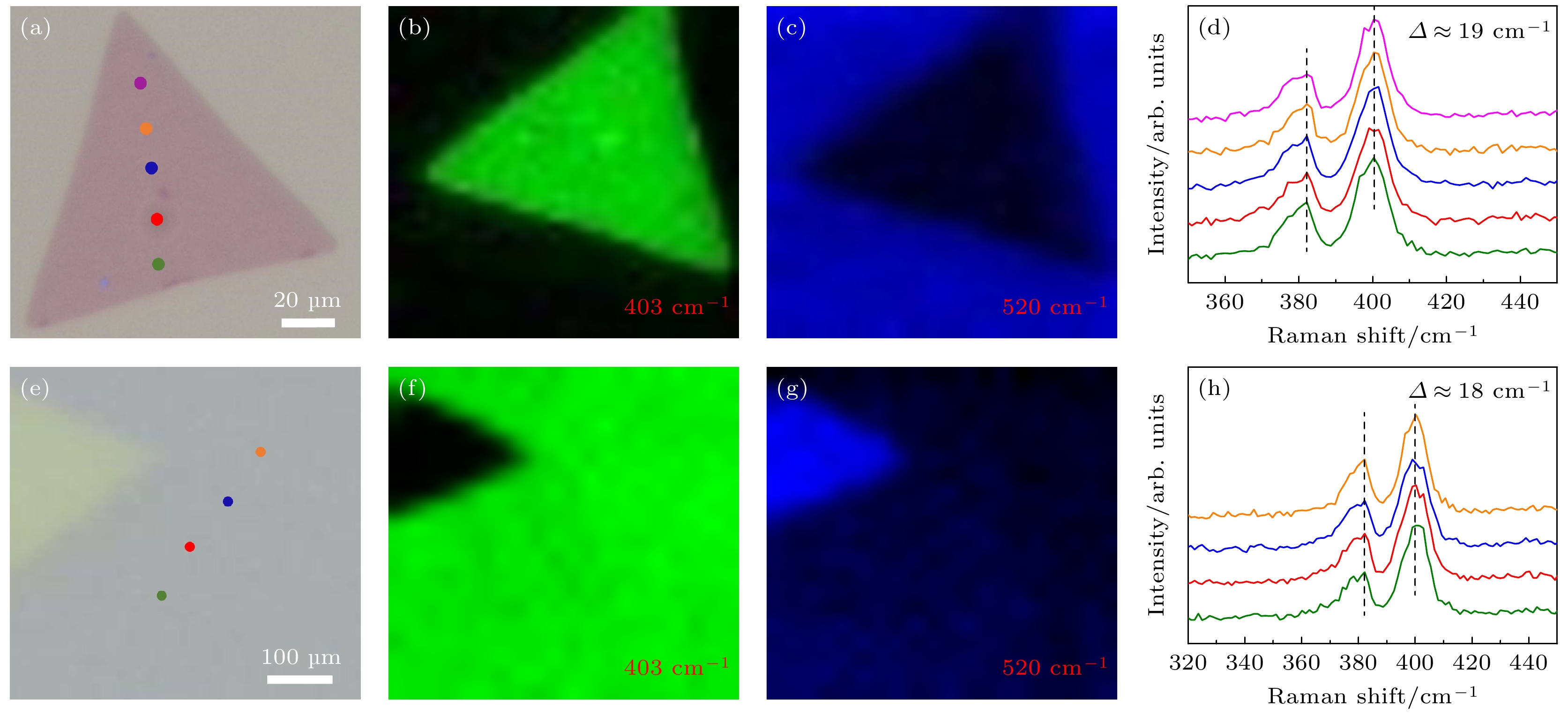
图 3 (a) MoS2单晶光学显微镜图像; (b)单晶MoS2的拉曼成像; (c) Si/SiO2基底拉曼成像; (d)对应图(a)中各点的拉曼光谱; (e) MoS2薄膜的光学显微镜图像; (f) MoS2薄膜的拉曼成像; (g) Si/SiO2基底拉曼成像; (h)图(e)各点对应的拉曼光谱
Figure 3. (a) Optical microscope image of single crystal MoS2; (b) Raman mapping of single crystal MoS2; (c) Raman mapping of Si/SiO2 substrate; (d) Raman spectra of each point in Fig. (a); (e) optical microscope image of thin film MoS2; (f) Raman mapping of thin film MoS2; (g) Raman mapping of Si/SiO2 substrate; (h) Raman spectra of each point in Fig. (e).
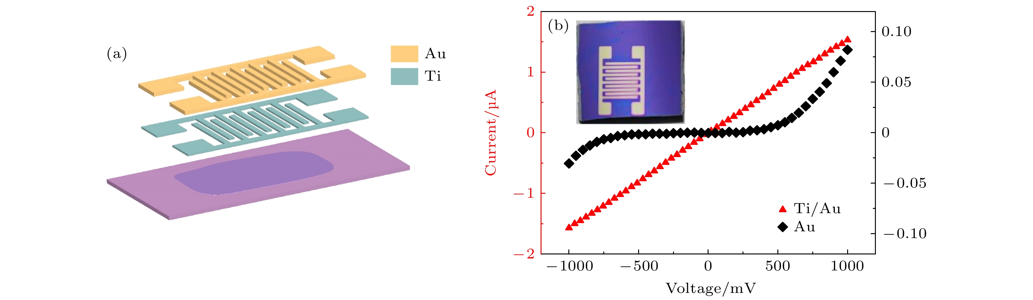
图 4 (a)叉指电极装置示意图; (b) Au和Ti/Au电极上的电流和电压曲线, 插图是MoS2叉指器件实物图
Figure 4. (a) Schematic diagram of interdigital device; (b) the current and voltage curve with Au and Ti/Au electrodes, the inset shows the image of the MoS2 interdigital device.
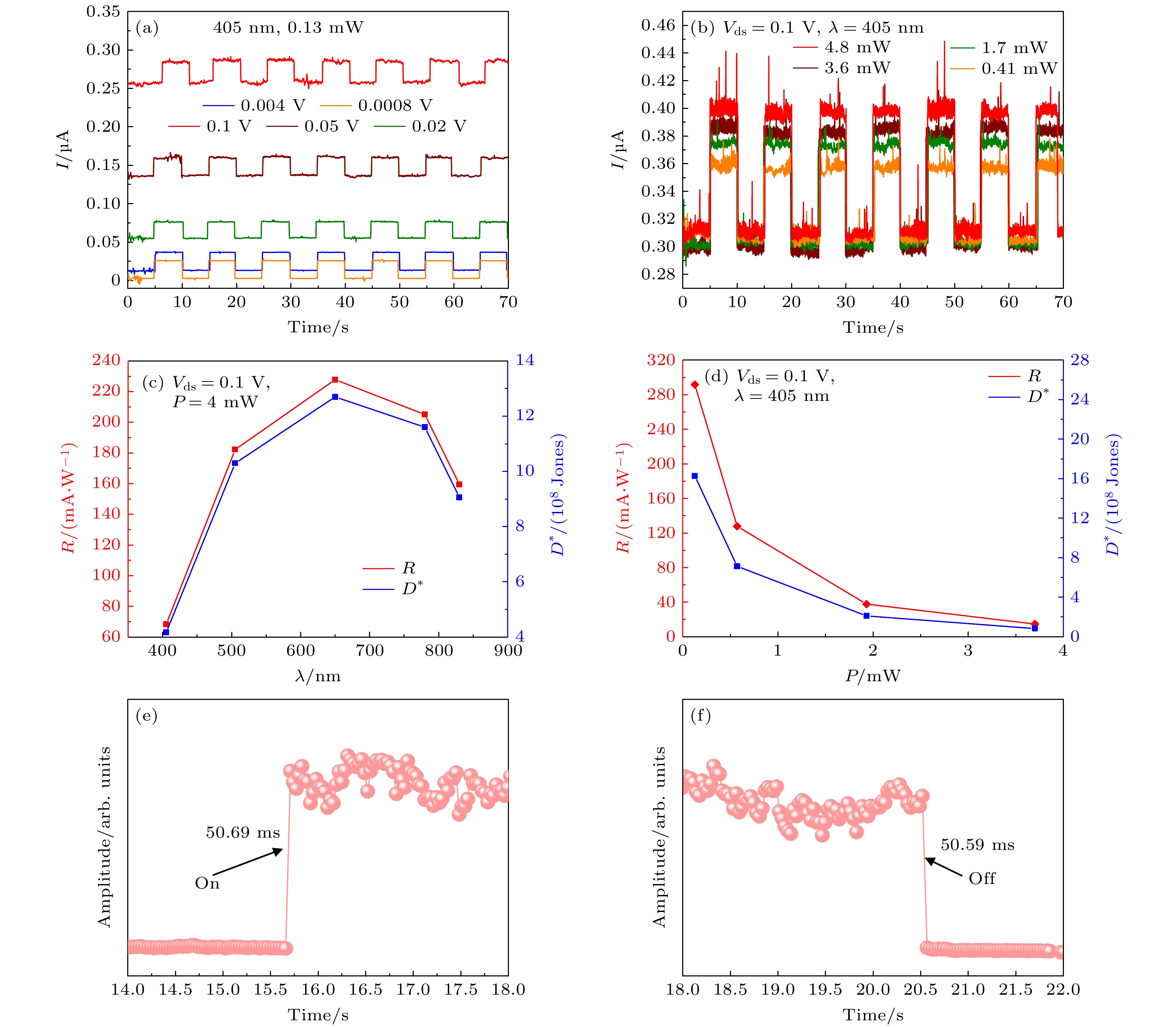
图 5 不同电压(a)和光功率(b)条件的电流随时间变化关系; 光电探测器件的响应度和探测率随波长(c)和光功率(d)的变化关系; 器件的响应上升时间(e)和下降恢复时间(f)
Figure 5. The relation of current with time under different voltage conditions (a) and different optical power conditions (b); the relationship between the responsivity and the detection rate of the photodetector with wavelength (c) and with optical power (d); the rise time (e) and the recovery time (f) of the photodetector.
-
[1] Gao G Y, Yu J, Yang X X, Pang Y K, Zhao J, Pan C F, Sun Q J, Wang Z L 2018 Adv. Mater. 31 1806905
[2] Li X F, Yang L M, Si M W, Li S C, Huang M Q, Ye P D, Wu Y Q 2015 Adv. Mater. 27 1547
Google Scholar
[3] Radisavljevic B, Radenovic A, Brivio J, Giacometti V, Kis A 2011 Nat. Nanotechnol. 6 147
Google Scholar
[4] Kaushik V, Ahmad M, Agarwal K, Varandani D, Belle B D, Das P, Mehta B R 2020 J. Phys. Chem. C 124 23368
Google Scholar
[5] Bagot P A J, Silk O B W, Douglas J O, Pedrazzini S, Crudden D J, Martin T L, Hardy M C, Moody M P, Reed R C 2017 Acta Mater. 125 156
Google Scholar
[6] Wang X D, Wang P, Wang J L, Hu W D, Zhou X H, Guo N, Huang H, Sun S, Shen H, Lin T, Tang M H, Liao L, Jiang A Q, Sun J L, Meng X J, Chen X S, Lu W, Chu J H 2015 Adv. Mater. 27 6575
Google Scholar
[7] Huang Z Z, Zhang T F, Liu J K, Zhang L H, Jin Y H, Wang J P, Jiang K, Fan S, Li Q Q 2019 ACS Appl. Electron. Mater. 1 1314
Google Scholar
[8] Furchi M M, Polyushkin D K, Pospischil A, Mueller T 2014 Nano Lett. 14 6165
Google Scholar
[9] Lee J, Pak S, Lee Y W, Cho Y, Hong J, Giraud P, Shin H S, Morris S M, Sohn J I, Cha S, Kim J M 2017 Nat. Commun. 8 14734
Google Scholar
[10] Lee D, Hwang E, Lee Y, Choi Y, Kim J S, Lee S, Cho J H 2016 Adv. Mater. 28 9196
Google Scholar
[11] Choi M S, Lee G H, Yu Y J, Lee D Y, Lee S H, Kim P, Hone J, Yoo W J 2013 Nat. Commun. 4 1624
Google Scholar
[12] Chen Y F, Wang Y, Wang Z, Gu Y, Ye Y, Chai X L, Ye J F, Chen Y, Xie R Z, Zhou Y, Hu Z G, Li Q, Zhang L L, Wang F, Wang P, Miao J S, Wang J L, Chen X S, Lu W, Zhou P, Hu W D 2021 Nat. Electron. 4 357
Google Scholar
[13] Wu P S, Ye L, Tong L, Wang P, Wang Y, Wang H L, Ge H N, Wang Z, Gu Y, Zhang K, Yu Y Y, Peng M, Wang F, Huang M, Zhou P, Hu W D 2022 Light Sci. Appl. 11 6
Google Scholar
[14] Van Der Zande A M, Huang P Y, Chenet D A, Berkelbach T C, You Y, Lee G H, Heinz T F, Reichman D R, Muller D A, Hone J C 2013 Nat. Mater. 12 554
Google Scholar
[15] Lee H S, Min S W, Chang Y G, Park M K, Nam T, Kim H, Kim J H, Ryu S, Im S 2012 Nano Lett. 12 3695
Google Scholar
[16] Mak K F, Lee C, Hone J, Shan J, Heinz T F 2010 Phys. Rev. Lett. 105 136805
Google Scholar
[17] Li H, Wu J B, Ran F R, Lin M L, Liu X L, Zhao Y Y, Lu X, Xiong Q H, Zhang J, Huang W, Zhang H, Tan P H 2017 ACS Nano 11 11714
Google Scholar
[18] Novoselov K S, Geim A K, Morozov S V, Jiang D, Zhang Y, Dubonos S V, Grigorieva I V, Firsov A A 2004 Science 306 666
Google Scholar
[19] Wang L, Meric I, Huang P Y, Gao Q, Gao Y, Tran H, Taniguchi T, Watanabe K, Campos L M, Muller D A, Guo J, Kim P, Hone J, Shepard K L, Dean C R 2013 Science 342 614
Google Scholar
[20] Yi M, Shen Z G 2015 J. Mater. Chem. A 3 11700
Google Scholar
[21] Ren S, Rong P, Yu Q 2018 Ceramics Int. 44 11940
Google Scholar
[22] Withers F, Yang H, Britnell L, Rooney A P, Lewis E, Felten A, Woods C R, Sanchez Romaguera V, Georgiou T, Eckmann A, Kim Y J, Yeates S G, Haigh S J, Geim A K, Novoselov K S, Casiraghi C 2014 Nano Lett. 14 3987
Google Scholar
[23] Dean C R, Young A F, Meric I, Lee C, Wang L, Sorgenfrei S, Watanabe K, Taniguchi T, Kim P, Shepard K L, Hone J 2010 Nat. Nanotechnol. 5 722
Google Scholar
[24] Sharma M, Singh A, Aggarwal P, Singh R 2022 ACS Omega 7 11731
Google Scholar
[25] Fu D, Zhao X, Zhang Y Y, Li L, Xu H, Jang A R, Yoon S I, Song P, Poh S M, Ren T 2017 J. Am. Chem. Soc. 139 9392
Google Scholar
[26] Lee C H, Zhang Y, Johnson J M, Koltun R, Gambin V, Jamison J S, Myers R C, Hwang J, Rajan S 2020 Appl. Phys. Lett. 117 123102
Google Scholar
[27] Jie W J, Yang Z B, Zhang F, Bai G X, Leung C W, Hao J H 2017 ACS Nano 11 6950
Google Scholar
[28] Kodu M, Avarmaa T, Jaaniso R, Leemets K, Mändar H, Nagirnyi V 2016 Superlattices Microstruct. 98 18
Google Scholar
[29] Wang J, Fan L, Wang X M, Xiao T T, Peng L P, Wang X M, Yu J, Cao L H, Xiong Z W, Fu Y J, Wang C B, Shen Q, Wu W D 2019 Appl. Surf. Sci. 494 651
Google Scholar
[30] Gong Y J, Lin J H, Wang X L, Shi G, Lei S D, Lin Z, Zou X L, Ye G L, Vajtai R, Yakobson B I, Terrones H, Terrones M, Tay B K, Lou J, Pantelides S T, Liu Z, Zhou W, Ajayan P M 2014 Nat. Mater. 13 1135
Google Scholar
[31] Hu S, Wang X F, Meng L, Yan X 2017 J. Mater. Sci. 52 7215
Google Scholar
[32] Liu P Y, Luo T, Xing J, Xu H, Hao H Y, Liu H, Dong J J 2017 Nanoscale Res. Lett. 12 558
Google Scholar
[33] Li M G, Yao J D, Wu X X, Zhang S C, Xing B R, Niu X Y, Yan X Y, Yu Y, Liu Y L, Wang Y W 2020 ACS Appl. Mater. Interfaces 12 6276
Google Scholar
[34] Li J, Yang X D, Liu Y, Huang B L, Wu R X, Zhang Z W, Zhao B, Ma H F, Dang W Q, Wei Z, Wang K, Lin Z Y, Yan X X, Sun M Z, Li B, Pan X Q, Luo J, Zhang G Y, Liu Y, Huang Y, Duan X D, Duan X F 2020 Nature 579 368
Google Scholar
[35] Zhang Z W, Huang Z W, Li J, Wang D, Lin Y, Yang X D, Liu H, Liu S, Wang Y L, Li B, Duan X F, Duan X D 2022 Nat. Nanotechnol. 17 493
Google Scholar
[36] Lopez-Sanchez O, Lembke D, Kayci M, Radenovic A, Kis A 2013 Nat. Nanotechnol. 8 497
Google Scholar
[37] Zhang W, Huang J K, Chen C H, Chang Y H, Cheng Y J, Li L J 2013 Adv. Mater. 25 3456
Google Scholar
[38] Di Bartolomeo A, Genovese L, Foller T, Giubileo F, Luongo G, Croin L, Liang S J, Ang L K, Schleberger M 2017 Nanotechnology 28 214002
Google Scholar
[39] Nie C B, Yu L Y, Wei X Z, Shen J, Lu W Q, Chen W M, Feng S L, Shi H F 2017 Nanotechnology 28 275203
Google Scholar
[40] Han P, St Marie L, Wang Q X, Quirk N, El Fatimy A, Ishigami M, Barbara P 2018 Nanotechnology 29 20LT01
Google Scholar
[41] Pak Y, Park W, Mitra S, Sasikala Devi A A, Loganathan K, Kumaresan Y, Kim Y, Cho B, Jung G Y, Hussain M M, Roqan I S 2018 Small 14 201703176
[42] Radisavljevic B, Kis A 2013 Nat. Mater. 12 815
Google Scholar
[43] Wang J, Yao Q, Huang C W, Zou X, Liao L, Chen S, Fan Z, Zhang K, Wu W, Xiao X, Jiang C, Wu W W 2016 Adv. Mater. 28 8302
Google Scholar
[44] Li Y N, Li L N, Li S S, Sun J Y, Fang Y, Deng T 2022 ACS Omega 7 13615
Google Scholar
[45] Zhao T G, Guo J X, Li T T, Wang Z, Peng M, Zhong F, Chen Y, Yu Y Y, Xu T F, Xie R Z, Gao P Q, Wang X R, Hu W D 2023 Chem. Soc. Rev. 52 1650
Google Scholar
[46] Suleman M, Lee S, Kim M, Nguyen V H, Riaz M, Nasir N, Kumar S, Park H M, Jung J, Seo Y 2022 ACS Omega 7 30074
Google Scholar
[47] Sun P, Liu Y W, Ma J, Li W, Zhang K L, Yuan Y J 2019 CrystEngComm 21 6969
Google Scholar
[48] Zhao T G, Zhong F, Wang S C, Wang Y K, Xu T F, Chen Y, Yu Y Y, Guo J X, Wang Z, Yu J C, Gao P Q 2022 Adv. Opt. Mater. 11 2202208
[49] Sinha S, Kumar S, Arora SK, Sharma A, Tomar M, Wu H C, Gupta V 2021 J. Appl. Phys. 129 155304
Google Scholar

 DownLoad:
Catalog
Metrics
- Abstract views: 2243
- PDF Downloads: 75
- Cited By: 0
