


-
Molybdenum disulfide (MoS2), as a kind of two-dimensional(2D) material with novel physical properties and excellent electrical performances, has great potential applications in electronic devices. Efficient and controllable growth of large-size single crystal MoS2 is a major difficulty that must be overcome towards scalable production. Chemical vapor deposition (CVD) is considered as the most promising means for industrial production of 2D materials. Here in this work, the high-quality and millimeter-level single crystal MoS2monolayer grows on molten glass by the pre-chemical vapor deposition, in which MoO3 film deposited on the molten glass is used as Mo precursor instead of MoO3 powder. In addition, by introducing WO3 powder into such a CVD system, MoS2-WS2 lateral heterojunctions can also be obtained. Raman and PL measurements indicate that the as-grown MoS2 monolayer samples possess high quality. The Back-gate FETs are fabricated on SiO2/Si substrates by using transferring elelctrode methods to investigate the electrical properties of the as-grown MoS2 crystals. At room temperature and atmosphere pressure, the on-off ratio can reach 105 and the carrier mobility can arrive at 4.53 cm2/(V·s). The low-cost and high-quality large-size material growth method pave the way for the scalable production of such a 2D material based electronic devices.
-
Keywords:
- MoS2 /
- molten glass /
- CVD /
- heterojunction
[1] Hynek D J, Singhania R M, Xu S, Davis B, Wang L, Yarali M, Pondick J V, Woods J M, Strandwitz N C, Cha J J 2021 ACS Nano 15 410
 Google Scholar
[2] Susarla S, Kutana A, Hachtel J A, Kochat V, Apte A, Vajtai R, Idrobo J C, Yakobson B I, Tiwary C S, Ajayan P M 2017 Advan. Mater. 29 1702457
Google Scholar
[3] Huo N, Yang Y, Li J 2017 J. Semicond. 38 031002
Google Scholar
[4] Cheng P, Tang C, Ahmed S, Qiao J, Zeng L, Tsang Y 2020 Nanotechnology 32 055201
[5] Wu Y, Lin Y M, Bol A A, Jenkins K A, Xia F, Farmer D B, Zhu Y, Avouris P 2011 Nature 472 74
Google Scholar
[6] Sarkar D, Xie X, Liu W, Cao W, Kang J, Gong Y, Kraemer S, Ajayan P M, Banerjee K 2015 Nature 526 91
Google Scholar
[7] Jia S, Jin Z, Zhang J, Yuan J, Chen W, Feng W, Hu P, Ajayan P M, Lou J 2020 Small 16 2002263
Google Scholar
[8] Akinwande D, Petrone N, Hone J 2014 Nat. Commun. 5 5678
Google Scholar
[9] Chang H Y, Yang S, Lee J, Tao L, Hwang W S, Jena D, Lu N, Akinwande D 2013 ACS Nano 7 5446
Google Scholar
[10] Lee G H, Yu Y J, Cui X, Petrone N, Lee C H, Choi M S, Lee D Y, Lee C, Yoo W J, Watanabe K, Taniguchi T, Nuckolls C, Kim P, Hone J 2013 ACS Nano 7 7931
Google Scholar
[11] Das S, Gulotty R, Sumant A V, Roelofs A 2014 Nano Lett. 14 2861
Google Scholar
[12] Xiao X, Chen M, Zhang J, Zhang T, Zhang L, Jin Y, Wang J, Jiang K, Fan S, Li Q 2019 ACS Appl. Mater. Inter. 11 11612
Google Scholar
[13] 董艳芳, 何大伟, 王永生, 许海腾, 巩哲 2016 物理学报 65 128101
Google Scholar
Dong Y F, He D W, Wang Y S, Xu H T, Gong Z 2016 Acta Phys. Sin. 65 128101
Google Scholar
[14] 王铄, 王文辉, 吕俊鹏, 倪振华 2021 物理学报 70 026802
Wang S, Wang W H, Lv J P, Ni Z H 2021 Acta Phys. Sin. 70 026802
[15] Yang P, Zou X, Zhang Z, Hong M, Shi J, Chen S, Shu J, Zhao L, Jiang S, Zhou X, Huan Y, Xie C, Gao P, Chen Q, Zhang Q, Liu Z, Zhang Y 2018 Nat. Commun. 9 979
Google Scholar
[16] Zhang Z, Xu X, Song J, Gao Q, Li S, Hu Q, Li X, Wu Y 2018 Appl. Phys. Lett. 113 202103
Google Scholar
[17] Chen J, Zhao X, Tan S J R, Xu H, Wu B, Liu B, Fu D, Fu W, Geng D, Liu Y, Liu W, Tang W, Li L, Zhou W, Sum T C, Loh K P 2017 J. Am. Chem. Soc. 139 1073
Google Scholar
[18] Tang L, Tan J, Nong H, Liu B, Cheng H M 2021 Acc. Mater. Res. 2 36
Google Scholar
[19] Wan X, Miao X, Yao J, Wang S, Shao F, Xiao S, Zhan R, Chen K, Zeng X, Gu X, Xu J 2021 Advan. Mater. 33 2100260
Google Scholar
[20] Zhang X, Nan H, Xiao S, Wan X, Gu X, Du A, Ni Z, Ostrikov K 2019 Nat. Commun. 10 598
Google Scholar
[21] Wang Z, Xie Y, Wang H, Wu R, Nan T, Zhan Y, Sun J, Jiang T, Zhao Y, Lei Y, Yang M, Wang W, Zhu Q, Ma X, Hao Y 2017 Nanotechnology 28 325602
Google Scholar
[22] Park J H, Lu A Y, Shen P C, Shin B G, Wang H, Mao N, Xu R, Jung S J, Ham D, Kern K, Han Y, Kong J 2021 Small Methods 5 2000720
Google Scholar
[23] 王璐, 高俊峰, 丁峰 2014 化学学报 72 345
Google Scholar
Wang L, Gao J F, Ding F 2014 Acta Chim. Sin. 72 345
Google Scholar
[24] Wang J, Cai X, Shi R, Wu Z, Wang W, Long G, Tang Y, Cai N, Ouyang W, Geng P, Chandrashekar B N, Amini A, Wang N, Cheng C 2018 ACS Nano 12 635
Google Scholar
[25] Yang P, Zhang S, Pan S, Tang B, Liang Y, Zhao X, Zhang Z, Shi J, Huan Y, Shi Y, Pennycook S J, Ren Z, Zhang G, Chen Q, Zou X, Liu Z, Zhang Y 2020 ACS Nano 14 5036
Google Scholar
[26] Withanage S S, Khondaker S I 2019 MRS Advan. 4 587
Google Scholar
-
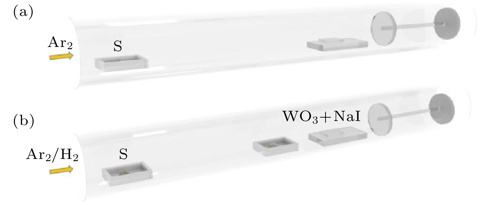
图 1 (a)生长MoS2的实验装置示意图; (b)生长WS2-MoS2的实验装置示意图
Figure 1. Schematic illustrations of the experimental set-up for (a) MoS2 and (b) MoS2-WS2 heterostructure.

图 2 (a)熔融玻璃衬底上CVD过程的示意图; (b)尺寸500 μm的MoS2的光镜图; (c)毫米级的MoS2的光镜图
Figure 2. (a) Schematic illustration of CVD reaction process of the as-grown MoS2 films on the soda-lime glass; (b) optical images of MoS2 with size of 500 μm, (c) optical images of MoS2 with size of 1 mm.

图 3 转移至硅衬底上的MoS2及相应的拉曼荧光表征 (a)(b)转移后的MoS2光镜图; (c)(d)为(b)中样品的拉曼与荧光表征; (e)所生长MoS2的AFM图像; (f)生长MoS2的HRTEM, 内插图为相应的SAED
Figure 3. MoS2 films transfered onto the Si/SiO2 substrates and its Raman spectrum: (a) (b) Optical images of transfered MoS2; (c) (d)single-point Raman and PL spectrum of the as-grown MoS2films in (b); (e) AFM image of as-grown MoS2; (f) HRTEM of as-grown MoS2, the inset image is the SAED pattern of as-grown MoS2.
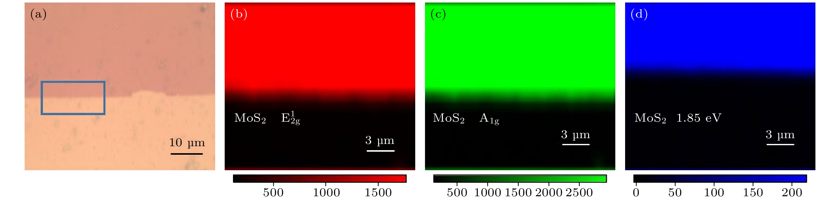
图 4 所生长MoS2薄膜的拉曼与荧光 mapping测试(a) MoS2薄膜光镜图; (b)图(a)中蓝框区域拉曼峰
$ \rm E^1_{\rm 2g} $ 的mapping图像; (c)拉曼峰A1g的mapping图像; (d)荧光峰1.85 eV处的mapping图像Figure 4. Raman mapping test of as-grown MoS2 film: (a) Optical image of a selected MoS2 films; (b) Raman intensity mapping of
$ \rm E^1_{\rm 2g} $ peak (blue area in Fig. (a)); (c) Raman intensity mapping of A1g (blue area in Fig. (a)) ; (d) PL intensity mapping of PL peak at 1.85 eV (blue area in Fig. (a)).
图 5 (a) MoS2场效应管的3D模型以及真实器件的光镜图; (b) MoS2场效应管的输出曲线; (c) MoS2场效应管的线性转移曲线; (d) MoS2场效应管的指数转移曲线
Figure 5. (a) Schematic of MoS2 FET and a typical optical image of the devices; (b) output curves (Ids-Vds) of a typical MoS2 FET device; (c) liner transfer curves of a typical MoS2 FET device; (d) semilog transfer curves of a typical MoS2 FET device.
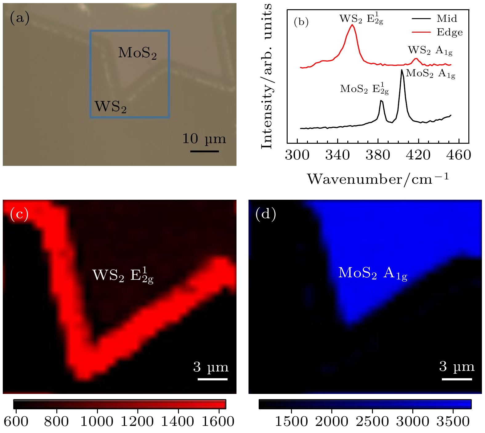
图 6 (a)熔融玻璃上生长的WS2-MoS2异质结的光镜图; (b) WS2-MoS2相应区域的拉曼表征; (c)异质结对应于350 cm–1处的拉曼强度mapping; (d)异质结对应于403 cm–1处的拉曼强度mapping
Figure 6. (a) Optical image of the as-grown WS2-MoS2 heterostructures on soda-lime glass; (b) single-point Raman spectra of the as-grown WS2-MoS2 heterostructures, (c) Raman intensity mapping of the heterostructure region at 350 cm–1; (d) Raman intensity mapping of the heterostructure region at 403 cm–1.
-
[1] Hynek D J, Singhania R M, Xu S, Davis B, Wang L, Yarali M, Pondick J V, Woods J M, Strandwitz N C, Cha J J 2021 ACS Nano 15 410
Google Scholar
[2] Susarla S, Kutana A, Hachtel J A, Kochat V, Apte A, Vajtai R, Idrobo J C, Yakobson B I, Tiwary C S, Ajayan P M 2017 Advan. Mater. 29 1702457
Google Scholar
[3] Huo N, Yang Y, Li J 2017 J. Semicond. 38 031002
Google Scholar
[4] Cheng P, Tang C, Ahmed S, Qiao J, Zeng L, Tsang Y 2020 Nanotechnology 32 055201
[5] Wu Y, Lin Y M, Bol A A, Jenkins K A, Xia F, Farmer D B, Zhu Y, Avouris P 2011 Nature 472 74
Google Scholar
[6] Sarkar D, Xie X, Liu W, Cao W, Kang J, Gong Y, Kraemer S, Ajayan P M, Banerjee K 2015 Nature 526 91
Google Scholar
[7] Jia S, Jin Z, Zhang J, Yuan J, Chen W, Feng W, Hu P, Ajayan P M, Lou J 2020 Small 16 2002263
Google Scholar
[8] Akinwande D, Petrone N, Hone J 2014 Nat. Commun. 5 5678
Google Scholar
[9] Chang H Y, Yang S, Lee J, Tao L, Hwang W S, Jena D, Lu N, Akinwande D 2013 ACS Nano 7 5446
Google Scholar
[10] Lee G H, Yu Y J, Cui X, Petrone N, Lee C H, Choi M S, Lee D Y, Lee C, Yoo W J, Watanabe K, Taniguchi T, Nuckolls C, Kim P, Hone J 2013 ACS Nano 7 7931
Google Scholar
[11] Das S, Gulotty R, Sumant A V, Roelofs A 2014 Nano Lett. 14 2861
Google Scholar
[12] Xiao X, Chen M, Zhang J, Zhang T, Zhang L, Jin Y, Wang J, Jiang K, Fan S, Li Q 2019 ACS Appl. Mater. Inter. 11 11612
Google Scholar
[13] 董艳芳, 何大伟, 王永生, 许海腾, 巩哲 2016 物理学报 65 128101
Google Scholar
Dong Y F, He D W, Wang Y S, Xu H T, Gong Z 2016 Acta Phys. Sin. 65 128101
Google Scholar
[14] 王铄, 王文辉, 吕俊鹏, 倪振华 2021 物理学报 70 026802
Wang S, Wang W H, Lv J P, Ni Z H 2021 Acta Phys. Sin. 70 026802
[15] Yang P, Zou X, Zhang Z, Hong M, Shi J, Chen S, Shu J, Zhao L, Jiang S, Zhou X, Huan Y, Xie C, Gao P, Chen Q, Zhang Q, Liu Z, Zhang Y 2018 Nat. Commun. 9 979
Google Scholar
[16] Zhang Z, Xu X, Song J, Gao Q, Li S, Hu Q, Li X, Wu Y 2018 Appl. Phys. Lett. 113 202103
Google Scholar
[17] Chen J, Zhao X, Tan S J R, Xu H, Wu B, Liu B, Fu D, Fu W, Geng D, Liu Y, Liu W, Tang W, Li L, Zhou W, Sum T C, Loh K P 2017 J. Am. Chem. Soc. 139 1073
Google Scholar
[18] Tang L, Tan J, Nong H, Liu B, Cheng H M 2021 Acc. Mater. Res. 2 36
Google Scholar
[19] Wan X, Miao X, Yao J, Wang S, Shao F, Xiao S, Zhan R, Chen K, Zeng X, Gu X, Xu J 2021 Advan. Mater. 33 2100260
Google Scholar
[20] Zhang X, Nan H, Xiao S, Wan X, Gu X, Du A, Ni Z, Ostrikov K 2019 Nat. Commun. 10 598
Google Scholar
[21] Wang Z, Xie Y, Wang H, Wu R, Nan T, Zhan Y, Sun J, Jiang T, Zhao Y, Lei Y, Yang M, Wang W, Zhu Q, Ma X, Hao Y 2017 Nanotechnology 28 325602
Google Scholar
[22] Park J H, Lu A Y, Shen P C, Shin B G, Wang H, Mao N, Xu R, Jung S J, Ham D, Kern K, Han Y, Kong J 2021 Small Methods 5 2000720
Google Scholar
[23] 王璐, 高俊峰, 丁峰 2014 化学学报 72 345
Google Scholar
Wang L, Gao J F, Ding F 2014 Acta Chim. Sin. 72 345
Google Scholar
[24] Wang J, Cai X, Shi R, Wu Z, Wang W, Long G, Tang Y, Cai N, Ouyang W, Geng P, Chandrashekar B N, Amini A, Wang N, Cheng C 2018 ACS Nano 12 635
Google Scholar
[25] Yang P, Zhang S, Pan S, Tang B, Liang Y, Zhao X, Zhang Z, Shi J, Huan Y, Shi Y, Pennycook S J, Ren Z, Zhang G, Chen Q, Zou X, Liu Z, Zhang Y 2020 ACS Nano 14 5036
Google Scholar
[26] Withanage S S, Khondaker S I 2019 MRS Advan. 4 587
Google Scholar

 DownLoad:


Catalog
Metrics
- Abstract views: 4113
- PDF Downloads: 126
- Cited By: 0
