


-
As the substance carrier of nonlinear optical phenomenon, saturable absorber is an essential material for generating the ultrafast pulse laser. The saturable absorbers based on graphene, transition metal sulfides, topological insulators, black phosphorus and other two-dimensional (2D) materials exhibit different optical advantages. However, limitations of those single 2D materials as saturable absorbers exist. The nanomaterial heterojunction structure can combine the advantages of different 2D materials to achieve optical complementarity, and it also provides new ideas for generating the ultrafast laser with ultrashort pulse duration and high peak power. Here in this paper, the preparation methods, band alignment and the electronic transition mechanism of heterojunction saturable absorbers are summarized, and the recent research progress of ultrafast lasers based on 2D nano-heterostructures are also reviewed, including the wavelength, pulse width, repetition frequency and pulse energy. Therefore, 2D nano-heterostructure exhibits great potential applications in future optical modulator and optical switch.
-
Keywords:
- two-dimensional materials /
- heterostructure /
- saturable absorber /
- ultrafast laser
[1] Wu L, Huang W, Wang Y, Zhao J, Ma D, Xiang Y, Li J, Ponraj J S, Dhanabalan S C, Zhang H 2019 Adv. Funct. Mater. 29 1806346
 Google Scholar
[2] Jia Y, Liao Y, Wu L, Shan Y, Dai X, Cai H, Xiang Y, Fan D 2019 Nanoscale 11 4515
Google Scholar
[3] Russo R E, Mao X, Haichen L, Gonzalez J J, Mao S S 2002 Talanta 57 425
Google Scholar
[4] Rea R, Di Matteo F M, Martino M, Pandolfi M, Saccomandi P, Rabitti C, Crescenzi A, Costamagna G 2017 Lasers Med. Sci. 32 1411
Google Scholar
[5] Kalisky Y, Kalisky O 2011 Opt. Mater. 34 457
Google Scholar
[6] Malinauskas M, Albertas Ž, Hasegawa S, Hayasaki Y, Mizeikis V, Juodkazis S 2016 Light-Sci. Appl. 5 16133
Google Scholar
[7] Woodward R, Kelleher E 2015 Appl. Sci. 5 1440
Google Scholar
[8] Okhotnikov O, Grudinin A, Pessa M 2004 New J. Phys. 6 177
Google Scholar
[9] Tang C Y, Cheng P K, Tao L, Long H, Zeng L H, Wen Q, Tsang Y H 2017 J. Light Technol. 35 4120
Google Scholar
[10] Bao Q, Zhang H, Wang Y, Ni Z, Yan Y, Shen Z X, Loh K P, Tang D Y 2009 Adv. Funct. Mater. 19 3077
Google Scholar
[11] Xu J L, Li X L, Wu Y Z, Hao X P, He J L, Yang K J 2011 Opt. Lett. 36 1948
Google Scholar
[12] 王聪, 刘杰, 张晗 2019 物理学报 68 188101
Google Scholar
Wang C, Liu J, Zhang H 2019 Acta Phys. Sin. 68 188101
Google Scholar
[13] 张倩, 金鑫, 张梦, 郑铮 2020 物理学报 69 188101
Google Scholar
Zhang Q, Jin X X, Zhang M, Zheng Z 2020 Acta Phys. Sin. 69 188101
Google Scholar
[14] Long H, Tang C Y, Cheng P K, Wang X Y, Qarony W, Tsang Y H 2019 J. Lightwave Technol. 37 1174
Google Scholar
[15] Long H, Shi Y, Wen Q, Tsang Y H 2019 J. Mater. Chem. C 7 5937
Google Scholar
[16] He J, Tao L, Zhang H, Zhou B, Li J 2019 Nanoscale 11 2577
Google Scholar
[17] Tao L, Huang X, He J, Lou Y, Zeng L, Li Y, Long H, Li J, Zhang L, Tsang Y H 2018 Photonics Res. 6 750
Google Scholar
[18] Yu H, Zheng X, Yin K, Cheng X, Jiang T 2015 Appl. Opt. 54 10290
Google Scholar
[19] Luo Z, Huang Y, Zhong M, Li Y, Wu J, Xu B, Xu H, Cai Z, Peng J, Weng J 2014 J. Lightwave Technol. 32 4077
[20] Yan P, Liu A, Chen Y, Wang J, Ruan S, Chen H, Ding J 2015 Sci. Rep. 5 12587
Google Scholar
[21] Luo Z C, Liu M, Guo Z N, Jiang X F, Luo A P, Zhao C J, Yu X F, Xu W C, Zhang H 2015 Opt. Express 23 20030
Google Scholar
[22] Ming N, Tao S, Yang W, Chen Q, Sun R, Wang Ch, Wang S, Man B, Zhang H 2018 Opt. Express 26 9017
Google Scholar
[23] Lee Y W, Chen C M, Huang C W, Chen S K, Jiang J R 2016 Opt. Express 24 10675
Google Scholar
[24] Sun Z, Hasan T, Torrisi F, Popa D, Privitera G, Wang F, Bonaccorso F, Basko D M, Ferrari A C 2010 ACS Nano 4 803
Google Scholar
[25] Chen Y, Jiang G, Chen S, Guo Z, Yu X, Zhao C, Zhang H, Bao Q, Wen S, Tang D, Fan D 2015 Opt. Express 23 12823
Google Scholar
[26] Wang Y, Lee P, Zhang B, Sang Y, He J 2017 Nanoscale 9 19100
Google Scholar
[27] Jiang X, Liu S, Liang W, Luo S, He Z, Ge Y, Wang H, Cao R, Zhang F, Wen Q, Li J, Bao Q 2017 Laser Photonics Rev. 12 1700229
Google Scholar
[28] Wang Y, Huang G, Mu H, Lin S, Chen J, Xiao S, Bao Q, He J 2015 Appl. Phys. Lett. 107 091905
Google Scholar
[29] Geim A K, Grigorieva I V 2013 Nature 499 419
Google Scholar
[30] Liu L, Chu H, Zhang X, Pan H, Zhao S, Li D 2019 Nanoscale Res. Lett. 14 112
Google Scholar
[31] Zhang H, Zhang F, Li X, Chen L, Wang J, Wang L 2017 Opt. Mater. 70 153
Google Scholar
[32] Li Z, Cheng C, Dong N, Romero C, Lu Q, Wang J, Rodríguez Vázquez de Aldana J, Tan Y, Chen F 2017 Photonics Res. 5 406
Google Scholar
[33] You Z, Sun Y, Sun D, Zhu Z, Wang Y, Li J, Tu C, Xu J 2017 Opt. Lett. 42 871
Google Scholar
[34] Wen Y, Zhao X S, Zhang W 2018 Optik 170 90
Google Scholar
[35] Zhao G, Lv X, Xie Z, Xu J 2017 Conference on Lasers and Electro-Optics Pacific Rim (CLEO-PR) Singapore, July 31−Aug 4, 2017 p1
[36] Stankovich S, Dikin D A, Dommett G H B, Kohlhaas K M, Zimney E J, Stach E A, Piner R D, Nguyen S T, Ruoff R S 2006 Nature 442 282
Google Scholar
[37] He J, Wang C, Zhou B, Zhao Y, Tao L, Zhang H 2020 Mater. Horiz.
Google Scholar
[38] Novoselov K S, Geim A K, Morozov S V, Jiang D, Zhang Y, Dubonos S V, Grigorieva I V, Firsov A A 2004 Science 306 666
Google Scholar
[39] Wu J, Li H, Yin Z, Li H, Liu J, Cao X, Zhang Q, Zhang H 2013 Small 9 3314
Google Scholar
[40] Pezeshki A, Shokouh S H H, Nazari T, Oh K, Im S 2016 Adv. Mater. 28 3216
Google Scholar
[41] Wang W, Chen S J, Basquiroto de Souza F, Wu B, Duan W H 2018 Nanoscale 10 1004
Google Scholar
[42] Lu L, Liang Z, Wu L, Chen Y X, Song Y, Dhanabalan S C, Ponraj J S, Dong B, Xiang Y, Xing F, Fan D, Zhang H 2018 Laser Photonics Rev. 12 1700221
Google Scholar
[43] Kim J, Kwon S, Cho D H, Kang B, Kwon H, Kim Y, Park S O, Jung G Y, Shin E, Kim W G, Lee H, Ryu G H, Choi M, Kim T H, Oh J, Park S, Kwak S K, Yoon S W, Byun D, Lee Z, Lee C 2015 Nat. Commun. 6 8294
Google Scholar
[44] Tao L, Long H, Zhou B, Yu S F, Lau S P, Chai Y, Fung K H, Tsang Y H, Yao J, Xu D 2014 Nanoscale 6 9713
Google Scholar
[45] Shi Y, Long H, Liu S, Tsang Y H, Wen Q 2018 J. Mater. Chem. C 6 12638
Google Scholar
[46] Lu C, Quan C, Si K, Xu X, He C, Zhao Q, Zhan Y, Xu X 2019 Appl. Surf. Sci. 479 1161
Google Scholar
[47] Quan C, Lu C, He C, Xu X, Huang Y, Zhao Q, Xu X 2019 Adv. Mater. Interfaces 6 1801733
Google Scholar
[48] Lee Y H, Zhang X Q, Zhang W, Chang M T, Lin C Te, Chang K Di, Yu Y C, Wang J T W, Chang C S, Li L J, Lin T W 2012 Adv. Mater. 24 2320
Google Scholar
[49] Reina A, Jia X, Ho J, Nezich D, Son H, Bulovic V, Dresselhaus M, Jing K, Kong J 2008 Nano Lett. 9 30
Google Scholar
[50] Schmidt H, Wang S, Chu L, Toh M, Kumar R, Zhao W, Neto A H C, Martin J, Adam S, Oezyilmaz B, Eda G 2014 Nano Lett. 14 1909
Google Scholar
[51] Zhan Y, Liu Z, Najmaei S, Ajayan P M, Lou J 2012 Small 8 966
Google Scholar
[52] Cong C, Shang J, Wu X, Cao B, Peimyoo N, Qiu C, Litao S, Yu T 2014 Adv. Opt. Mater. 2 12512
Google Scholar
[53] Hong X, Kim J, Shi S-F, Zhang Y, Jin C, Sun Y, Tongay S, Wu J, Zhang Y, Wang F 2014 Nat. Nanotechnol. 9 682
Google Scholar
[54] Chen H, Wen X, Zhang J, Wu T, Gong Y, Zhang X, Yuan J, Yi C, Lou J, Ajayan P M, Zhuang W, Zhang G, Zheng J 2016 Nat. Commun. 7 1
Google Scholar
[55] Qiao H, Yuan J, Xu Z, Chen C, Lin S, Wang Y, Song J, Liu Y, Khan Q, Hoh H Y, Pan C X, Li S, Bao Q 2015 ACS Nano 9 1886
Google Scholar
[56] Wang Z, Mu H, Yuan J, Zhao C, Bao Q, Zhang H 2017 IEEE J. Sel. Top. Quantum Electron. 23 8800105
Google Scholar
[57] Liu W J, Liu M L, Liu B, Quhe R G, Lei M, Fang S B, Teng H, Wei Z Y 2019 Opt. Express 27 6689
Google Scholar
[58] Lee J, Shin J H, Lee G H, Lee C H 2016 Nanomaterials 6 193
Google Scholar
[59] Velický M, Toth P S 2017 Appl. Mater. Today 8 68
Google Scholar
[60] Liu B, Long M, Cai M Q, Yang J 2018 J. Phys. Chem. Lett. 9 4822
Google Scholar
[61] Niu T, Li A 2015 Prog. Surf. Sci. 90 21
Google Scholar
[62] Ma S, Zeng L, Tao L, Tang C Y, Yuan H, Long H, Cheng P K, Chai Y, Chen C, Fung K H, Zhang X, Lau S P, Tsang Y H 2017 Sci. Rep. 7 3125
Google Scholar
[63] Chen H, Yin J, Yang J, Zhang X, Liu M, Jiang Z, Wang J, Sun Z, Guo T, Liu W, Yan P 2017 Opt. Lett. 42 4279
Google Scholar
[64] Sun X, Zhang B, Li Y, Luo X, Li G, Chen Y, Zhang C, He J 2018 ACS Nano 12 11376
Google Scholar
[65] Yan B, Li G, Shi B, Liu J, Nie H, Yang K, Zhang B, He J 2020 Nanophotonics 9 2593
Google Scholar
[66] 祎然 2019 博士学位论文 (济南: 山东大学)
Wang Y R 2019 Ph. D. Dissertation (Jinan: ShanDong University) (in Chinese)
[67] Zhao G, Hou J, Wu Y, He J, Hao X 2015 Adv. Opt. Mater. 3 937
Google Scholar
[68] Jiang Y, Miao L, Jiang G, Chen Y, Qi X, Jiang X 2015 Sci. Rep. 5 16372
Google Scholar
[69] Du W, Li H, Liu C, Shen S, Liu Y, Lan C, Li C 2017 Proc. SPIE 10457, AOPC 2017: Laser Components, Systems, and Applications Beijing, China, October 24, 2017 104571 M
[70] Mu H, Tuo M, Xu C, Bao X, Xiao S, Sun T, Li L, Zhao L, Li S, Ren W, Bao Q 2019 Opt. Mater. Express 9 3268
Google Scholar
[71] Liu S, Li Z, Ge Y, Wang H, Yue R, Jiang X, Li J, Wen Q, Zhang H 2017 Photonics Res. 5 662
Google Scholar
[72] Mu H, Wang Z, Yuan J, Xiao S, Chen C, Chen Y, Chen Y, Song J, Wang Y, Xue Y, Zhang H, Bao Q 2015 ACS Photonics 2 832
Google Scholar
[73] Zhang L, Liu J, Li J, Wang Z, Wang Y, Ge Y, Dong W, Xu N, He T, Zhang H, Zhang W 2020 Laser Photonics Rev. 14 1900409
Google Scholar
[74] Liu C, Li H, Deng G, Lan C, Li C, Liu Y 2016 2016 Asia Communications and Photonics Conference (ACP) Wuhan, China, Novermber 2−5, 2016 p1
[75] Jiang C, Ning J, Li X, Wang X, Zhang Z 2019 Nanoscale Res. Lett. 14 15252
[76] Song Y, You K, Zhao J, Huang D, Chen Y, Xing C, Zhang H 2020 Nanoscale 12 15252
Google Scholar
[77] Liu W, Zhu Y N, Liu M, Wen B, Fang S, Teng H, Lei M, Liu L M, Wei Z 2018 Photonics Res. 6 220
Google Scholar
[78] Olle V F, Vasil’v P P, Wonfor A, Penty R V, White I H 2012 Opt. Express 20 7035
Google Scholar
[79] Du W, Li H, Lan C, Li C, Li J, Wang Z, Liu Y 2020 Opt. Express 28 11514
Google Scholar
[80] Ma X, Lu B, Qi X, Lu C, Li D, Wen Z, Xu X, Bai J 2019 Appl. Phys. Express 12 112006
Google Scholar
[81] Wang Z, Mu H, Zhao C, Bao Q, Zhang H 2016 Opt. Eng. 55 081314
Google Scholar
[82] Chen H, Li I L, Zhang M, Wang J, Yan P 2017 Opto-Electronics Commun. Conf. OECC 2017 Photonics Glob. Conf. PGC Singapore, July 31−Aug 4, 2017 p1
-
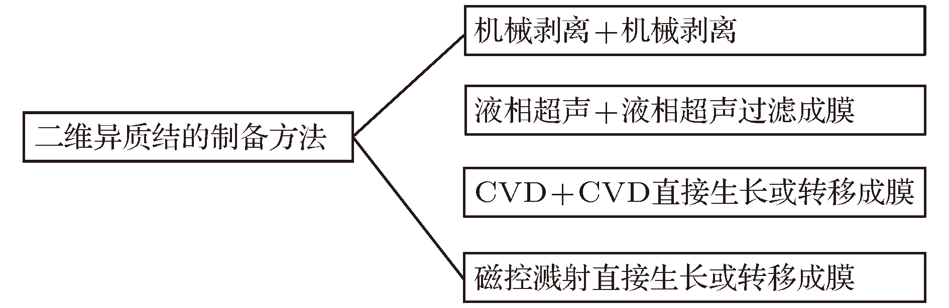
图 1 二维异质结可饱和吸收体主要制备方法
Figure 1. Fabrication methods of two-dimensional heterostructure saturable absorbers.
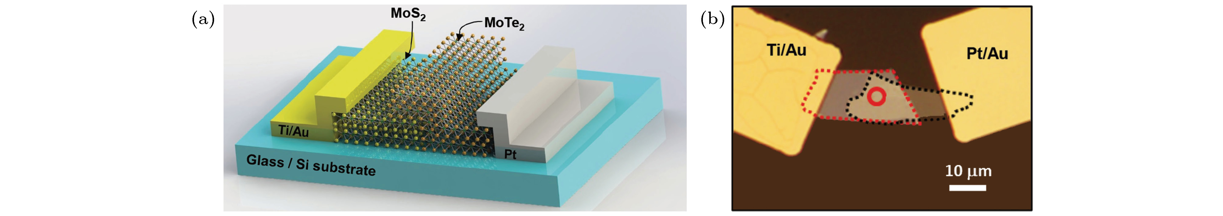
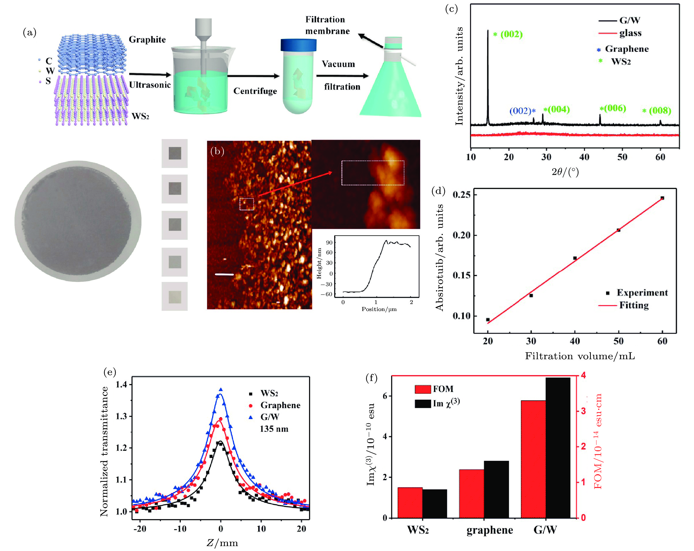
图 3 (a) 液相超声剥离法制备WS2/Graphene异质结流程图及不同掺杂含量对成膜厚度的影响; (b) 异质结原子力显微镜图; (c) X射线衍射图; (d)吸收强度随抽滤体积的变化; (e) WS2, Graphene, 及WS2/Graphene异质结Z-扫描结果; (f) WS2, Graphene, 及WS2/Graphene三阶非线性系数及FOM比较[41]
Figure 3. (a) Illustration of preparation procedures of WS2/Graphene heterostructure films by liquid phase exfoliation, a series of of WS2/Graphene heterostructure films with different thickness obtained from different filtration volume; (b) atomic force microscopy image of WS2/Graphene heterostructure films; (c) X-ray diffraction patterns; (d) absorption as a function of filtration volume at 800 nm; (e) open-aperture Z-scan results of WS2, Graphene, and WS2/Graphene heterostructure films with the thickness of ~135 nm; (f) histogram of the imaginary part of the third-order nonlinear coefficient Imχ(3) and figure of merit (FOM) of WS2, Graphene, and WS2/Graphene heterostructure[41].

图 4 (a)液相超声剥离法制备MoTe2/MoS2异质结流程图及不同掺杂含量对成膜厚度的影响; (b) MoTe2, MoS2, 及MoTe2/MoS2的Z-扫描结果; (c)不同厚度的MoTe2/MoS2异质结薄膜Z-扫描结果[47]
Figure 4. (a) Illustration of preparation procedures of MoTe2/MoS2 heterostructure films by liquid phase exfoliation; (b) Z-scan results of MoTe2, MoS2 and MoTe2/MoS2 heterostructure films under the pump intensity of 606 GW·cm–2 with the thickness of ~80 nm; (c) Z-scan results of MoTe2/MoS2 heterostructure films with thickness of 30, 60, 80, 100, 120 nm at 606 GW·cm–2, respectively[47].
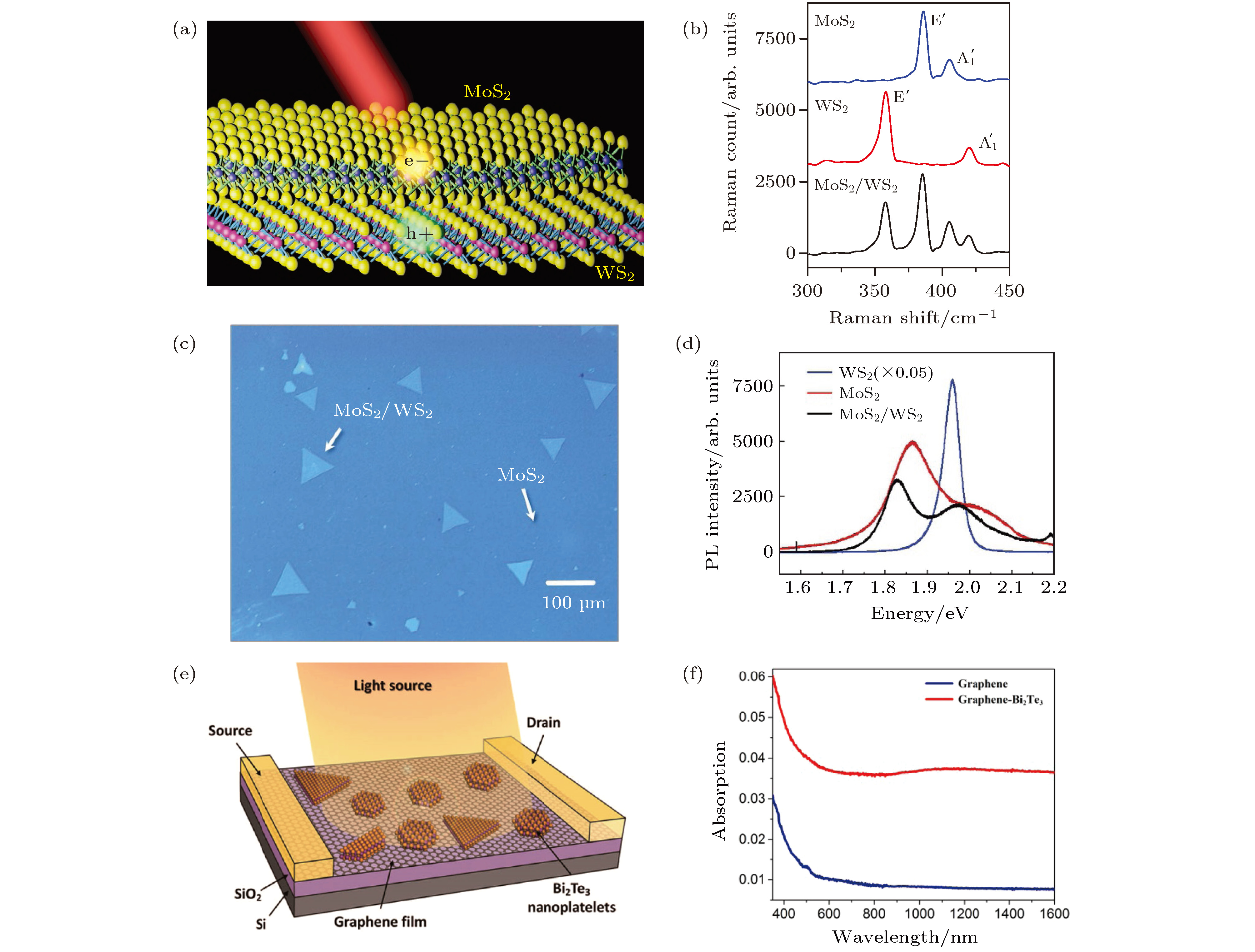
图 5 (a), (b) CVD制备的单层MoS2并转移到单层WS2上组成MoS2/WS2异质结及其特征拉曼光谱[53]; (c), (d)三角形的WS2生长在MoS2薄膜上, 及相应的PL光谱[54]; (e), (f) Bi2Te3颗粒生长在石墨烯薄膜上形成Bi2Te3/Graphene异质结及吸收光谱[55]
Figure 5. (a) Schematic and (b) Raman spectrum of MoS2/WS2 heterostructure[53]; (c) optical microscope photograph of monolayer triangular WS2 grown on monolayer MoS2 nanosheet; (d) photoluminescence (PL) spectrum of WS2 monolayer, MoS2 monolayer and MoS2/WS2 heterostructure[54]; (e) schematic diagram of as-grown Bi2Te3/Graphene heterostructure on SiO2/Si substrate; (f) absorption spectrum of Graphene and Bi2Te3/Graphene heterostructure[55].

图 6 (a)−(c)两次CVD法合成Bi2Se3/Graphene AFM图和对应的厚度, 以及在900—2000 nm波段内吸收光谱[56]; (d), (e) CVD转移法制备WS2-Graphene异质结结构图及Z-扫描曲线[32]
Figure 6. (a) AFM image of Bi2Te3/Graphene heterostructure fabricated by two-step CVD method on the SiO2 substrate; (b) thickness profiles along line 1 in (a); (c) absorption spectrum of Bi2Te3/Graphene heterostructure from 900−2000 nm[56]; (d) schematic of WS2/ Graphene heterostructure after transferring successfully; (e) Z-scan graph of WS2, Graphene and WS2/Graphene heterostructure[32]
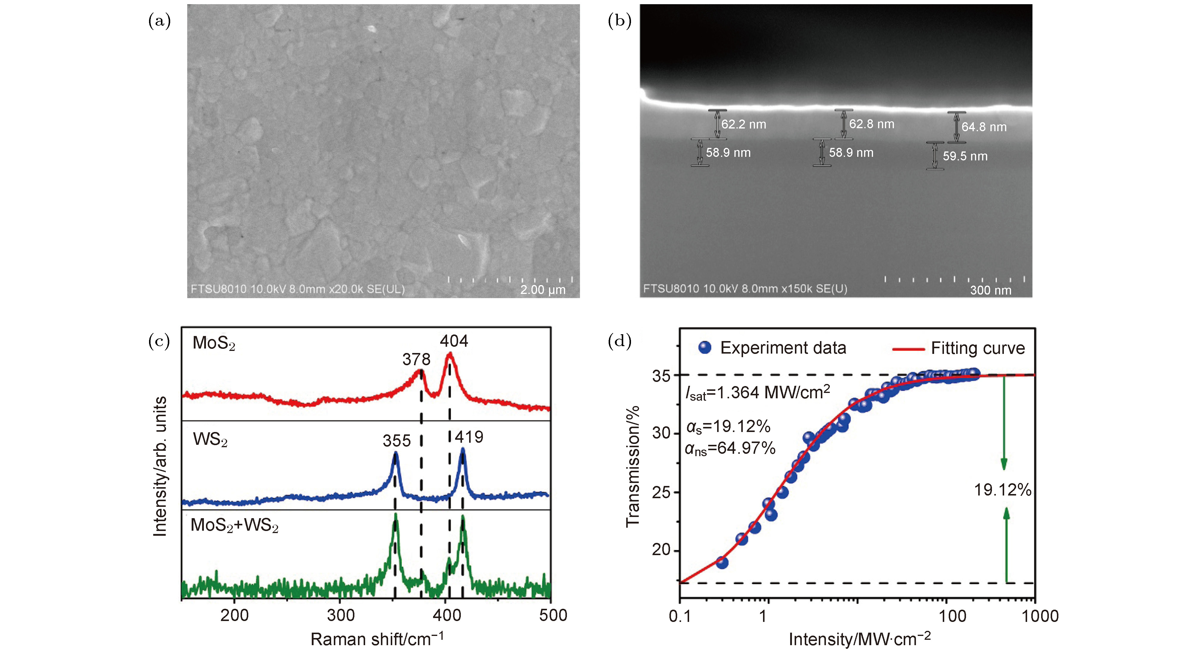
图 7 (a), (b) 磁控溅射得到的MoS2-WS2 扫描电子显微镜正面图和剖面图; (c) Raman光谱; (d) 异质结的入射光强度和透过率之间的关系图[57]
Figure 7. Scanning electron microscope images of MoS2/WS2 heterostructure from the top view (a) and side view (b); (c) Raman spectrum of MoS2, WS2 and MoS2/WS2 heterostructure; (d) transmission of MoS2/WS2 heterostructure with respect to the power intensity of incident light[57].
图 8 (a) MoS2/WS2异质结[63]; (b) MoTe2/MoS2异质结[47]; (c) MoS2/Graphene异质结[64]; (d) Bi2Te3/Graphene异质结能带及载流子迁移图[55]
Figure 8. (a) Illustration of band alignment and carrier mobility of the type-II MoS2/WS2 heterostructure[63]; (b) band alignment of semiconductor type-II MoTe2/MoS2 heterostructure[47]; (c) diagram of the charge-transfer process in a MoS2/graphene heterostructure[64]; (d) energy band diagram of Bi2Te3/graphene heterojunction, the blue dots stand for the photogenerated electrons, while red hollow dots stand for holes[55].
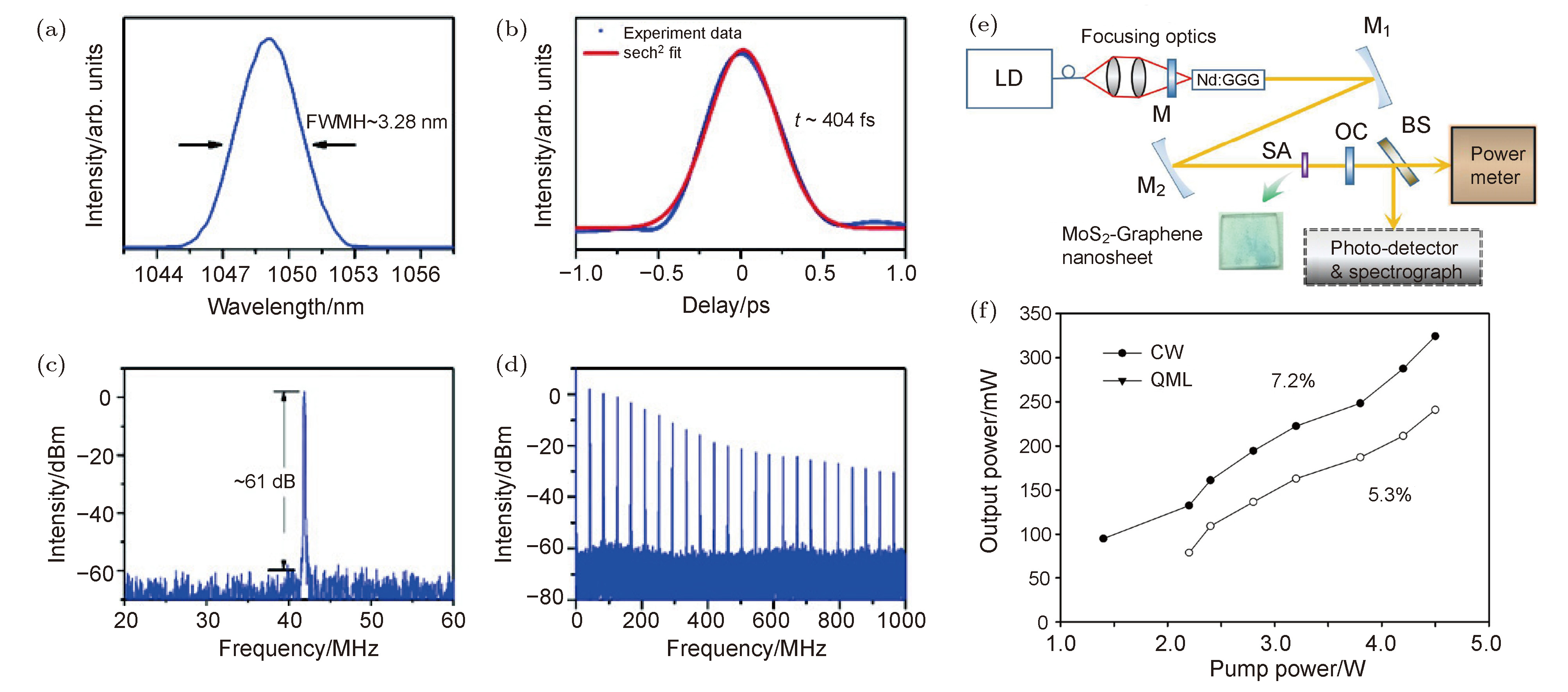
图 9 Te/BP异质结锁模激光器的输出特性 (a), (b) 测得的404 fs的自相关图和相应的频谱; (c), (d) 分别记录宽距和窄距的频谱[65]; MoS2/Graphene异质结激光器 (e)原理设置和 (f) 结构的连续波(CW)和Q开关锁模(QML)的输出功率与抽运功率关系图[34]
Figure 9. Recorded results of Te/BP heterojunction SAM-based mode-locked laser: (a), (b) measured autocorrelation trace of 404 fs and the corresponding spectrum; (c), (d) recorded frequency spectrum with a wide and a narrow span respectively[65]; (e) schematic setup of the Q-switched mode-locking (QML) laser and (f) the output power versus pump power of the continuous wave (CW) and QML operation for MoS2/Graphene heterostructure[34]

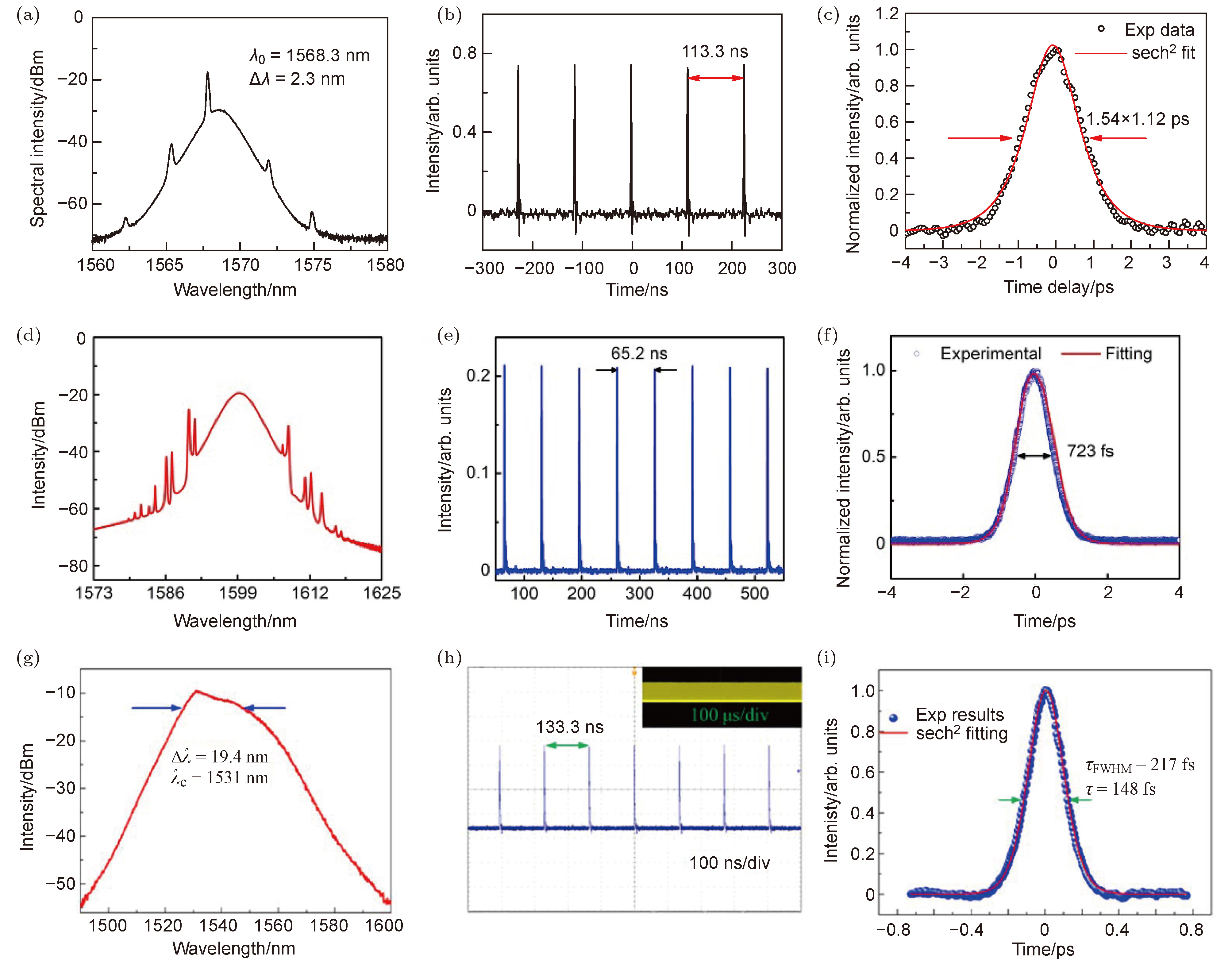
图 11 (a)−(c) Graphene/WS2异质结的锁模性能((a)光谱、(b)脉冲序列、(c)自相关曲线)[69]; (d)−(f) Graphene/Mo2C异质结的锁模性能((d)光谱、(e)脉冲序列、(f)自相关曲线)[70]; (g)−(i) Graphene/phosphorene异质结的锁模性能((g) 光谱、(h) 脉冲序列、(i) 自相关曲线)[71]
Figure 11. (a)−(c) Mode-locking performance of Graphene/WS2 heterostructure: (a) Optical spectrum; (b) pulse trains; (c) autocorrelation trace[69]. (d)−(f) Mode-locking performance of Graphene/Mo2C heterostructure: (d) Optical spectrum; (e) pulse trains; (f) autocorrelation trace[70]. (g)−(i) Mode-locking performance of Graphene/phosphorene heterostructure: (g) Optical spectrum; (h) pulse trains; (i) autocorrelation trace[71].
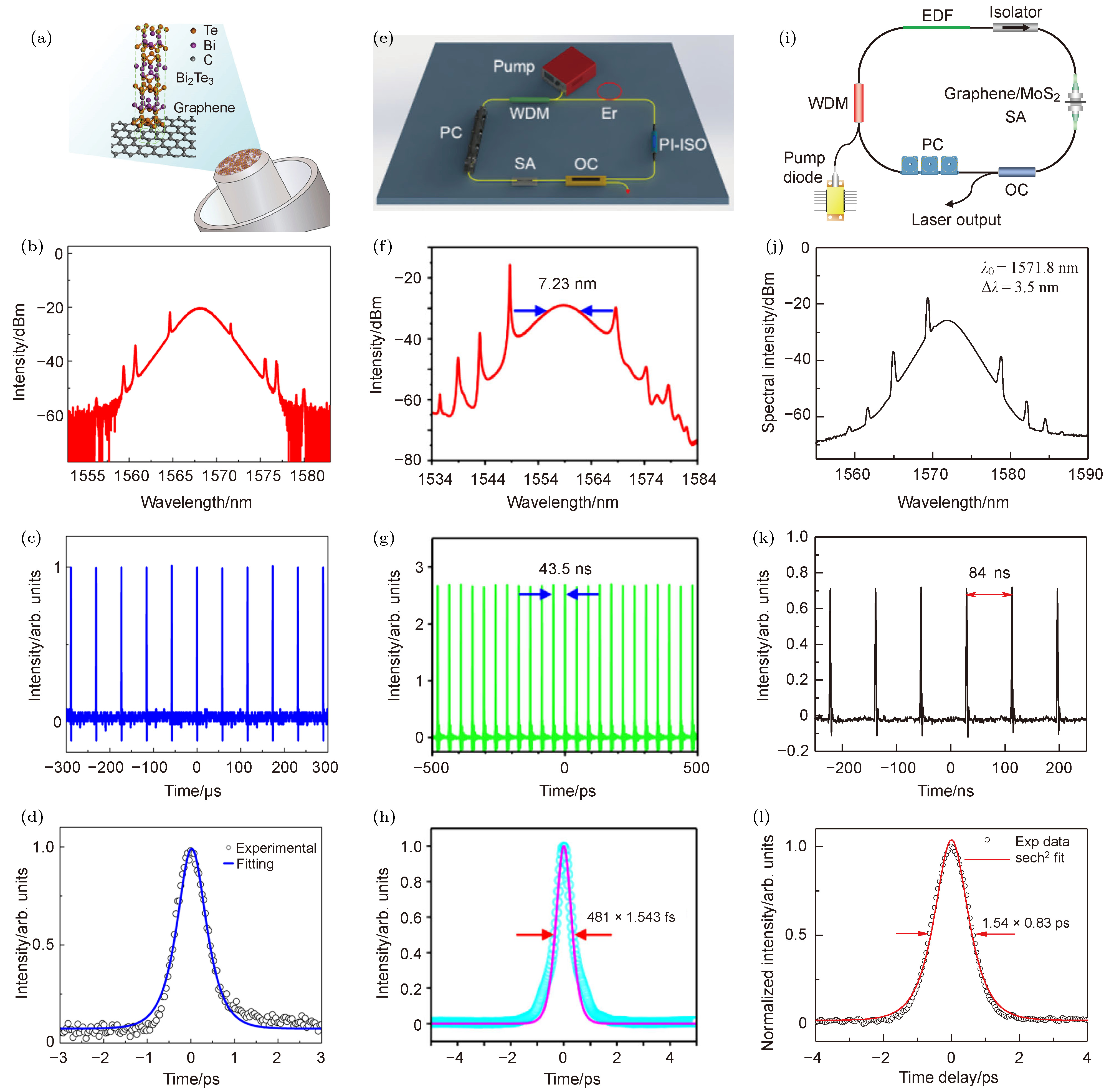
图 12 (a) Graphene/Bi2Te3异质结在光纤耦合器端面的示意图; (b)−(d) Graphene/Bi2Te3异质结的锁模特性((b) 光谱、(c) 脉冲序列、(d) 自相关曲线)[72]; (e) 掺饵光纤激光器示意图; (f)—(h) Graphene/Bi2Te3异质结的锁模特性((f) 光谱、(g) 脉冲序列、(h) 自相关曲线)[73]; (i) 掺饵光纤激光器示意图; (j)−(l) Graphene/MoS2异质结的锁模特性((j) 光谱、(k) 脉冲序列、(l) 自相关曲线)[74]
Figure 12. (a) Schematic of Graphene/Bi2Te3 heterostructure on the end-facet of fiber connector; (b)−(d) Mode-locking characteristics of Graphene/Bi2Te3 heterostructure: (b) Optical spectrum; (c) pulse trains; (d) autocorrelation trace[72]. (e) Schematic of Er-doped fiber laser. (f)−(h) Mode-locking characteristics of Bi2Te3/FeTe2 heterostructure: (f) Optical spectrum; (g) pulse trains; (h) autocorrelation trace[73]. (i) Schematic of Er-doped fiber laser. (j)−(l) Mode-locking characteristics of Graphene/MoS2 heterostructure: (j) Optical spectrum; (k) pulse trains; (l) autocorrelation trace[74].
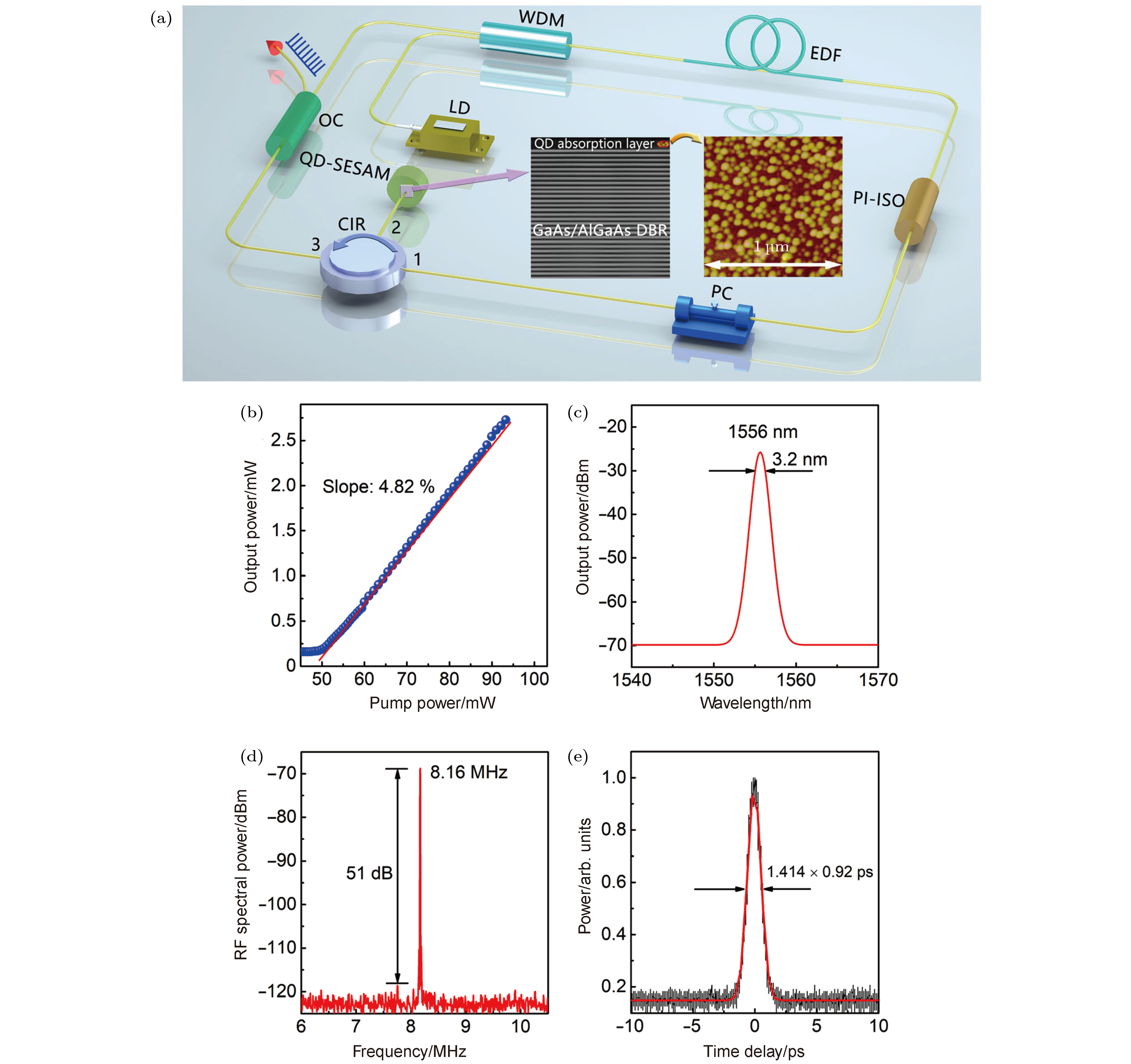
图 13 (a) InAs/GaAs QD异质结可饱和吸收镜在1550 nm锁模时所用的实验装置; 插图为量子点可饱和吸收体的截面透射电子显微镜图像和它的1 μm × 1 μm的AFM图像; (b)−(e)可饱和吸收体在1550 nm的锁模特性: (b) 输出功率与抽运功率的变化关系; (c) 输出光谱; (d) 锁模光纤激光器的RF光谱; (e) 自相关曲线[75]
Figure 13. (a) Experimental setup of mode-locked fiber laser with 1550 nm QD-SESAM; Inset: cross-sectional transmission electron microscope image of the QD-SESAM and 1 μm × 1 μm AFM image of the 1550 nm QDs. (b)−(e) Characteristics of mode-locked the developed fiber laser of InAs/GaAs QD: (b) Output power versus pump power; (c) output optical spectra; (d) RF spectrum of the mode-locked fiber laser; (e) autocorrelation trace[75].
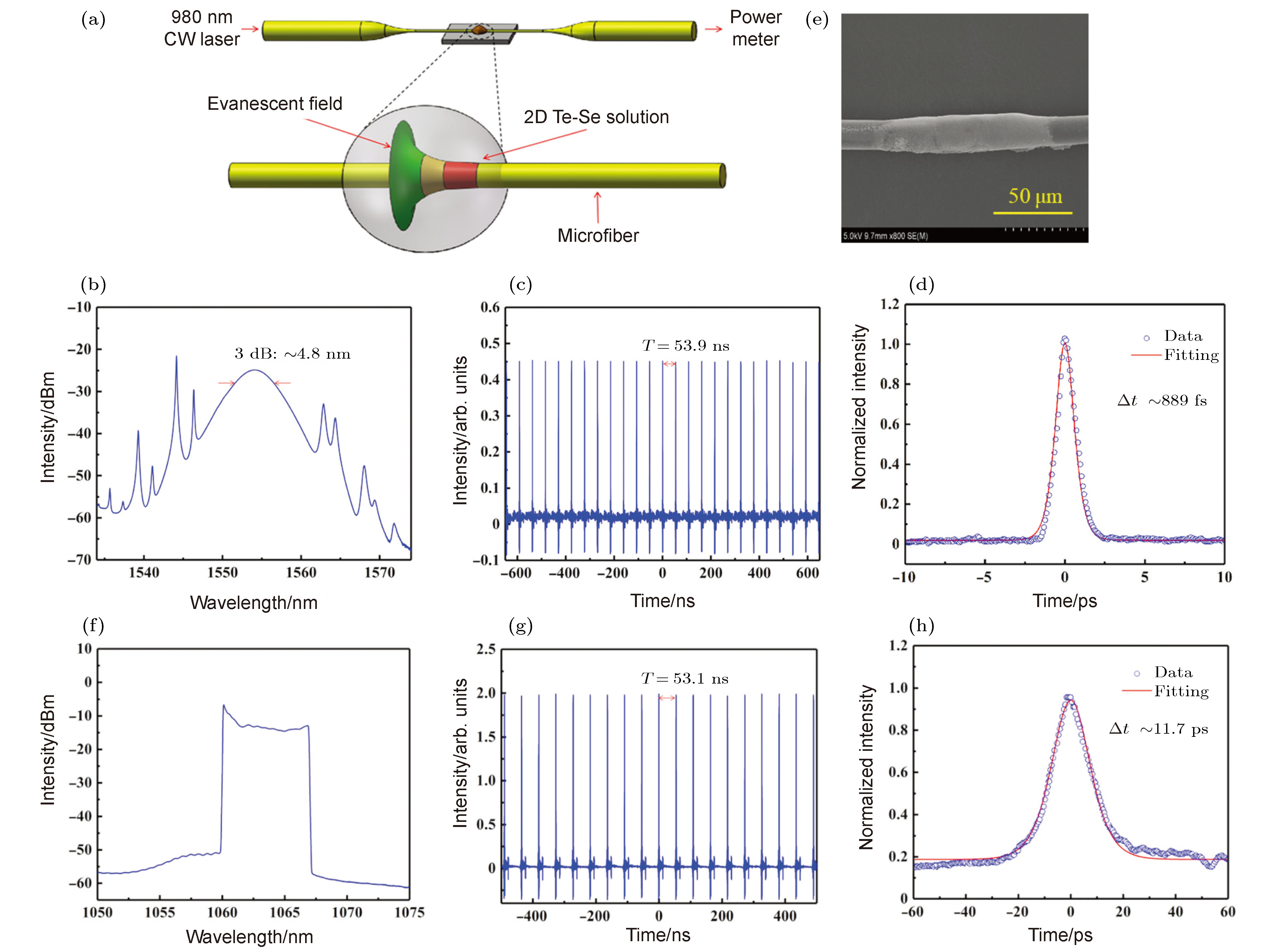
图 14 (a) 纤芯沉积样品示意图; (b)−(d)样品Te的锁模性能((b) 光谱、(c) 脉冲序列、(d) 自相关曲线); (e) 50 μm尺度下的样品显微照片; (f)—(h) 掺镱光纤激光器的自启动锁模性能((f) 光谱、(g) 脉冲序列、(h) 自相关曲线)[76]
Figure 14. (a) Schematic of deposition of the Te/Se sample on the microfiber. (b)−(d) Mode locking performance of the Te-based fiber laser: (b) Optical spectrum; (c) pulse trains; (d) autocorrelation trace. (e) Te/Se samples under microscope with 50 μm scale. (f)−(h) Self-starting mode locking performance of the Yb-doped fiber laser: (f) Optical spectrum; (g) pulse trains; (h) autocorrelation trace[76].
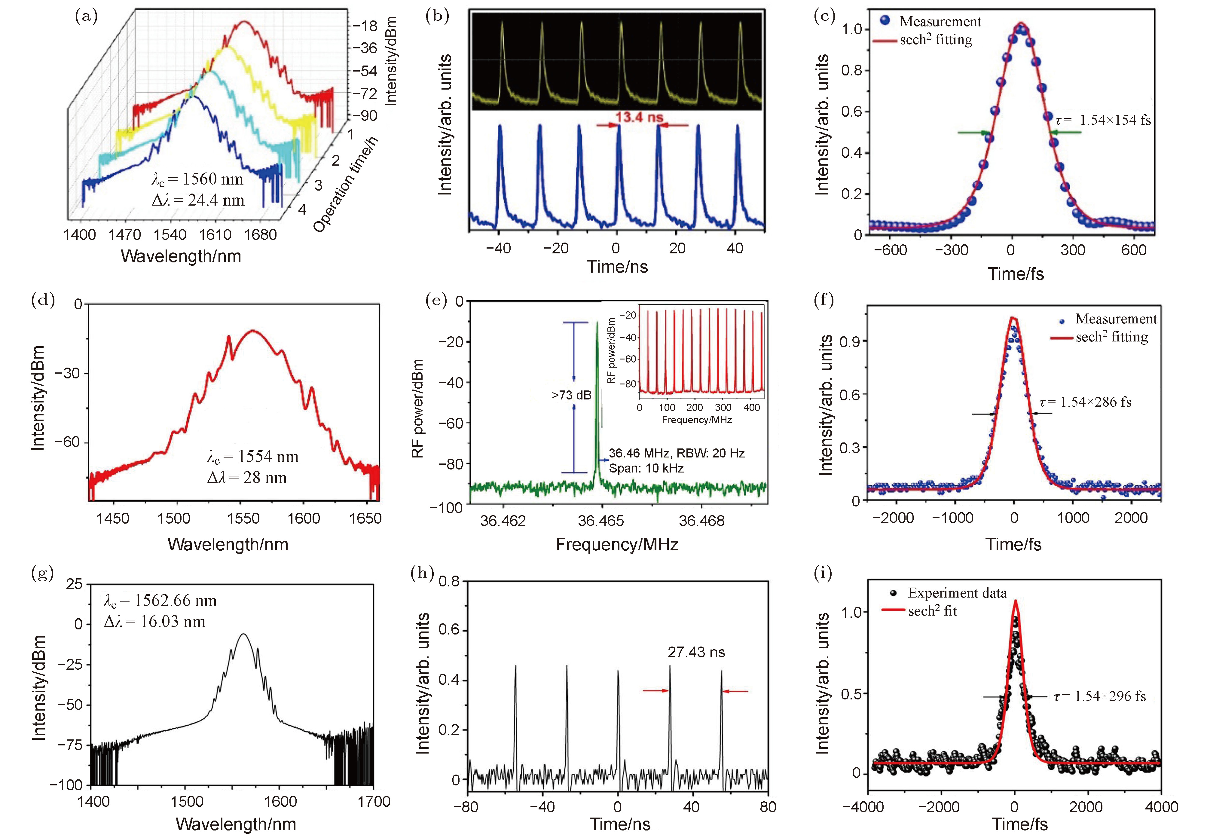
图 15 (a)—(c) MoS2/WS2异质结锁模特性((a)光谱、(b)脉冲序列、(c)自相关曲线)[57]; (d)−(f) MoS2/Sb2Te3/MoS2异质结锁模特性((d)光谱、(e)频谱、(f)自相关曲线)[77]; (g)−(i) WS2/MoS2/WS2异质结锁模特性((g)光谱、(h)频谱、(i)自相关曲线)[63]
Figure 15. (a)−(c) Mode-locking performance of MoS2/WS2 heterostructure: (a) Optical spectrum; (b) pulse trains; (c) autocorrelation trace[57]. (d)−(f) Mode-locking performance of MoS2/Sb2Te3/MoS2 heterostructure: (d) Optical spectrum; (e) pulse trains; (f) autocorrelation trace[77]. (g)−(i) Mode-locking performance of WS2/MoS2/WS2 heterostructure: (g) Optical spectrum; (h) RF spectrum; (i) autocorrelation trace[63].
表 1 基于异质结可饱和吸收体锁模激光器的性能总结
Table 1. Performance summary of mode-locked lasers based on two-dimensional heterostructure.
Material type Type of Laser Fabrication method λ/nm Pulse width Repetition rate/MHz Energy/nJ Ref. InAs/GaAs QDs FL MBE 1556.00 920.00 fs 8.16 — [75] GaN/InGaN — FIBE 408.00 1.40 ps 10.00 [78] 2D Te/BP SL LPE 1049.10 404.00 fs 42.10 6.9400 [65] Te/Se FL HM 1500.00 889.00 fs 18.50 — [76] 1000.00 11.70 ps 18.50 Graphene/MoS2 SL LPE 1061.56 306.00 ps 83.30 — [34] Graphene/MoS2 SL LPE 1063.00 92.00 fs 84.75 — [66] Graphene/MoS2 SL CVD 1037.20 236.00 fs 41.84 19.0000 [64] Graphene/MoS2 FL CVD 1571.80 830.00 fs 11.93 — [74] Graphene/MoS2 FL LPE HM 1571.80 2.20 ps 3.47 — [68] Graphene/WS2 FL CVD 1593.50 55.60 ps 3.63 — [79] Graphene/WS2 FL CVD 1568.30 1.12 ps 8.83 0.5400 [69] Graphene/WS2 FL LPE 1066.20 450.00 ps 19.68 0.1108 [80] Graphene/Mo2C FL CVD 1599.00 723.00 fs 15.33 0.7130 [70] Graphene/BP FL LPE 1529.92 820.00 fs 7.43 — [71] 1531.00 148.00 fs 7.50 Graphene/Bi2Te3 FL CVD 1565.60 1.80 ps 6.91 — [56] 1049.10 144.30 ps 3.70 Graphene/Bi2Te3 FL CVD 1568.07 837.00 fs 17.30 0.1780 [72] Graphene/Bi2Te3 FL CVD 1058.90 189.94 ps 79.13 — [81] Bi2Te3/FeTe2 FL SMD 1064.00 164.70 ps 15.02 — [73] 1550.00 481.00 fs 23.00 MoS2/graphene/WS2 FL CVD 1567.51 — 2.10 — [82] MoS2/WS2 FL MSD 1560.00 154.00 fs 74.60 — [57] WS2/MoS2/WS2 FL MSD 1562.66 296.00 fs 36.46 — [63] MoS2/Sb2Te3/MoS2 FL MSD 1554.00 286.00 fs 36.40 — [77] 注: SL, solid-state laser; FL, fiber laser; MBE, molecular beam epitaxy; FIBE, focused ion beam etching; LPE, liquid phase exfoliation; HM, hydrothermal method; CVD, chemical vapour deposition; SMD, selective metal deposition; MSD, magnetron sputtering deposition; SASR, self-assembly solvothermal route.  DownLoad: CSV
-
[1] Wu L, Huang W, Wang Y, Zhao J, Ma D, Xiang Y, Li J, Ponraj J S, Dhanabalan S C, Zhang H 2019 Adv. Funct. Mater. 29 1806346
Google Scholar
[2] Jia Y, Liao Y, Wu L, Shan Y, Dai X, Cai H, Xiang Y, Fan D 2019 Nanoscale 11 4515
Google Scholar
[3] Russo R E, Mao X, Haichen L, Gonzalez J J, Mao S S 2002 Talanta 57 425
Google Scholar
[4] Rea R, Di Matteo F M, Martino M, Pandolfi M, Saccomandi P, Rabitti C, Crescenzi A, Costamagna G 2017 Lasers Med. Sci. 32 1411
Google Scholar
[5] Kalisky Y, Kalisky O 2011 Opt. Mater. 34 457
Google Scholar
[6] Malinauskas M, Albertas Ž, Hasegawa S, Hayasaki Y, Mizeikis V, Juodkazis S 2016 Light-Sci. Appl. 5 16133
Google Scholar
[7] Woodward R, Kelleher E 2015 Appl. Sci. 5 1440
Google Scholar
[8] Okhotnikov O, Grudinin A, Pessa M 2004 New J. Phys. 6 177
Google Scholar
[9] Tang C Y, Cheng P K, Tao L, Long H, Zeng L H, Wen Q, Tsang Y H 2017 J. Light Technol. 35 4120
Google Scholar
[10] Bao Q, Zhang H, Wang Y, Ni Z, Yan Y, Shen Z X, Loh K P, Tang D Y 2009 Adv. Funct. Mater. 19 3077
Google Scholar
[11] Xu J L, Li X L, Wu Y Z, Hao X P, He J L, Yang K J 2011 Opt. Lett. 36 1948
Google Scholar
[12] 王聪, 刘杰, 张晗 2019 物理学报 68 188101
Google Scholar
Wang C, Liu J, Zhang H 2019 Acta Phys. Sin. 68 188101
Google Scholar
[13] 张倩, 金鑫, 张梦, 郑铮 2020 物理学报 69 188101
Google Scholar
Zhang Q, Jin X X, Zhang M, Zheng Z 2020 Acta Phys. Sin. 69 188101
Google Scholar
[14] Long H, Tang C Y, Cheng P K, Wang X Y, Qarony W, Tsang Y H 2019 J. Lightwave Technol. 37 1174
Google Scholar
[15] Long H, Shi Y, Wen Q, Tsang Y H 2019 J. Mater. Chem. C 7 5937
Google Scholar
[16] He J, Tao L, Zhang H, Zhou B, Li J 2019 Nanoscale 11 2577
Google Scholar
[17] Tao L, Huang X, He J, Lou Y, Zeng L, Li Y, Long H, Li J, Zhang L, Tsang Y H 2018 Photonics Res. 6 750
Google Scholar
[18] Yu H, Zheng X, Yin K, Cheng X, Jiang T 2015 Appl. Opt. 54 10290
Google Scholar
[19] Luo Z, Huang Y, Zhong M, Li Y, Wu J, Xu B, Xu H, Cai Z, Peng J, Weng J 2014 J. Lightwave Technol. 32 4077
[20] Yan P, Liu A, Chen Y, Wang J, Ruan S, Chen H, Ding J 2015 Sci. Rep. 5 12587
Google Scholar
[21] Luo Z C, Liu M, Guo Z N, Jiang X F, Luo A P, Zhao C J, Yu X F, Xu W C, Zhang H 2015 Opt. Express 23 20030
Google Scholar
[22] Ming N, Tao S, Yang W, Chen Q, Sun R, Wang Ch, Wang S, Man B, Zhang H 2018 Opt. Express 26 9017
Google Scholar
[23] Lee Y W, Chen C M, Huang C W, Chen S K, Jiang J R 2016 Opt. Express 24 10675
Google Scholar
[24] Sun Z, Hasan T, Torrisi F, Popa D, Privitera G, Wang F, Bonaccorso F, Basko D M, Ferrari A C 2010 ACS Nano 4 803
Google Scholar
[25] Chen Y, Jiang G, Chen S, Guo Z, Yu X, Zhao C, Zhang H, Bao Q, Wen S, Tang D, Fan D 2015 Opt. Express 23 12823
Google Scholar
[26] Wang Y, Lee P, Zhang B, Sang Y, He J 2017 Nanoscale 9 19100
Google Scholar
[27] Jiang X, Liu S, Liang W, Luo S, He Z, Ge Y, Wang H, Cao R, Zhang F, Wen Q, Li J, Bao Q 2017 Laser Photonics Rev. 12 1700229
Google Scholar
[28] Wang Y, Huang G, Mu H, Lin S, Chen J, Xiao S, Bao Q, He J 2015 Appl. Phys. Lett. 107 091905
Google Scholar
[29] Geim A K, Grigorieva I V 2013 Nature 499 419
Google Scholar
[30] Liu L, Chu H, Zhang X, Pan H, Zhao S, Li D 2019 Nanoscale Res. Lett. 14 112
Google Scholar
[31] Zhang H, Zhang F, Li X, Chen L, Wang J, Wang L 2017 Opt. Mater. 70 153
Google Scholar
[32] Li Z, Cheng C, Dong N, Romero C, Lu Q, Wang J, Rodríguez Vázquez de Aldana J, Tan Y, Chen F 2017 Photonics Res. 5 406
Google Scholar
[33] You Z, Sun Y, Sun D, Zhu Z, Wang Y, Li J, Tu C, Xu J 2017 Opt. Lett. 42 871
Google Scholar
[34] Wen Y, Zhao X S, Zhang W 2018 Optik 170 90
Google Scholar
[35] Zhao G, Lv X, Xie Z, Xu J 2017 Conference on Lasers and Electro-Optics Pacific Rim (CLEO-PR) Singapore, July 31−Aug 4, 2017 p1
[36] Stankovich S, Dikin D A, Dommett G H B, Kohlhaas K M, Zimney E J, Stach E A, Piner R D, Nguyen S T, Ruoff R S 2006 Nature 442 282
Google Scholar
[37] He J, Wang C, Zhou B, Zhao Y, Tao L, Zhang H 2020 Mater. Horiz.
Google Scholar
[38] Novoselov K S, Geim A K, Morozov S V, Jiang D, Zhang Y, Dubonos S V, Grigorieva I V, Firsov A A 2004 Science 306 666
Google Scholar
[39] Wu J, Li H, Yin Z, Li H, Liu J, Cao X, Zhang Q, Zhang H 2013 Small 9 3314
Google Scholar
[40] Pezeshki A, Shokouh S H H, Nazari T, Oh K, Im S 2016 Adv. Mater. 28 3216
Google Scholar
[41] Wang W, Chen S J, Basquiroto de Souza F, Wu B, Duan W H 2018 Nanoscale 10 1004
Google Scholar
[42] Lu L, Liang Z, Wu L, Chen Y X, Song Y, Dhanabalan S C, Ponraj J S, Dong B, Xiang Y, Xing F, Fan D, Zhang H 2018 Laser Photonics Rev. 12 1700221
Google Scholar
[43] Kim J, Kwon S, Cho D H, Kang B, Kwon H, Kim Y, Park S O, Jung G Y, Shin E, Kim W G, Lee H, Ryu G H, Choi M, Kim T H, Oh J, Park S, Kwak S K, Yoon S W, Byun D, Lee Z, Lee C 2015 Nat. Commun. 6 8294
Google Scholar
[44] Tao L, Long H, Zhou B, Yu S F, Lau S P, Chai Y, Fung K H, Tsang Y H, Yao J, Xu D 2014 Nanoscale 6 9713
Google Scholar
[45] Shi Y, Long H, Liu S, Tsang Y H, Wen Q 2018 J. Mater. Chem. C 6 12638
Google Scholar
[46] Lu C, Quan C, Si K, Xu X, He C, Zhao Q, Zhan Y, Xu X 2019 Appl. Surf. Sci. 479 1161
Google Scholar
[47] Quan C, Lu C, He C, Xu X, Huang Y, Zhao Q, Xu X 2019 Adv. Mater. Interfaces 6 1801733
Google Scholar
[48] Lee Y H, Zhang X Q, Zhang W, Chang M T, Lin C Te, Chang K Di, Yu Y C, Wang J T W, Chang C S, Li L J, Lin T W 2012 Adv. Mater. 24 2320
Google Scholar
[49] Reina A, Jia X, Ho J, Nezich D, Son H, Bulovic V, Dresselhaus M, Jing K, Kong J 2008 Nano Lett. 9 30
Google Scholar
[50] Schmidt H, Wang S, Chu L, Toh M, Kumar R, Zhao W, Neto A H C, Martin J, Adam S, Oezyilmaz B, Eda G 2014 Nano Lett. 14 1909
Google Scholar
[51] Zhan Y, Liu Z, Najmaei S, Ajayan P M, Lou J 2012 Small 8 966
Google Scholar
[52] Cong C, Shang J, Wu X, Cao B, Peimyoo N, Qiu C, Litao S, Yu T 2014 Adv. Opt. Mater. 2 12512
Google Scholar
[53] Hong X, Kim J, Shi S-F, Zhang Y, Jin C, Sun Y, Tongay S, Wu J, Zhang Y, Wang F 2014 Nat. Nanotechnol. 9 682
Google Scholar
[54] Chen H, Wen X, Zhang J, Wu T, Gong Y, Zhang X, Yuan J, Yi C, Lou J, Ajayan P M, Zhuang W, Zhang G, Zheng J 2016 Nat. Commun. 7 1
Google Scholar
[55] Qiao H, Yuan J, Xu Z, Chen C, Lin S, Wang Y, Song J, Liu Y, Khan Q, Hoh H Y, Pan C X, Li S, Bao Q 2015 ACS Nano 9 1886
Google Scholar
[56] Wang Z, Mu H, Yuan J, Zhao C, Bao Q, Zhang H 2017 IEEE J. Sel. Top. Quantum Electron. 23 8800105
Google Scholar
[57] Liu W J, Liu M L, Liu B, Quhe R G, Lei M, Fang S B, Teng H, Wei Z Y 2019 Opt. Express 27 6689
Google Scholar
[58] Lee J, Shin J H, Lee G H, Lee C H 2016 Nanomaterials 6 193
Google Scholar
[59] Velický M, Toth P S 2017 Appl. Mater. Today 8 68
Google Scholar
[60] Liu B, Long M, Cai M Q, Yang J 2018 J. Phys. Chem. Lett. 9 4822
Google Scholar
[61] Niu T, Li A 2015 Prog. Surf. Sci. 90 21
Google Scholar
[62] Ma S, Zeng L, Tao L, Tang C Y, Yuan H, Long H, Cheng P K, Chai Y, Chen C, Fung K H, Zhang X, Lau S P, Tsang Y H 2017 Sci. Rep. 7 3125
Google Scholar
[63] Chen H, Yin J, Yang J, Zhang X, Liu M, Jiang Z, Wang J, Sun Z, Guo T, Liu W, Yan P 2017 Opt. Lett. 42 4279
Google Scholar
[64] Sun X, Zhang B, Li Y, Luo X, Li G, Chen Y, Zhang C, He J 2018 ACS Nano 12 11376
Google Scholar
[65] Yan B, Li G, Shi B, Liu J, Nie H, Yang K, Zhang B, He J 2020 Nanophotonics 9 2593
Google Scholar
[66] 祎然 2019 博士学位论文 (济南: 山东大学)
Wang Y R 2019 Ph. D. Dissertation (Jinan: ShanDong University) (in Chinese)
[67] Zhao G, Hou J, Wu Y, He J, Hao X 2015 Adv. Opt. Mater. 3 937
Google Scholar
[68] Jiang Y, Miao L, Jiang G, Chen Y, Qi X, Jiang X 2015 Sci. Rep. 5 16372
Google Scholar
[69] Du W, Li H, Liu C, Shen S, Liu Y, Lan C, Li C 2017 Proc. SPIE 10457, AOPC 2017: Laser Components, Systems, and Applications Beijing, China, October 24, 2017 104571 M
[70] Mu H, Tuo M, Xu C, Bao X, Xiao S, Sun T, Li L, Zhao L, Li S, Ren W, Bao Q 2019 Opt. Mater. Express 9 3268
Google Scholar
[71] Liu S, Li Z, Ge Y, Wang H, Yue R, Jiang X, Li J, Wen Q, Zhang H 2017 Photonics Res. 5 662
Google Scholar
[72] Mu H, Wang Z, Yuan J, Xiao S, Chen C, Chen Y, Chen Y, Song J, Wang Y, Xue Y, Zhang H, Bao Q 2015 ACS Photonics 2 832
Google Scholar
[73] Zhang L, Liu J, Li J, Wang Z, Wang Y, Ge Y, Dong W, Xu N, He T, Zhang H, Zhang W 2020 Laser Photonics Rev. 14 1900409
Google Scholar
[74] Liu C, Li H, Deng G, Lan C, Li C, Liu Y 2016 2016 Asia Communications and Photonics Conference (ACP) Wuhan, China, Novermber 2−5, 2016 p1
[75] Jiang C, Ning J, Li X, Wang X, Zhang Z 2019 Nanoscale Res. Lett. 14 15252
[76] Song Y, You K, Zhao J, Huang D, Chen Y, Xing C, Zhang H 2020 Nanoscale 12 15252
Google Scholar
[77] Liu W, Zhu Y N, Liu M, Wen B, Fang S, Teng H, Lei M, Liu L M, Wei Z 2018 Photonics Res. 6 220
Google Scholar
[78] Olle V F, Vasil’v P P, Wonfor A, Penty R V, White I H 2012 Opt. Express 20 7035
Google Scholar
[79] Du W, Li H, Lan C, Li C, Li J, Wang Z, Liu Y 2020 Opt. Express 28 11514
Google Scholar
[80] Ma X, Lu B, Qi X, Lu C, Li D, Wen Z, Xu X, Bai J 2019 Appl. Phys. Express 12 112006
Google Scholar
[81] Wang Z, Mu H, Zhao C, Bao Q, Zhang H 2016 Opt. Eng. 55 081314
Google Scholar
[82] Chen H, Li I L, Zhang M, Wang J, Yan P 2017 Opto-Electronics Commun. Conf. OECC 2017 Photonics Glob. Conf. PGC Singapore, July 31−Aug 4, 2017 p1

 DownLoad:
Catalog
Metrics
- Abstract views: 13095
- PDF Downloads: 418
- Cited By: 0
