


-
Two-dimensional (2D) material has atomic smooth surface, nano-scale thickness and ultra-high specific surface area, which is an important platform for studying the interface interaction between metal nanoparticles (NPs) and 2D materials, and also for observing the surface atomic migration, structural evolution and aggregation of metal NPs in real time and in situ. By rationally designing and constructing the interfaces of metal NPs and 2D materials, the characterization of the interface structure on an atomic scale is very important in revealing the structure-property relationship. It is expected that the investigation is helpful in understanding the mechanism of interaction between metal and 2D materials and optimizing the performance of the devices based on metal-2D material heterojunctions. In this review, the recent progress of interface modulation and physical properties of the heterostructure of metal NPs and 2D materials are summarized. The nucleation, growth, structural evolution and characterization of metal NPs on the surface of 2D materials are reviewed. The effects of metal NPs on the crystal structure, electronic state and energy band of 2D materials are analyzed. The possible interfacial strain and interfacial reaction are also included. Because of the modulation of electrical and optical properties of 2D materials, the performance of metal NPs-2D material based field effect transistor devices and optoelectronic devices are improved. This review is helpful in clarifying the physical mechanism of microstructure affecting the properties of metal NPs-2D material heterostructures on an atomic scale, and also in developing the metal-2D material heterostructures and their applications in the fields of electronic devices, photoelectric devices, energy devices, etc. -
Keywords:
- two-dimensional materials /
- plasmon resonance /
- interface structure /
- transmission electron microscopy
[1] Geim A K, Novoselov K S 2007 Nat. Mater. 6 183
 Google Scholar
[2] Chen J H, Jang C, Xiao S, Ishigami M, Fuhrer M S 2008 Nat. Nanotechnol. 3 206
Google Scholar
[3] Balandin A A, Ghosh S, Bao W, Calizo I, Teweldebrhan D, Miao F, Lau C N 2008 Nano Lett. 8 902
Google Scholar
[4] Lee C, Wei X, Kysar J W, Hone J 2008 Science 321 385
Google Scholar
[5] Panchokarla L S, Subrahmanyam K S, Saha S K, Govindaraj A, Krishnamurthy H R, Waghmare U V, Rao C N R 2009 Adv. Mater. 21 4726
[6] Wei D, Liu Y, Wang Y, Zhang H, Huang L, Yu G 2009 Nano Lett. 9 1752
Google Scholar
[7] Latorre-Sanchez M, Primo A, Garcia H 2013 Angew. Chem. Int. Edit. 52 11813
Google Scholar
[8] Jiao L, Zhang L, Wang X, Diankov G, Dai H 2009 Nature 458 877
Google Scholar
[9] Jiao L, Wang X, Diankov G, Wang H, Dai H 2010 Nat. Nanotechnol. 5 321
Google Scholar
[10] Radisavljevic B, Radenovic A, Brivio J, Giacometti V, Kis A 2011 Nat. Nanotechnol. 6 147
Google Scholar
[11] Wang Q H, Kalantar-Zadeh K, Kis A, Coleman J N, Strano M S 2012 Nat. Nanotechnol. 7 699
Google Scholar
[12] Mak K F, Shan J 2016 Nat. Photonics 10 216
Google Scholar
[13] Lü R, Terrones H, Elias A L, Perea-Lopez N, Gutierrez H R, Cruz-Silva E, Rajukumar L P, Dresselhaus M S, Terrones M 2015 Nano Today 10 559
Google Scholar
[14] Tan C L, Cao X H, Wu X J, He Q Y, Yang J, Zhang X, Chen J Z, Zhao W, Han S K, Nam G H, Sindoro M, Zhang H 2017 Chem. Rev. 117 6225
Google Scholar
[15] Zhou L, Xia T, Cao T, Wang L, Chen Y, Li S, Wang R, Guo H 2020 J. Alloys Compd. 818 152909
Google Scholar
[16] Najmaei S, Mlayah A, Arbouet A, Girard C, Leotin J, Lou J 2014 ACS Nano 8 12682
Google Scholar
[17] Xiu X W, Zhang W C, Hou S T, Li Z, Lei F C, Xu S C, Li C H, Man B Y, Yu J, Zhang C 2021 Chin. Phys. B 30 088801
Google Scholar
[18] Zan R, Bangert U, Ramasse Q, Novoselov K S 2011 Small 7 2868
Google Scholar
[19] Zan R, Bangert U, Ramasse Q, Novoselov K S 2012 J. Phys. Chem. Lett. 3 953
Google Scholar
[20] Chen Q, He K, Robertson A W, Kirkland A I, Warner J H 2016 ACS Nano 10 10418
Google Scholar
[21] Zhou H, Yu F, Guo C F, Wang Z, Lan Y, Wang G, Fang Z, Liu Y, Chen S, Sun L F, Ren Z 2015 Nanoscale 7 9153
Google Scholar
[22] Jin Z, Nackashi D, Lu W, Kittrell C, Tour J M 2010 Chem. Mater. 22 5695
Google Scholar
[23] Wang S, Sawada H, Chen Q, Han G G D, Allen C, Kirkland A I, Warner J H 2017 ACS Nano 11 9057
Google Scholar
[24] Wang S, Sawada H, Han X, Zhou S, Li S, Guo Z X, Kirkland A I, Warner J H 2018 ACS Nano 12 5626
Google Scholar
[25] Zuo P, Jiang L, Li X, Li B, Xu Y, Shi X, Ran P, Ma T, Li D, Qu L, Lu Y, Grigoropoulos C P 2017 ACS Appl. Mater. Interfaces 9 7447
Google Scholar
[26] Lei Y T, Li D W, Zhang T C, Huang X, Liu L, Lu Y F 2017 J. Mater. Chem. C 5 8883
Google Scholar
[27] Liu X W, Wang D S, Li Y D 2012 Nano Today 7 448
Google Scholar
[28] Huang X, Li S, Wu S, Huang Y, Boey F, Gan C L, Zhang H 2012 Adv. Mater. 24 979
Google Scholar
[29] Kidd T E, Weber J, Holzapfel R, Doore K, Stollenwerk A J 2018 Appl. Phys. Lett. 113 191603
Google Scholar
[30] Muszynski R, Seger B, Kamat P V 2008 J. Phys. Chem. C 112 5263
Google Scholar
[31] Kamat P V 2010 J. Phys. Chem. Lett. 1 520
Google Scholar
[32] Li Y, Fan X, Qi J, Ji J, Wang S, Zhang G, Zhang F 2010 Nano Res. 3 429
Google Scholar
[33] Yuk J M, Jeong M, Kim S Y, Seo H K, Kim J, Lee J Y 2013 Chem. Commun. 49 11479
Google Scholar
[34] Sun Y, Zhao H, Zhou D, Zhu Y, Ye H, Moe Y A, Wang R 2019 Nano Res. 12 947
Google Scholar
[35] Lu X, Luo X, Zhang J, Quek S Y, Xiong Q 2016 Nano Res. 9 3559
Google Scholar
[36] Wu J B, Lin M L, Cong X, Liu H N, Tan P H 2018 Chem. Soc. Rev. 47 1822
Google Scholar
[37] Lee C, Yan H, Brus L E, Heinz T F, Hone J, Ryu S 2010 ACS Nano 4 2695
Google Scholar
[38] Liu H T, Ryu S M, Chen Z Y, Steigerwald M L, Nuckolls C, Brus L E 2009 J. Am. Chem. Soc. 131 17099
Google Scholar
[39] Martins F E H, Moutinho M V O, Stavale F, Lucchese M M, Capaz R B, Achete C A, Jorio A 2010 Phys. Rev. B 82 125429
Google Scholar
[40] Lui C H, Malard L M, Kim S, Lantz G, Laverge F E, Saito R, Heinz T F 2012 Nano Lett. 12 5539
Google Scholar
[41] Wu J B, Zhang X, Ijaes M, Han W P, Qiao X F, Li X L, Jiang D S, Ferrari A C, Tan P H 2014 Nat. Commun. 5 5309
Google Scholar
[42] Zhang X, Han W P, Qiao X F, Tan Q H, Wang Y F, Zhang J, Tan P H 2016 Carbon 99 118
Google Scholar
[43] Zhang X, Han W P, Wu J B, Milana S, Lu Y, Li Q Q, Ferrari A C, Tan P H 2013 Phys. Rev. B 87 115413
Google Scholar
[44] Zhao H, Wu J B, Zhong H X, Guo Q S, Wang X M, Xia F N, Yang L, Tan P H, Wang H 2015 Nano Res. 8 3651
Google Scholar
[45] Liu K, Zhang L, Cao T, Jin C, Qiu D, Zhou Q, Zettl A, Yang P, Louie S G, Wang F 2014 Nat. Commun. 5 4966
Google Scholar
[46] Wang P, Zhang D, Zhang L, Fang Y 2013 Chem. Phys. Lett. 556 146
Google Scholar
[47] Qiu C, Zhou H, Cao B, Sun L, Yu T 2013 Carbon 59 487
Google Scholar
[48] Gong C, Huang C, Miller J, Cheng L, Hao Y, Cobden D, Kim J, Ruoff R S, Wallace R M, Cho K, Xu X, Chabal Y J 2013 ACS Nano 7 11350
Google Scholar
[49] Sun Y, Moe Y A, Xu Y, Sun Y, Wang X, Li F, Liu K, Wang R 2019 Nanoscale 11 22432
Google Scholar
[50] Sun Y H, Liu K, Hong X P, Chen M, Kim J, Shi S F, Wu J Q, Zettl A, Wang F 2014 Nano Lett. 14 5329
Google Scholar
[51] Moe Y A, Sun Y H, Ye H Y, Liu K, Wang R 2018 ACS Appl. Mater. Interfaces 10 40246
Google Scholar
[52] Boukhvalov D W, Katsnelson M I 2009 Appl. Phys. Lett. 95 023109
[53] Campos L C, Manfrinato V R, Sanchez-Yamagishi J D, Kong J, Jarillo-Herrero P 2009 Nano Lett. 9 2600
Google Scholar
[54] Sreeprasad T S, Phong N, Kim N, Berry V 2013 Nano Lett. 13 4434
Google Scholar
[55] Chen C H, Wu C L, Pu J, Chiu M H, Kumar P, Takenobu T, Li L J 2014 2D Mater. 1 034001
[56] Shi Y, Huang J K, Jin L, Hsu Y T, Yu S F, Li L J, Yang H Y 2013 Sci. Rep. 3 1839
Google Scholar
[57] Li W W, Geng X M, Guo Y F, Rong J Z, Gong Y P, Wu L Q, Zhang X M, Li P, Xu J B, Cheng G S, Sun M T, Liu L W 2011 ACS Nano 5 6955
Google Scholar
[58] He Q, Zeng Z, Yin Z, Li H, Wu S, Huang X, Zhang H 2012 Small 8 2994
Google Scholar
[59] Chen K, Lu G, Chang J, Mao S, Yu K, Cui S, Chen J 2012 Anal. Chem. 84 4057
Google Scholar
[60] Xu W G, Mao N N, Zhang J 2013 Small 9 1206
Google Scholar
[61] Jing X X, Li D Q, Zhang Y, Hou X Y, Jiang J, Fan X C, Wang M C, Feng S P, Yu Y F, Lu J P, Hu Z L, Ni Z H 2021 Chin. Phys. Lett. 38 074203
Google Scholar
[62] Li J H, Zhang S N, Zhai Y J, Ma J G, Fang W H, Zhang Y 2019 Acta Phys. Sin. 68 134203
Google Scholar
[63] Huang J, Zhang L, Chen B, Ji N, Chen F, Zhang Y, Zhang Z 2010 Nanoscale 2 2733
Google Scholar
[64] Hou H, Wang P, Zhang J, Li C, Jin Y 2015 ACS Appl. Mater. Interfaces 7 18038
Google Scholar
[65] Liu M, Chen W 2013 Biosens. Bioelectron. 46 68
Google Scholar
[66] Gupta S, Banaszak A, Smith T, Dimakis N 2018 J. Raman Spectrosc. 49 438
Google Scholar
[67] Singha S S, Nandi D, Singha A 2015 RSC Adv. 5 24188
Google Scholar
[68] Lee B, Park J, Han G H, Ee H S, Naylor C H, Liu W, Johnson A T C, Agarwal R 2015 Nano Lett. 15 3646
Google Scholar
[69] Mak K F, Lee C, Hone J, Shan J, Heinz T F 2010 Phys. Rev. Lett. 105 136805
Google Scholar
[70] Lee K C J, Chen Y H, Lin H Y, Cheng C C, Chen P Y, Wu T Y, Shih M H, Wei K H, Li L J, Chang C W 2015 Sci. Rep. 5 16374
Google Scholar
[71] Butun S, Tongay S, Aydin K 2015 Nano Lett. 15 2700
Google Scholar
[72] Sobhani A, Lauchner A, Najmaei S, Ayala-Orozco C, Wen F, Lou J, Halas N J 2014 Appl. Phys. Lett. 104 031112
Google Scholar
[73] Li J, Nie C, Sun F, Tang L, Zhang Z, Zhang J, Zhao Y, Shen J, Feng S, Shi H, Wei X 2020 ACS Appl. Mater. Interfaces 12 8429
Google Scholar
[74] Gao W, Lee Y H, Jiang R, Wang J, Liu T, Ling X Y 2016 Adv. Mater. 28 701
Google Scholar
[75] Zhang H Z, Xu C Y, Nan H Y, Xiao S Q, Gu X F 2020 Acta Phys. Sin. 69 246101
Google Scholar
[76] Chi Z H, Zhao X M, Zhang H, Goncharov A F, Lobanov S S, Kagayama T, Sakata M, Chen X J 2014 Phys. Rev. Lett. 113 036802
Google Scholar
[77] Nayak A P, Bhattacharyya S, Zhu J, Liu J, Wu X, Pandey T, Jin C, Singh A K, Akinwande D, Lin J F 2014 Nat. Commun. 5 3731
Google Scholar
[78] Liu B, Han Y H, Gao C X, Ma Y Z, Peng G, Wu B J, Liu C L, Wang Y, Hu T J, Cui X Y, Ren W B, Li Y, Su N N, Liu H W, Zou G T 2010 J. Phys. Chem. C 114 14251
Google Scholar
[79] Lin Y C, Dumcencon D O, Huang Y S, Suenaga K 2014 Nat. Nanotechnol. 9 391
Google Scholar
[80] Loh T A J, Chua D H C 2015 J. Phys. Chem. C 119 27496
Google Scholar
[81] Py M A H, Haering R R 1983 Can. J. Phys. 61 76
Google Scholar
[82] Wang L, Xu Z, Wang W, Bai X D 2014 J. Am. Chem. Soc. 136 6693
Google Scholar
[83] Wang X F, Shen X, Wang Z X, Yu R C, Chen L Q 2014 ACS Nano 8 11394
Google Scholar
[84] Kang Y, Najmaei S, Liu Z, Bao Y, Wang Y, Zhu X, Halas N J, Nordlander P, Ajayan P M, Lou J, Fang Z Y 2014 Adv. Mater. 26 6467
Google Scholar
[85] Gong C, Zhang H J, Wang W H, Colombo L, Wallace R M, Cho K J 2013 Appl. Phys. Lett. 103 053513
Google Scholar
[86] Kang Y, Gong Y, Hu Z, Li Z, Qiu Z, Zhu X, Ajayan P M, Fang Z 2015 Nanoscale 7 4482
Google Scholar
[87] Wei S, Cui X Q, Xu Y, Shang B, Zhang Q, Gu L, Fan X, Zheng L, Hou C, Huang H, Wen S, Zheng W T 2019 ACS Energy Lett. 4 368
Google Scholar
[88] Shang B, Cui X Q, Jiao L, Qi K, Wang Y W, Fan J C, Yue Y Y, Wang H Y, Bao Q L, Fan X F, Wei S T, Song W, Cheng Z L, Guo S J, Zheng W T 2019 Nano Lett. 19 2758
Google Scholar
[89] Qi K, Cui X Q, Gu L, Yu S, Fan X, Luo M, Xu S, Li N, Zheng L, Zhang Q, Ma J, Gong Y, Lü F, Wang K, Huang H, Zhang W, Guo S, Zheng W T, Liu P 2019 Nat. Commun. 10 5231
Google Scholar
[90] Miao J, Hu W, Jing Y, Luo W, Liao L, Pan A, Wu S, Cheng J, Chen X, Lu W 2015 Small 11 2392
Google Scholar
[91] Lan H Y, Hsieh Y H, Chiao Z Y, Jariwala D, Shih M H, Yen T J, Hess O, Lu Y J 2021 Nano Lett. 21 3083
Google Scholar
[92] Chen W, Liang R, Liu Y, Zhang S, Cheng W, Zhao L, Xu J 2019 Appl. Phys. Lett 115 142102
Google Scholar
[93] Han X, Xing J, Xu H, Huang Y, Li D, Lu J, Li P, Wu Y 2020 Nanotechnology 31 215201
Google Scholar
[94] Sriram P, Wen Y P, Manikandan A, Hsu K C, Tang S Y, Hsu B W, Chen Y Z, Lin H W, Jeng H T, Chueh Y L, Yen T J 2020 Chem. Mater. 32 2242
Google Scholar
[95] Fang Z Y, Liu Z, Wang Y, Ajayan P M, Nordlander P, Halas N J 2012 Nano Lett. 12 3808
Google Scholar
[96] Kumar R, Sharma A, Kaur M, Husale S 2017 Adv. Opt. Mater 5 1700009
Google Scholar
-
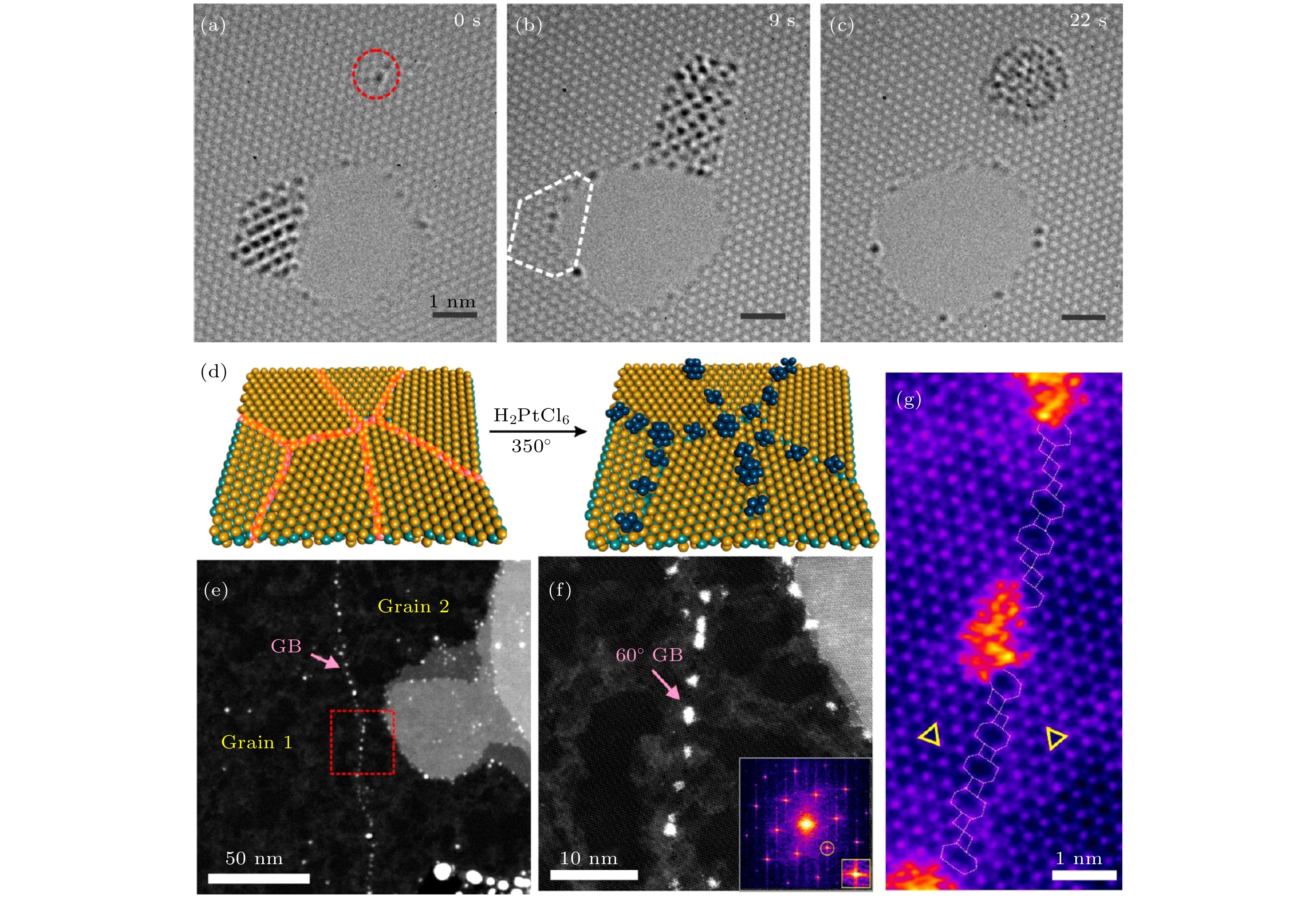
图 1 缺陷和晶界对金属纳米颗粒在二维材料上成核的影响 (a)—(c) AC-TEM图像显示Au纳米团簇在800 ℃下从石墨烯孔的边缘移动到缺陷位置(红色虚线圆圈)[20]; (d)—(g) Pt纳米颗粒在单层MoS2的晶界处选择性成核[24]
Figure 1. Effects of defects and grain boundaries on the nucleation of metal nanoparticles (NPs) on two-dimensional materials: (a)–(c) AC-TEM images at 800 ℃ showing Au clusters moving from the edge of a graphene hole to a defective site (indicated by red dotted circle)[20]; (d)–(g) selective nucleation of Pt NPs at the grain boundary of monolayer MoS2[24].
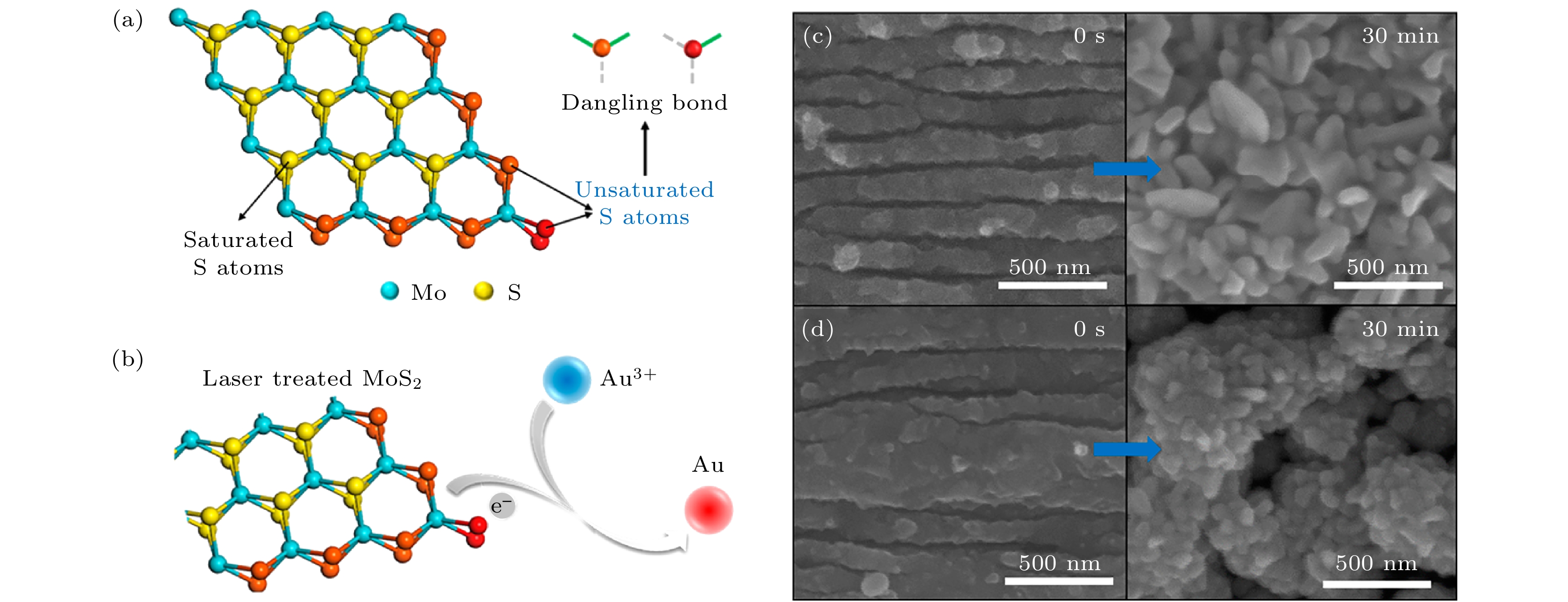
图 2 金纳米颗粒的还原和MoS2表面结构对金纳米颗粒形貌的影响[25] (a)飞秒激光处理后, 在MoS2边缘形成具有S不饱和键的边缘活性位点(红色圆点)的示意图; (b)在边缘活性位点处, 金离子被还原成金原子的示意图; 处理后MoS2表面分别具有(c)短周期结构和(d)长周期结构导致的非球形金纳米颗粒对比图(图中0 s和30 min表示激光处理后的MoS2与AuCl3溶液的反应时间)
Figure 2. Reduction of Au NPs and the effects of surface structures of MoS2 on Au morphology[25]: (a) Schematic of femtosecond pulses irradiating on MoS2; (b) Au cations were reduced to be Au atoms by laser treated MoS2; (c) short-periodic structures and (d) long-periodic structures led to different non-spherical Au NPs (“0 s” and “30 min” represent the reaction time of laser-treated MoS2 and AuCl3 solution).
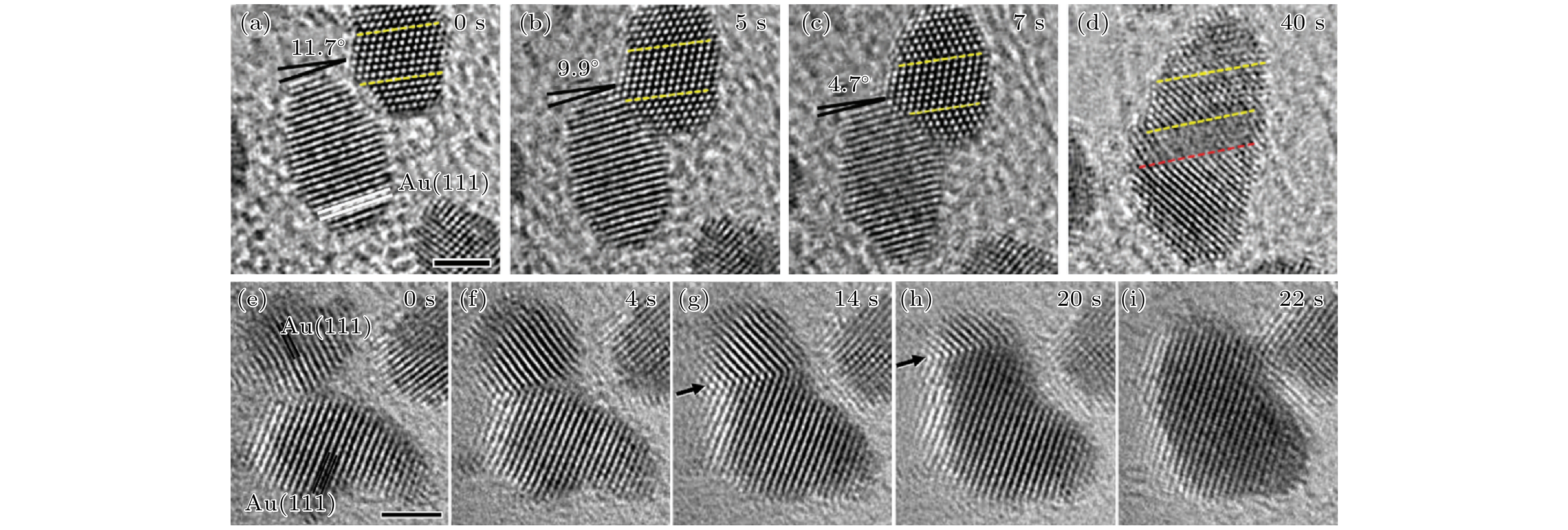
图 3 实时高分辨TEM图像揭示金纳米颗粒通过旋转和晶界推移实现聚合生长过程[33] (a)两个纳米颗粒靠近时的初始位错角为11.7º; (b)—(d)两个纳米颗粒的晶体取向发生旋转, 位错角随时间减小(黄色虚线代表聚合过程中的内部孪晶界, 红色虚线代表聚合后形成的孪晶界); (e)—(f)两个纳米颗粒靠近时在界面处形成高曲率的“颈”状结构; (g)—(i)晶界逐渐推移至聚合颗粒的边缘, 并形成一个单晶颗粒. 标尺为2 nm
Figure 3. Real-time HRTEM images of coalescence of Au NPs via the rotation and grain boundary (GB) migration[33]: (a) Two NPs approach each other with an initial misalignment angle of 11.7º; (b)–(d) the NPs rotate to align their crystallographic orientations (The yellow and red dotted lines indicate the locked and created twin boundaries, respectively, in the combined particle during coalescence); (e)–(f) two NPs come close together and a neck is formed at the particle-particle interface; (g)–(i) GB moves to the edge of the combined particle, creating a single crystalline particle. Scale bar is 2 nm.
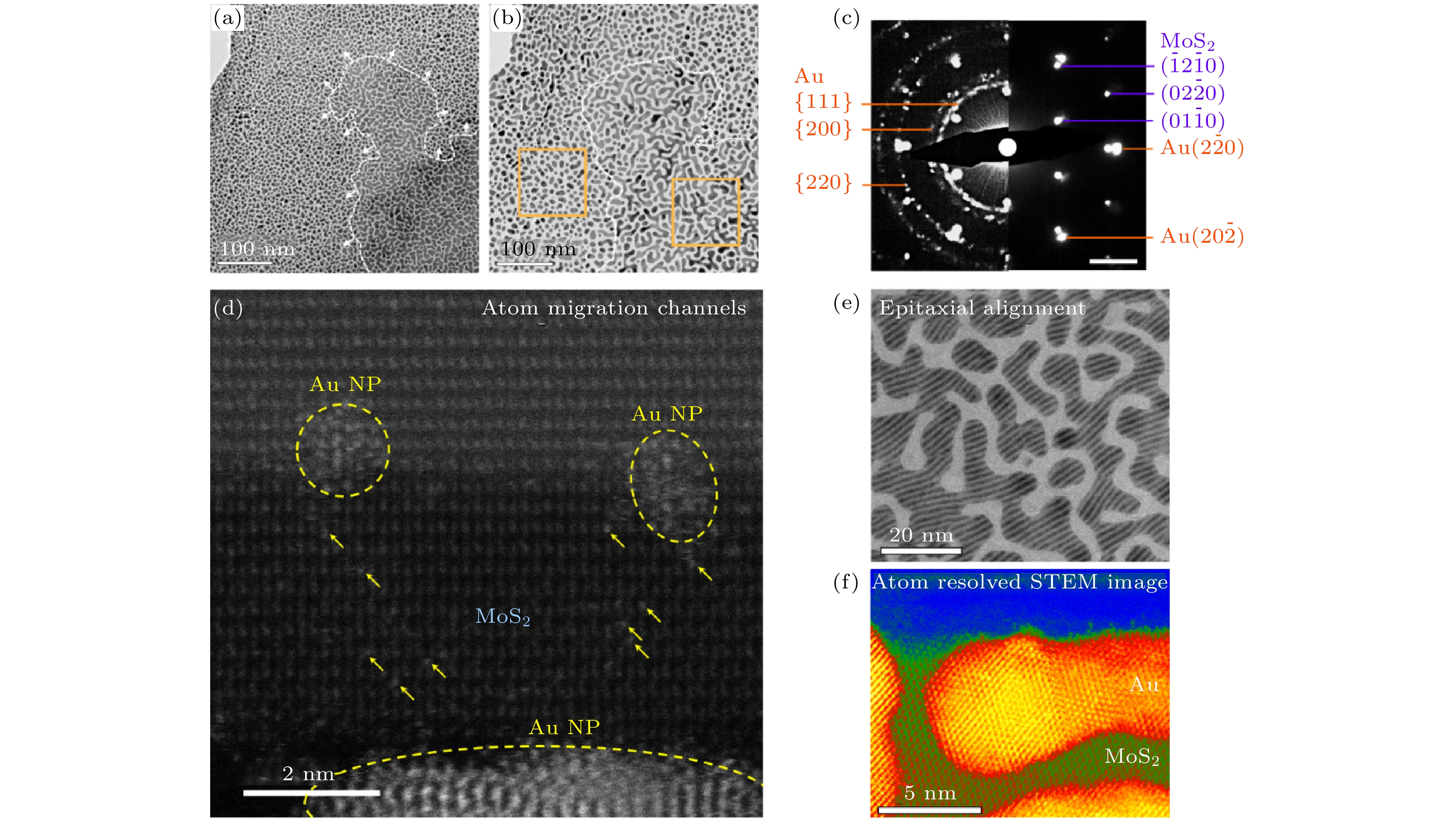
图 4 (a)金刚刚沉积到MoS2上的TEM图像; (b)经过在氮气箱中保存9 d后, 金在MoS2上的TEM图像; (c)图(b)中纳米颗粒区域和枝晶区域的电子衍射图样; (d)原子分辨的STEM图像显示了金原子在MoS2表面上的迁移通道(黄色箭头指示了离散的金原子); (e)金纳米枝晶在MoS2上的典型的莫尔条纹; (f)原子分辨的STEM图像显示了金纳米枝晶与MoS2晶格的外延排列情况[34]
Figure 4. (a) TEM images of Au on MoS2 at the same location just after deposition; (b) TEM images of Au on MoS2 stored in a nitrogen box after 9 days; (c) selective area electron diffraction patterns for the NP and dendrite regions in (b); (d) the atomic-resolution STEM image showing migration channels of Au atoms on MoS2 surfaces (The isolated Au atoms are marked by yellow arrows); (e) typical moiré fringes in HRTEM of Au dendrites on MoS2; (f) the atomic-resolution STEM image showing the lattice match of Au dendrites with MoS2 lattice[34].
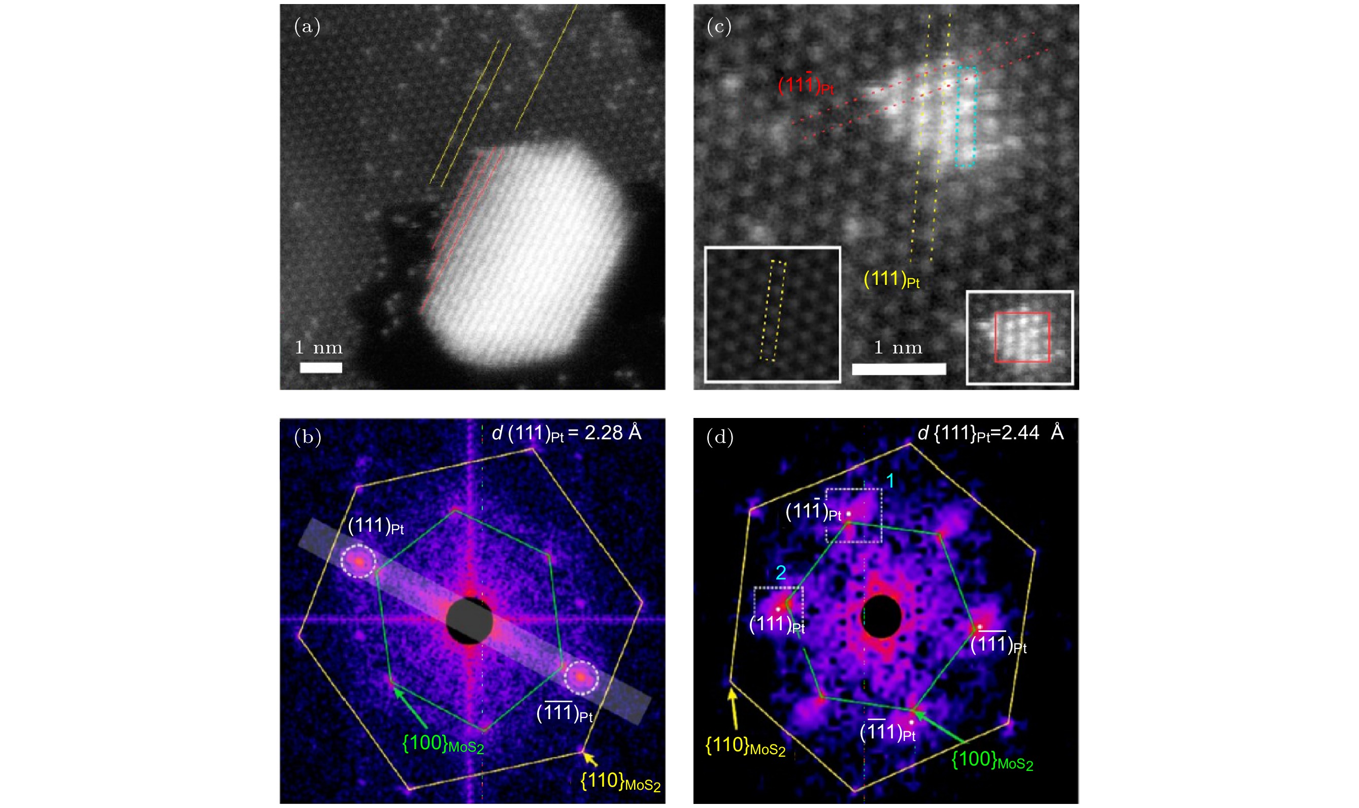
图 5 Pt纳米晶和团簇在MoS2上的晶格取向和晶面间距[23] (a)附着在MoS2边缘上的Pt纳米晶的STEM图像; (b)上面(a)图的FFT图像, 标出了Pt和MoS2的晶面指数, 以及Pt (111)晶面间距; (c)超小的Pt纳米晶或Pt团簇的STEM图像显示了与单层MoS2的外延取向, 左下角插图显示了干净的MoS2区域的STEM图; (d)上面(c)图的FFT图像
Figure 5. Lattice orientation and spacing of Pt nanocrystals and clusters on MoS2[23]: (a) STEM image of a Pt nanocrystal attached to the edge of MoS2; (b) FFT image of (a) with the crystal plane indices of Pt and MoS2, and the crystal plane spacing of Pt (111); (c) STEM image of an ultrasmall Pt nanocrystal or cluster showing the epitaxial orientation on monolayer MoS2 (Inset on the left bottom shows a clean region of MoS2); (d) the FFT image of (c).
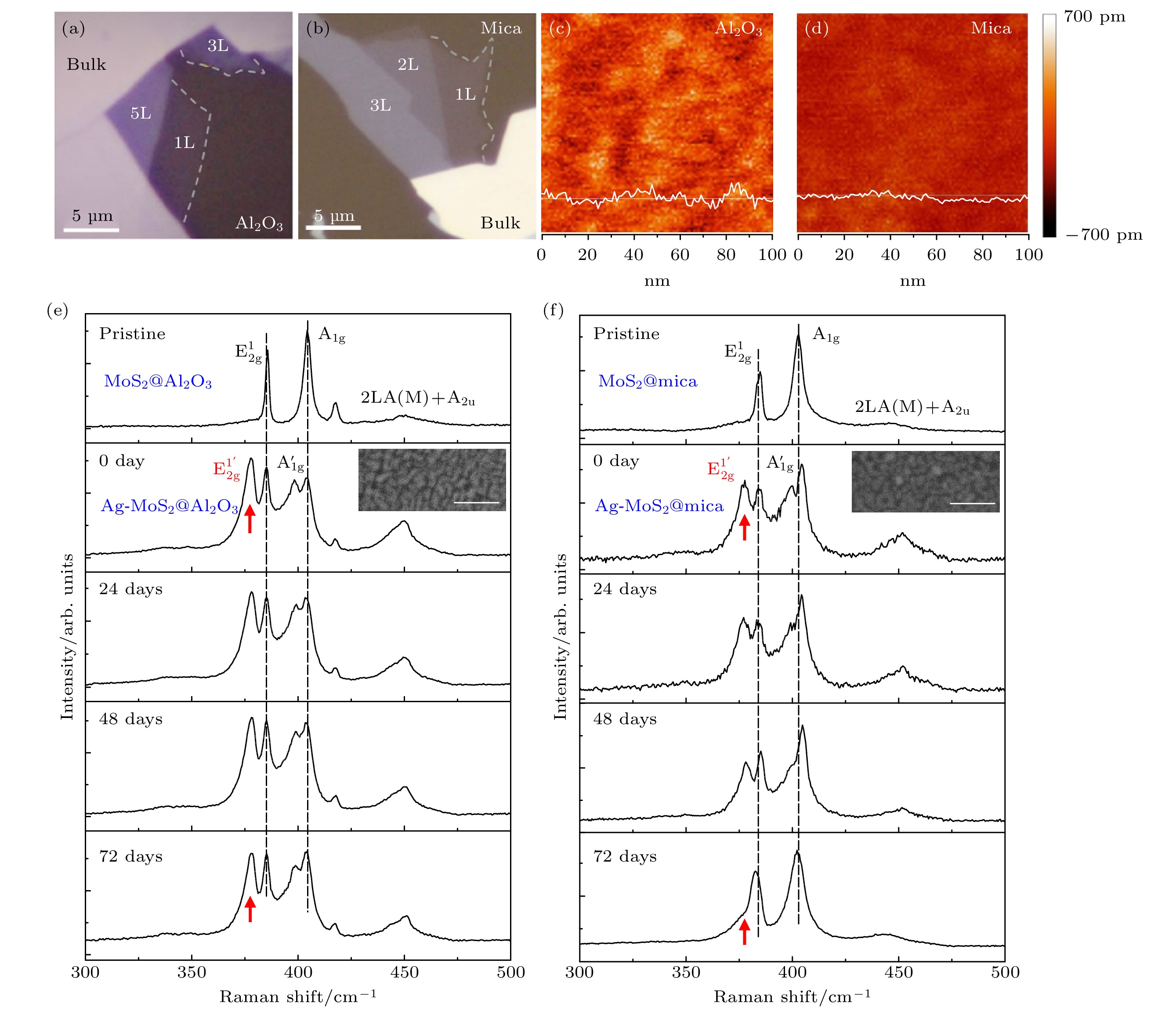
图 6 (a)在Al2O3基底上机械剥离不同层数的MoS2的光学照片; (b)在云母基底上机械剥离不同层数的MoS2的光学照片; (c) Al2O3基底的原子力显微图像; (d) 云母基底的原子力显微图像; (e)在Al2O3基底上的单层MoS2沉积Ag纳米颗粒前后, 以及不同天数的拉曼光谱; (f)在云母基底上的单层MoS2沉积Ag纳米颗粒前后, 以及不同天数的拉曼光谱. 红色箭头分别指示了
${\rm E}_{2\mathrm{g}}^{1'}$ 峰的峰位[49]Figure 6. Optical images of exfoliated MoS2 layers on (a) Al2O3 and (b) mica substrates; AFM images of (c) Al2O3 and (d) mica substrates; comparison of Raman spectra of the pristine and Ag-deposited 1L MoS2 on (e) Al2O3 and (f) mica substrates, as well as the evolution of Raman spectra over time. Raman peak splitting after Ag deposition on the two kinds of substrates can be seen from comparing the first top-most panels and the second panels. The quenching rate of splitting Raman peaks of
${\rm E}_{2\mathrm{g}}^{1'}$ modes differs, as indicated by the red arrows. SEM images of Ag-deposited 1L MoS2 on the two kinds of substrates are shown in the insets. Scale bars are 100 nm[49].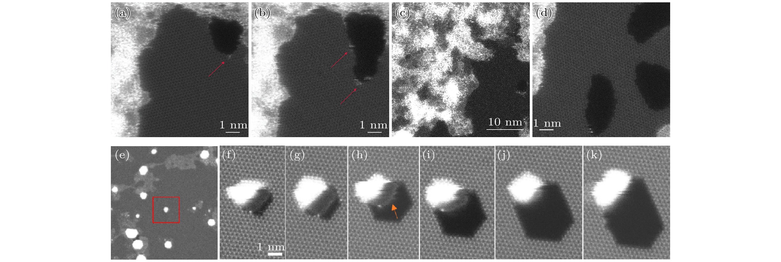
图 7 不同金属团簇刻蚀石墨烯和MoS2的HAADF图像 (a)蒸镀厚度为2 Å的Al以后, 从石墨烯边缘刻蚀出现孔洞的HAADF图像; (b)后续孔洞继续扩大的HAADF图像, 红色箭头标出了一些Al原子; (c)在石墨烯上蒸镀厚度为2 Å的Ti的HAADF图像; (d)由于Ti和石墨烯的相互作用较强, Ti直接从中间区域开始刻蚀[19]; (e) 800 ℃下加热3 h后观察到的还原后的C和Pt纳米晶ADF-STEM图像; (f)—(k)连续ADF-STEM图像显示了图(e)中红色框标示的Pt纳米晶在电子束诱导下对MoS2的反应刻蚀. 橙色箭头表示无定形碳盘. 相邻图的拍照间隔是30 s. 标尺都是1 nm[23]
Figure 7. HAADF images of graphene and MoS2 etched by different metal clusters: (a) Graphene etching in the presence of an Al layer of 2 Å nominal thickness after the start of the hole formation; (b) after the hole enlargement in subsequent scans (Some Al atoms are indicated by red arrows in (a) and (b)); (c) 2 Å titanium evaporated onto monolayer graphene; (d) magnified image showing direct etching of Ti on the basal plane of graphene[19]; (e) ADF-STEM image of a region after 3 h at 800 ℃ showing reduced carbon and Pt nanocrystals; (f)–(k) sequence of ADF-STEM images showing catalytic etching of MoS2 by the Pt nanocrystal labeled in (e), initiated by electron beam irradiation. Orange arrow indicates an amorphous carbon disk. Time between frames is ~30 s. Scale bars are all 1 nm[23].
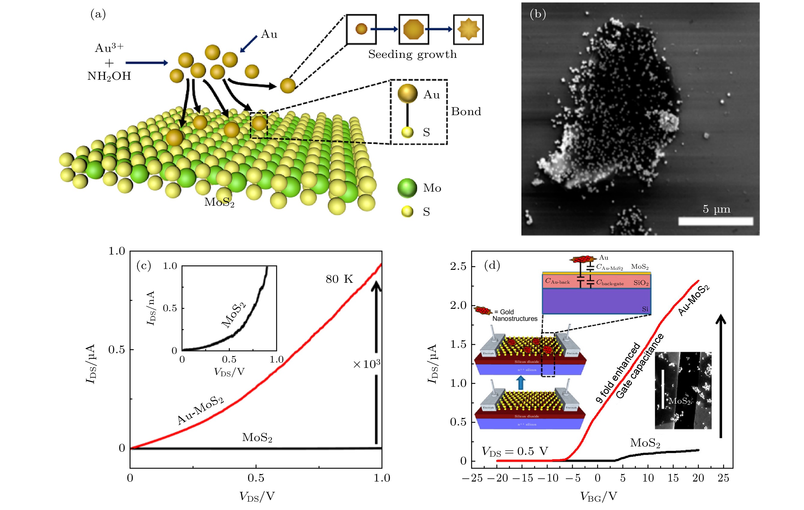
图 8 Au纳米颗粒修饰MoS2的SEM形貌图和对源漏电流的影响[54] (a)通过化学还原法将Au纳米颗粒负载在MoS2上的过程示意图; (b) Au-MoS2杂化体系的SEM图; (c)在80 K下, 负载了Au颗粒以后(Au-MoS2), 器件的电导率增加了103倍(插图显示了80 K下MoS2的输出曲线放大图); (d)在160 K下, 源漏电压为0.5 V时, MoS2和Au-MoS2 FET的背栅调控转移曲线. 插图分别显示了MoS2和Au-MoS2 FETs的结构示意图和等效电容电路图, 以及Au-MoS2 FET器件的SEM图. 标尺为10 μm.
Figure 8. Morphology of MoS2 modified by Au NPs and the effect on source-drain current in FET[54]: (a) Schematic illustration depicting the anchoring of Au NP on MoS2 via chemical reduction strategy; (b) SEM image of Au-MoS2 hybrid structure; (c) at 80 K the conductivity of MoS2 device is increased 103 folds after Au functionalization (Au-MoS2) (The inset shows an enlarged view of IDS versus VDS response for MoS2 at 80 K); (d) at 160 K, with VDS = 0.5 V, back-gating characteristics of MoS2 and Au-MoS2 FETs are shown. The top inset shows capacitance circuitry of the Au-MoS2 device. Bottom-left inset shows the structure of MoS2 FET and Au-MoS2 FET. Bottom-right inset shows a SEM micrograph of Au-MoS2 FET. Scale bar is 10 μm.
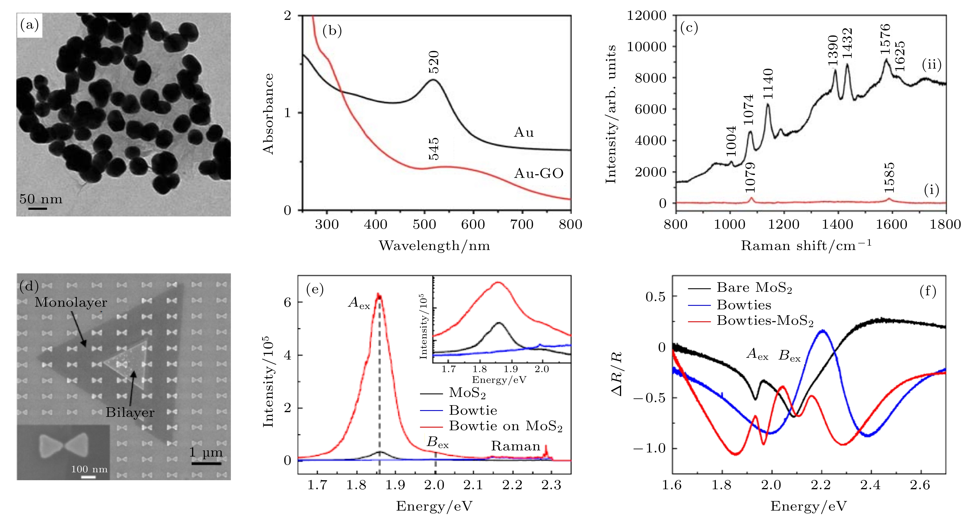
图 9 (a)直径40 nm的Au纳米颗粒附着在GO上的TEM图; (b) Au纳米颗粒在GO上附着前后的水溶液的吸收谱; (c)分别利用Au纳米颗粒(i)和Au-GO复合体系(ii)得到的PATP分子的SERS光谱[63]; (d) Ag领结阵列直接制备在堆叠的单层和双层MoS2三角形薄片上(插图显示了放大后的Ag领结的SEM图); (e)纯MoS2, Ag领结阵列, 以及Ag领结-MoS2的PL光谱对比(插图是对数坐标下的PL光谱数据); (f)在77 K, TE激发极化下, 纯MoS2, Ag领结阵列, 以及Ag领结-MoS2的ΔR/R反射光谱. Ag领结-MoS2体系显示出了由于MoS2激子和LSPR模式光学耦合导致的Fano共振现象. 其中, Ag领结阵列的几何参数: 边长100 nm, x和y方向周期分别为400和300 nm[68]
Figure 9. (a) TEM images of 40 nm Au NPs deposited on GO sheets; (b) UV-vis spectra of aqueous solution of 40 nm Au NPs before and after attachment to the GO sheet; (c) SERS spectra of PATP using (i) the 40 nm Au NPs and (ii) the corresponding Au-GO composites as SERS substrates, respectively[63]; (d) SEM image showing the Ag bowtie array directly patterned on well-defined, stacked triangular flakes of mono- and bilayer MoS2 (The inset shows the enlarged SEM image of the Ag bowtie); (e) PL spectra of bare MoS2, bowtie array and bowtie-MoS2. Inset shows PL in log scale; (f) ΔR/R spectra of bare MoS2, Ag bowtie array, and Ag bowtie-MoS2 at 77 K and TE polarization. Clear Fano resonances are observed when the bowtie lattice-LSP modes overlap with MoS2 excitons. Ag bowtie array: side length 100 nm, x and y direction periods 400 and 300 nm, respectively[68].
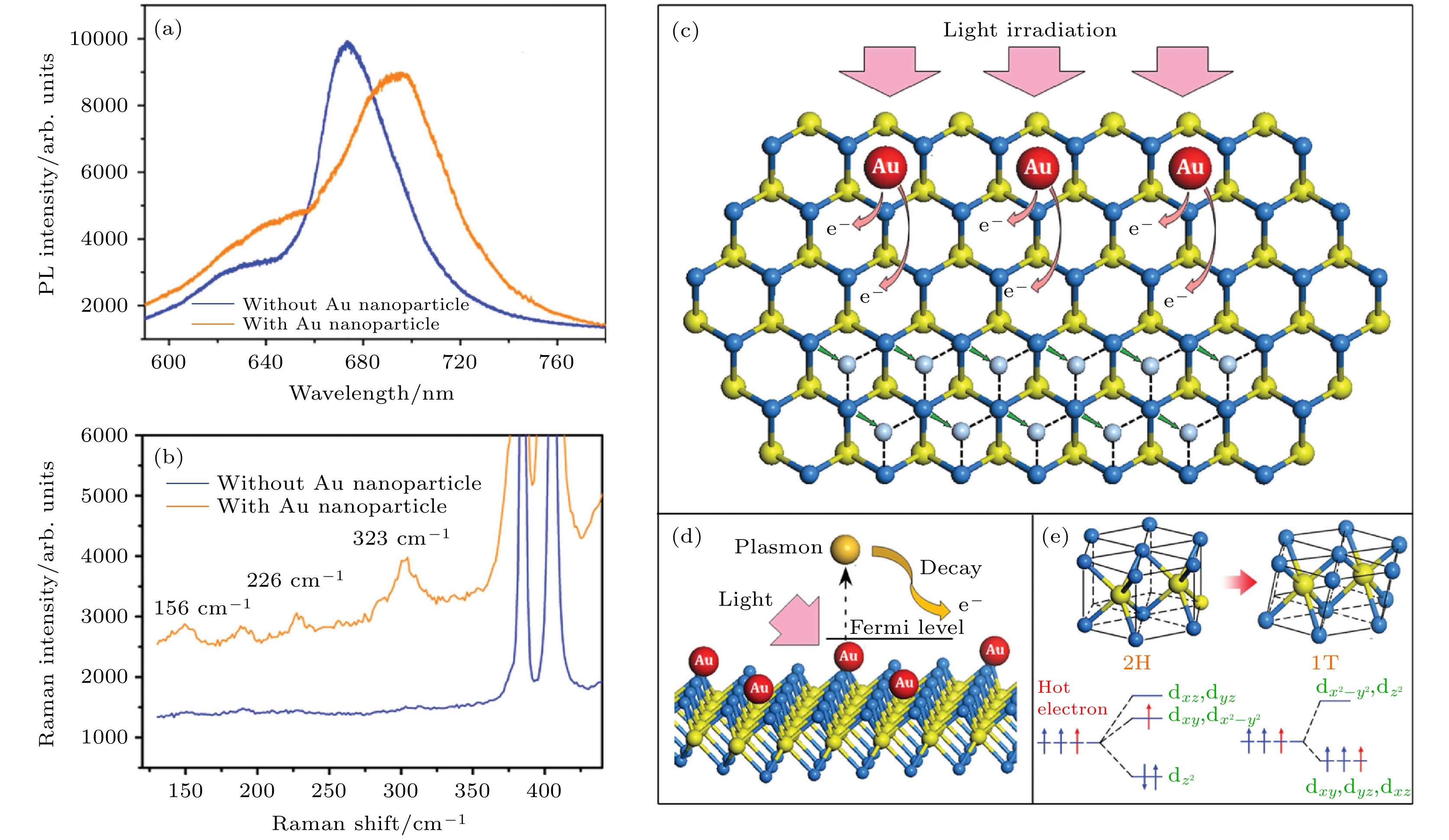
图 10 表面等离激元共振产生的热电子诱导MoS2单层从2H相到1T相相变[84] (a)在MoS2上沉积直径5 nm的金纳米颗粒后, PL光谱出现红移和展宽; (b)在Au纳米颗粒沉积后出现的三个新的拉曼峰与1T相一致; (c) MoS2薄膜的示意图, 其中Au纳米颗粒产生的热电子转移到MoS2中; (d) Au纳米颗粒中的等离激元衰减成热电子, 其最高的电子能量在费米能级以上一个等离激元量子(热电子产生的原理), 而热电子可以转移到MoS2的导带中; (e) 2H和1T晶格结构之间的转变(在晶体配位场理论中, 2H相中的Mo 4d轨道具有3个能级, 而1T中的Mo 4d轨道仅具有2个能级. 当热电子填充未占据的Mo 4d轨道时, 1T相稳定)
Figure 10. Plasmonic hot electron induced structural phase transition from 2H to 1T in monolayer MoS2[84]: (a) PL spectrum red-shifting and broadening was found after the 5 nm Au NPs were deposited on MoS2; (b) three new Raman peaks consistent with the 1T phase recorded after the Au NP deposition; (c) schematic of a MoS2 film with hot electrons generated from Au NPs; (d) the principle of hot electron generation is Au NP plasmon decay into hot electrons with the highest electron energies one plasmon quantum above the Fermi level; (e) the transition between 2H and 1T structure (The Mo 4d-orbitals in 2H phase have three groups, and in 1T phase have two. When an extra electron fill an unoccupied Mo 4d-orbital, the 1T phase is stabilized).
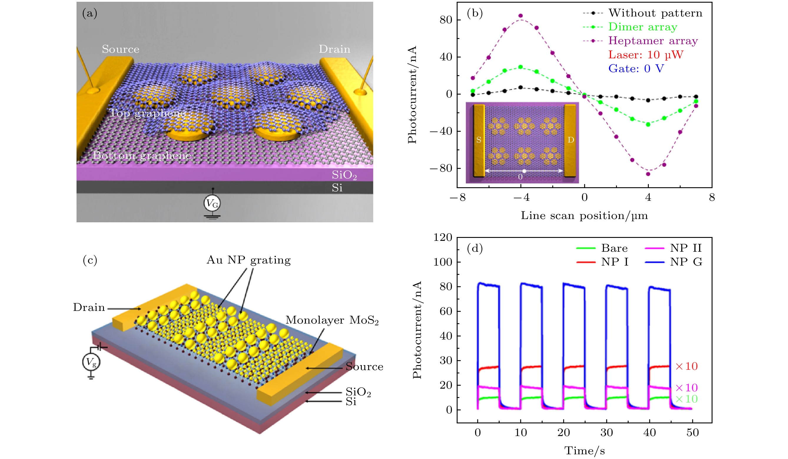
图 11 (a)夹在两片单层石墨烯之间的单个Au纳米盘七聚体的示意图; (b)沿着插图中所示的线扫描方向, 对没有Au纳米天线、有Au纳米盘二聚体和七聚体阵列修饰的石墨烯的光电流的测量结果[95]; (c)负载Au纳米颗粒光栅结构的单层MoS2光电探测器的示意图; (d)不同光电探测器的光电流随时间的变化曲线, 其中VG = 0 V, VDS = 1 V. Bare表示没有Au纳米颗粒负载的单层MoS2, NP I和NP II分别表示MoS2上负载的Au纳米颗粒具有不同的直径和密度, NP G表示Au纳米颗粒光栅结构[73]
Figure 11. (a) Schematic illustration of a single Au heptamer sandwiched between two sheets of monolayer graphene; (b) photocurrent measurements of graphene without Au nanoantennas and modified by Au dimer and heptamer arrays, obtained along the line scan direction shown in the inset; (c) schematic diagram of a monolayer MoS2 photodetector loaded with Au NP grating; (d) photocurrent-time response of different photodetectors, where VG = 0 V and VDS = 1 V. Bare denotes monolayer MoS2 without Au NPs, NP I and NP II denote Au NPs loaded on MoS2 with different diameters and densities, respectively, and NP G denotes Au NP grating structure[73].
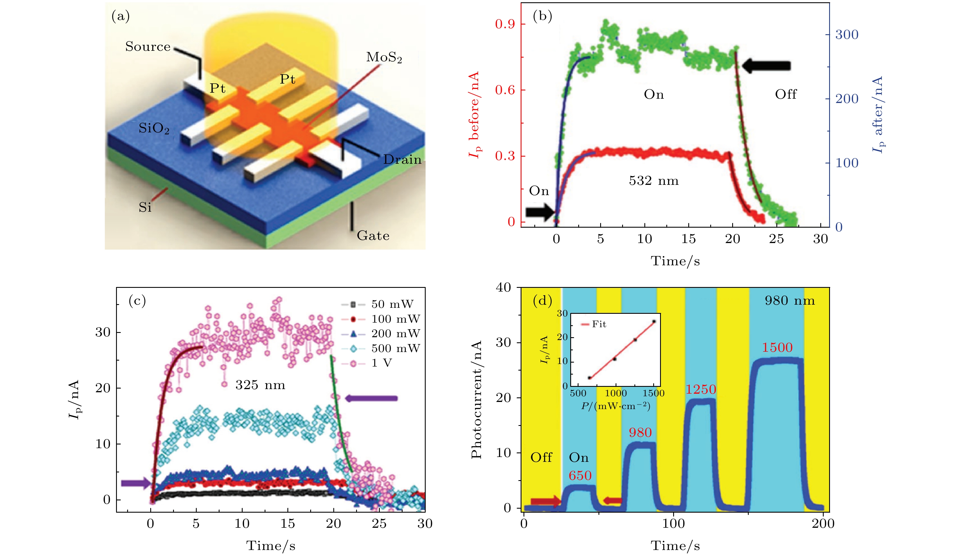
图 12 (a)修饰有Pt纳米带的双层MoS2光电器件示意图; (b)在可见光(532 nm)照射下, 测量沉积Pt纳米带前后器件光电流随时间的变化(红色表示沉积前的结果, 绿色表示沉积后的结果); (c)在紫外光(325 nm)照射下, 测量不同偏置电压下的光电流随时间的变化(光功率密度: 184 mW·cm–2); (d)在近红外光(980 nm)照射下, 改变入射光功率密度, 测得的时间依赖的光电流曲线(偏置电压: 1 V). 插图显示光电流正比于入射激光功率[96]
Figure 12. (a) Schematic diagram of a bilayer MoS2 device deposited with Pt nanostrips; (b) time-dependent photocurrent measurement before and after deposition of Pt nanostrips under visible light (532 nm) irradiation (Red curve indicates the result before deposition and green curve indicates that after deposition); (c) photocurrent measurement at different bias voltages under UV light (325 nm) irradiation (power density 184 mW·cm–2); (d) time-dependent photocurrent measurements under exposure to different NIR light (980 nm) intensities (bias voltage: 1 V), where the inset shows that the linear dependence of the photocurrent on the incident laser power intensity[96].
-
[1] Geim A K, Novoselov K S 2007 Nat. Mater. 6 183
Google Scholar
[2] Chen J H, Jang C, Xiao S, Ishigami M, Fuhrer M S 2008 Nat. Nanotechnol. 3 206
Google Scholar
[3] Balandin A A, Ghosh S, Bao W, Calizo I, Teweldebrhan D, Miao F, Lau C N 2008 Nano Lett. 8 902
Google Scholar
[4] Lee C, Wei X, Kysar J W, Hone J 2008 Science 321 385
Google Scholar
[5] Panchokarla L S, Subrahmanyam K S, Saha S K, Govindaraj A, Krishnamurthy H R, Waghmare U V, Rao C N R 2009 Adv. Mater. 21 4726
[6] Wei D, Liu Y, Wang Y, Zhang H, Huang L, Yu G 2009 Nano Lett. 9 1752
Google Scholar
[7] Latorre-Sanchez M, Primo A, Garcia H 2013 Angew. Chem. Int. Edit. 52 11813
Google Scholar
[8] Jiao L, Zhang L, Wang X, Diankov G, Dai H 2009 Nature 458 877
Google Scholar
[9] Jiao L, Wang X, Diankov G, Wang H, Dai H 2010 Nat. Nanotechnol. 5 321
Google Scholar
[10] Radisavljevic B, Radenovic A, Brivio J, Giacometti V, Kis A 2011 Nat. Nanotechnol. 6 147
Google Scholar
[11] Wang Q H, Kalantar-Zadeh K, Kis A, Coleman J N, Strano M S 2012 Nat. Nanotechnol. 7 699
Google Scholar
[12] Mak K F, Shan J 2016 Nat. Photonics 10 216
Google Scholar
[13] Lü R, Terrones H, Elias A L, Perea-Lopez N, Gutierrez H R, Cruz-Silva E, Rajukumar L P, Dresselhaus M S, Terrones M 2015 Nano Today 10 559
Google Scholar
[14] Tan C L, Cao X H, Wu X J, He Q Y, Yang J, Zhang X, Chen J Z, Zhao W, Han S K, Nam G H, Sindoro M, Zhang H 2017 Chem. Rev. 117 6225
Google Scholar
[15] Zhou L, Xia T, Cao T, Wang L, Chen Y, Li S, Wang R, Guo H 2020 J. Alloys Compd. 818 152909
Google Scholar
[16] Najmaei S, Mlayah A, Arbouet A, Girard C, Leotin J, Lou J 2014 ACS Nano 8 12682
Google Scholar
[17] Xiu X W, Zhang W C, Hou S T, Li Z, Lei F C, Xu S C, Li C H, Man B Y, Yu J, Zhang C 2021 Chin. Phys. B 30 088801
Google Scholar
[18] Zan R, Bangert U, Ramasse Q, Novoselov K S 2011 Small 7 2868
Google Scholar
[19] Zan R, Bangert U, Ramasse Q, Novoselov K S 2012 J. Phys. Chem. Lett. 3 953
Google Scholar
[20] Chen Q, He K, Robertson A W, Kirkland A I, Warner J H 2016 ACS Nano 10 10418
Google Scholar
[21] Zhou H, Yu F, Guo C F, Wang Z, Lan Y, Wang G, Fang Z, Liu Y, Chen S, Sun L F, Ren Z 2015 Nanoscale 7 9153
Google Scholar
[22] Jin Z, Nackashi D, Lu W, Kittrell C, Tour J M 2010 Chem. Mater. 22 5695
Google Scholar
[23] Wang S, Sawada H, Chen Q, Han G G D, Allen C, Kirkland A I, Warner J H 2017 ACS Nano 11 9057
Google Scholar
[24] Wang S, Sawada H, Han X, Zhou S, Li S, Guo Z X, Kirkland A I, Warner J H 2018 ACS Nano 12 5626
Google Scholar
[25] Zuo P, Jiang L, Li X, Li B, Xu Y, Shi X, Ran P, Ma T, Li D, Qu L, Lu Y, Grigoropoulos C P 2017 ACS Appl. Mater. Interfaces 9 7447
Google Scholar
[26] Lei Y T, Li D W, Zhang T C, Huang X, Liu L, Lu Y F 2017 J. Mater. Chem. C 5 8883
Google Scholar
[27] Liu X W, Wang D S, Li Y D 2012 Nano Today 7 448
Google Scholar
[28] Huang X, Li S, Wu S, Huang Y, Boey F, Gan C L, Zhang H 2012 Adv. Mater. 24 979
Google Scholar
[29] Kidd T E, Weber J, Holzapfel R, Doore K, Stollenwerk A J 2018 Appl. Phys. Lett. 113 191603
Google Scholar
[30] Muszynski R, Seger B, Kamat P V 2008 J. Phys. Chem. C 112 5263
Google Scholar
[31] Kamat P V 2010 J. Phys. Chem. Lett. 1 520
Google Scholar
[32] Li Y, Fan X, Qi J, Ji J, Wang S, Zhang G, Zhang F 2010 Nano Res. 3 429
Google Scholar
[33] Yuk J M, Jeong M, Kim S Y, Seo H K, Kim J, Lee J Y 2013 Chem. Commun. 49 11479
Google Scholar
[34] Sun Y, Zhao H, Zhou D, Zhu Y, Ye H, Moe Y A, Wang R 2019 Nano Res. 12 947
Google Scholar
[35] Lu X, Luo X, Zhang J, Quek S Y, Xiong Q 2016 Nano Res. 9 3559
Google Scholar
[36] Wu J B, Lin M L, Cong X, Liu H N, Tan P H 2018 Chem. Soc. Rev. 47 1822
Google Scholar
[37] Lee C, Yan H, Brus L E, Heinz T F, Hone J, Ryu S 2010 ACS Nano 4 2695
Google Scholar
[38] Liu H T, Ryu S M, Chen Z Y, Steigerwald M L, Nuckolls C, Brus L E 2009 J. Am. Chem. Soc. 131 17099
Google Scholar
[39] Martins F E H, Moutinho M V O, Stavale F, Lucchese M M, Capaz R B, Achete C A, Jorio A 2010 Phys. Rev. B 82 125429
Google Scholar
[40] Lui C H, Malard L M, Kim S, Lantz G, Laverge F E, Saito R, Heinz T F 2012 Nano Lett. 12 5539
Google Scholar
[41] Wu J B, Zhang X, Ijaes M, Han W P, Qiao X F, Li X L, Jiang D S, Ferrari A C, Tan P H 2014 Nat. Commun. 5 5309
Google Scholar
[42] Zhang X, Han W P, Qiao X F, Tan Q H, Wang Y F, Zhang J, Tan P H 2016 Carbon 99 118
Google Scholar
[43] Zhang X, Han W P, Wu J B, Milana S, Lu Y, Li Q Q, Ferrari A C, Tan P H 2013 Phys. Rev. B 87 115413
Google Scholar
[44] Zhao H, Wu J B, Zhong H X, Guo Q S, Wang X M, Xia F N, Yang L, Tan P H, Wang H 2015 Nano Res. 8 3651
Google Scholar
[45] Liu K, Zhang L, Cao T, Jin C, Qiu D, Zhou Q, Zettl A, Yang P, Louie S G, Wang F 2014 Nat. Commun. 5 4966
Google Scholar
[46] Wang P, Zhang D, Zhang L, Fang Y 2013 Chem. Phys. Lett. 556 146
Google Scholar
[47] Qiu C, Zhou H, Cao B, Sun L, Yu T 2013 Carbon 59 487
Google Scholar
[48] Gong C, Huang C, Miller J, Cheng L, Hao Y, Cobden D, Kim J, Ruoff R S, Wallace R M, Cho K, Xu X, Chabal Y J 2013 ACS Nano 7 11350
Google Scholar
[49] Sun Y, Moe Y A, Xu Y, Sun Y, Wang X, Li F, Liu K, Wang R 2019 Nanoscale 11 22432
Google Scholar
[50] Sun Y H, Liu K, Hong X P, Chen M, Kim J, Shi S F, Wu J Q, Zettl A, Wang F 2014 Nano Lett. 14 5329
Google Scholar
[51] Moe Y A, Sun Y H, Ye H Y, Liu K, Wang R 2018 ACS Appl. Mater. Interfaces 10 40246
Google Scholar
[52] Boukhvalov D W, Katsnelson M I 2009 Appl. Phys. Lett. 95 023109
[53] Campos L C, Manfrinato V R, Sanchez-Yamagishi J D, Kong J, Jarillo-Herrero P 2009 Nano Lett. 9 2600
Google Scholar
[54] Sreeprasad T S, Phong N, Kim N, Berry V 2013 Nano Lett. 13 4434
Google Scholar
[55] Chen C H, Wu C L, Pu J, Chiu M H, Kumar P, Takenobu T, Li L J 2014 2D Mater. 1 034001
[56] Shi Y, Huang J K, Jin L, Hsu Y T, Yu S F, Li L J, Yang H Y 2013 Sci. Rep. 3 1839
Google Scholar
[57] Li W W, Geng X M, Guo Y F, Rong J Z, Gong Y P, Wu L Q, Zhang X M, Li P, Xu J B, Cheng G S, Sun M T, Liu L W 2011 ACS Nano 5 6955
Google Scholar
[58] He Q, Zeng Z, Yin Z, Li H, Wu S, Huang X, Zhang H 2012 Small 8 2994
Google Scholar
[59] Chen K, Lu G, Chang J, Mao S, Yu K, Cui S, Chen J 2012 Anal. Chem. 84 4057
Google Scholar
[60] Xu W G, Mao N N, Zhang J 2013 Small 9 1206
Google Scholar
[61] Jing X X, Li D Q, Zhang Y, Hou X Y, Jiang J, Fan X C, Wang M C, Feng S P, Yu Y F, Lu J P, Hu Z L, Ni Z H 2021 Chin. Phys. Lett. 38 074203
Google Scholar
[62] Li J H, Zhang S N, Zhai Y J, Ma J G, Fang W H, Zhang Y 2019 Acta Phys. Sin. 68 134203
Google Scholar
[63] Huang J, Zhang L, Chen B, Ji N, Chen F, Zhang Y, Zhang Z 2010 Nanoscale 2 2733
Google Scholar
[64] Hou H, Wang P, Zhang J, Li C, Jin Y 2015 ACS Appl. Mater. Interfaces 7 18038
Google Scholar
[65] Liu M, Chen W 2013 Biosens. Bioelectron. 46 68
Google Scholar
[66] Gupta S, Banaszak A, Smith T, Dimakis N 2018 J. Raman Spectrosc. 49 438
Google Scholar
[67] Singha S S, Nandi D, Singha A 2015 RSC Adv. 5 24188
Google Scholar
[68] Lee B, Park J, Han G H, Ee H S, Naylor C H, Liu W, Johnson A T C, Agarwal R 2015 Nano Lett. 15 3646
Google Scholar
[69] Mak K F, Lee C, Hone J, Shan J, Heinz T F 2010 Phys. Rev. Lett. 105 136805
Google Scholar
[70] Lee K C J, Chen Y H, Lin H Y, Cheng C C, Chen P Y, Wu T Y, Shih M H, Wei K H, Li L J, Chang C W 2015 Sci. Rep. 5 16374
Google Scholar
[71] Butun S, Tongay S, Aydin K 2015 Nano Lett. 15 2700
Google Scholar
[72] Sobhani A, Lauchner A, Najmaei S, Ayala-Orozco C, Wen F, Lou J, Halas N J 2014 Appl. Phys. Lett. 104 031112
Google Scholar
[73] Li J, Nie C, Sun F, Tang L, Zhang Z, Zhang J, Zhao Y, Shen J, Feng S, Shi H, Wei X 2020 ACS Appl. Mater. Interfaces 12 8429
Google Scholar
[74] Gao W, Lee Y H, Jiang R, Wang J, Liu T, Ling X Y 2016 Adv. Mater. 28 701
Google Scholar
[75] Zhang H Z, Xu C Y, Nan H Y, Xiao S Q, Gu X F 2020 Acta Phys. Sin. 69 246101
Google Scholar
[76] Chi Z H, Zhao X M, Zhang H, Goncharov A F, Lobanov S S, Kagayama T, Sakata M, Chen X J 2014 Phys. Rev. Lett. 113 036802
Google Scholar
[77] Nayak A P, Bhattacharyya S, Zhu J, Liu J, Wu X, Pandey T, Jin C, Singh A K, Akinwande D, Lin J F 2014 Nat. Commun. 5 3731
Google Scholar
[78] Liu B, Han Y H, Gao C X, Ma Y Z, Peng G, Wu B J, Liu C L, Wang Y, Hu T J, Cui X Y, Ren W B, Li Y, Su N N, Liu H W, Zou G T 2010 J. Phys. Chem. C 114 14251
Google Scholar
[79] Lin Y C, Dumcencon D O, Huang Y S, Suenaga K 2014 Nat. Nanotechnol. 9 391
Google Scholar
[80] Loh T A J, Chua D H C 2015 J. Phys. Chem. C 119 27496
Google Scholar
[81] Py M A H, Haering R R 1983 Can. J. Phys. 61 76
Google Scholar
[82] Wang L, Xu Z, Wang W, Bai X D 2014 J. Am. Chem. Soc. 136 6693
Google Scholar
[83] Wang X F, Shen X, Wang Z X, Yu R C, Chen L Q 2014 ACS Nano 8 11394
Google Scholar
[84] Kang Y, Najmaei S, Liu Z, Bao Y, Wang Y, Zhu X, Halas N J, Nordlander P, Ajayan P M, Lou J, Fang Z Y 2014 Adv. Mater. 26 6467
Google Scholar
[85] Gong C, Zhang H J, Wang W H, Colombo L, Wallace R M, Cho K J 2013 Appl. Phys. Lett. 103 053513
Google Scholar
[86] Kang Y, Gong Y, Hu Z, Li Z, Qiu Z, Zhu X, Ajayan P M, Fang Z 2015 Nanoscale 7 4482
Google Scholar
[87] Wei S, Cui X Q, Xu Y, Shang B, Zhang Q, Gu L, Fan X, Zheng L, Hou C, Huang H, Wen S, Zheng W T 2019 ACS Energy Lett. 4 368
Google Scholar
[88] Shang B, Cui X Q, Jiao L, Qi K, Wang Y W, Fan J C, Yue Y Y, Wang H Y, Bao Q L, Fan X F, Wei S T, Song W, Cheng Z L, Guo S J, Zheng W T 2019 Nano Lett. 19 2758
Google Scholar
[89] Qi K, Cui X Q, Gu L, Yu S, Fan X, Luo M, Xu S, Li N, Zheng L, Zhang Q, Ma J, Gong Y, Lü F, Wang K, Huang H, Zhang W, Guo S, Zheng W T, Liu P 2019 Nat. Commun. 10 5231
Google Scholar
[90] Miao J, Hu W, Jing Y, Luo W, Liao L, Pan A, Wu S, Cheng J, Chen X, Lu W 2015 Small 11 2392
Google Scholar
[91] Lan H Y, Hsieh Y H, Chiao Z Y, Jariwala D, Shih M H, Yen T J, Hess O, Lu Y J 2021 Nano Lett. 21 3083
Google Scholar
[92] Chen W, Liang R, Liu Y, Zhang S, Cheng W, Zhao L, Xu J 2019 Appl. Phys. Lett 115 142102
Google Scholar
[93] Han X, Xing J, Xu H, Huang Y, Li D, Lu J, Li P, Wu Y 2020 Nanotechnology 31 215201
Google Scholar
[94] Sriram P, Wen Y P, Manikandan A, Hsu K C, Tang S Y, Hsu B W, Chen Y Z, Lin H W, Jeng H T, Chueh Y L, Yen T J 2020 Chem. Mater. 32 2242
Google Scholar
[95] Fang Z Y, Liu Z, Wang Y, Ajayan P M, Nordlander P, Halas N J 2012 Nano Lett. 12 3808
Google Scholar
[96] Kumar R, Sharma A, Kaur M, Husale S 2017 Adv. Opt. Mater 5 1700009
Google Scholar

 DownLoad:


Catalog
Metrics
- Abstract views: 7690
- PDF Downloads: 366
- Cited By: 0
