


-
Although graphene-based heterostructures exhibit excellent intrinsic properties for device scaling, fabricating low Schottky barrier is still a great challenge to the electrical transport behaviors of nanoelectronic devices. Exploring excellent materials for electronic devices are a research hotspot at present. Graphene not only exhibits excellent physical strength and specific surface area, but also presents high carrier mobility and thermal conductivity. Therefore, graphene has been developed in many fields such as energy, catalysis, etc. However, graphene is a special material with zero band gap, and its electrons and holes are easy to compound, which seriously hinders its development in the applications of electronic and optoelectronic devices. Two-dimensional transition metal dichalcogenides (TMDs) have the advantages of controllable band gap properties, which makes them have a good development in logic circuits and photodetectors. As one of TMDS, MoSe2 possesses the advantages of narrower band gap, better electron hole separation and stronger oxidation resistance in the environment. Therefore, the design of graphene and MoSe2 heterostructures is an ideal choice for a new generation of nanoelectronic devices. Here, we investigate systematically the effects of asymmetric O doping on the electronic properties and Schottky barrier of graphene/MoSe2(1–x)O2x heterostructure for the first time by first-principles calculations incorporating semiempirical dispersion-correction scheme. The results indicate that graphene and MoSe2 monolayer can form a stable van der Waals heterostructure with preserving their own intrinsic properties. In addition, an n-type schottky contact with a barrier height of 0.558 eV is obtained. Further, it is found that the type and the height of the Schottky barrier can be controlled by changing the concentration and sites of the O dopant at interface. By increasing the concentration of the O dopant inside the interface, the transition from an n-type Schottky contact to an Ohmic contact can be realized, and a low n-type Schottky barrier is gained with increasing the concentration of the O dopant outside the interface for highly efficient charge transfer. The barrier height of heterostructure decreases from 0.558 eV to 0.112 eV when the O dopant is doped on the outer interface. Finally, as a complement to previous results, it is confirmed that the redistribution of interfacial charges leads the Fermi level to shift, and thus determining the type and the height of Schottky barrier. This study may provide theoretical guidance for designing and manufacturing the MoSe2-based nano field effect transistors.
-
Keywords:
- heterostructure /
- density functional theory /
- asymmetric doping /
- Schottky barrier
[1] Geim A K 2009 Science 324 1530
 Google Scholar
[2] Novoselov K S, Jiang Z, Zhang Y, et al. 2007 Science 315 1379
Google Scholar
[3] Tonndorf P, Schmidt R, Böttger P, et al. 2013 Opt. express 21 4908
Google Scholar
[4] Rathi S, Lee I, Lim D, Wang J, Ochiai Y, Aoki N, Watanabe K, Taniguchi T, Lee G H, Yu Y J, Kim P, Kim G H 2015 Nano Lett. 15 5017
Google Scholar
[5] Ross J S, Wu S, Yu H, Ghimire N J, Jones A M, Aivazian G, Yan J, Mandrus D G, Xiao D, Yao W, Xu X 2013 Nat. Commun. 4 1474
Google Scholar
[6] Tongay S, Zhou J, Ataca C, Lo K, Matthews T S, Li J, Grossman J C, Wu J 2012 Nano Lett. 12 5576
Google Scholar
[7] Larentis S, Fallahazad B, Tutuc E 2012 Appl. Phys. Lett. 101 223104
Google Scholar
[8] Liu Y, Guo J, Zhu E, Liao L, Lee S J, Ding M, Shakir I, Gambin V, Huang Y, Duan X 2018 Nature 557 696
Google Scholar
[9] Bardeen J 1947 Phys. Rev. 71 717
Google Scholar
[10] Miedema A R, Chatel P F, Boer F R 1980 Physica 100 1
Google Scholar
[11] Çakır D, Sevik C, Peeters F 2014 J. Mater. Chem. C 2 9842
Google Scholar
[12] Hong X, Kim J, Shi S F, Zhang Y, Jin C, Sun Y, Tongay S, Wu J, Zhang Y, Wang F 2014 Nat. Nanotechnol. 9 682
Google Scholar
[13] Vu T V, Hieu N V, Phuc H V, Hieu N N, Bui H D, Idrees M, Amin B, Nguyen C V 2020 Appl. Surf. Sci. 507 145036
Google Scholar
[14] 郭丽娟, 胡吉松, 马新国, 项炬 2019 物理学报 68 097101
Google Scholar
Guo L J, Hu J S, Ma X G, Xiang J 2019 Acta Phys. Sin. 68 097101
Google Scholar
[15] Sata Y, Moriya R, Morikawa S, Yabuki N, Masubuchi S, Machida T 2015 Appl. Phys. Lett. 107 023109
Google Scholar
[16] Sun Z, Chu H, Li Y, Zhao S, Li G, Li D 2019 Mater. Design 183 108129
Google Scholar
[17] Hu J, Duan W, He H, Lv H, Huang C, Ma X 2019 J. Mater. Chem. C 7 7798
Google Scholar
[18] Weng J, Gao S P 2018 Phys. Chem. Chem. Phys. 20 26453
Google Scholar
[19] Perdew J, Burke K, Ernzerhof M 1996 Phys. Rev. Lett. 77 3865
Google Scholar
[20] Tkatchenko A, Scheffler M 2009 Phys. Rev. Lett. 102 073005
Google Scholar
[21] Chan K, Neaton J, Cohen M 2008 Phys. Rev. B 77 235430
Google Scholar
[22] Saha P, Ghosh B, Mazumder A, Mukherjee G D 2020 Mater. Res. Express 7 025902
Google Scholar
[23] Zhang R, Hao G, Ye X, Gao S, Li H 2020 Phys. Chem. Chem. Phys. 22 23699
Google Scholar
[24] Hieu N N, Phuc H V, Ilyasov V V, Chien N D, Poklonski N A, Van Hieu N, Nguyen C V 2017 J. Appl. Phys. 122 104301
Google Scholar
[25] Hu J, Ji G, Ma X, He H, Huang C 2018 Appl. Surf. Sci. 440 35
Google Scholar
[26] Zhang R, Hao G, Li H, Ye X, Gao S, Yuan X, Liu C 2020 J. Phys. Chem. Solids 143 109466
Google Scholar
[27] Peng Q, Wang Z, Sa B, Wu B, Sun Z 2016 Sci. Rep-UK 6 31994
Google Scholar
[28] Ugeda M, Bradley A, Shi S F, Da Jornada F, Zhang Y, Qiu D, Mo S K, Hussain Z, Shen Z X, Wang F, Louie S, Crommie M 2014 Nat. Mater. 13 1091
Google Scholar
[29] 危阳, 马新国, 祝林, 贺华, 黄楚云 2017 物理学报 66 087101
Google Scholar
Wei Y, Ma X G, Zhu L, He H, Huang C Y 2017 Acta Phys. Sin. 66 087101
Google Scholar
[30] Bjorkman T, Gulans A, Krasheninnikov A V, Nieminen R M 2012 Phys. Rev. Lett. 108 235502
Google Scholar
[31] Liu B, Wu L, Zhao Y, Wang L, Cai M 2016 RSC Adv. 6 60271
Google Scholar
[32] Ebnonnasir A, Narayanan B, Kodambaka S, Ciobanu C V 2014 Appl. Phys. Lett. 105 031603
Google Scholar
[33] Xu P, Tang Q, Zhou Z 2013 Nanotechnology 24 305401
Google Scholar
[34] Du A, Sanvito S, Li Z, Wang D, Jiao Y, Liao T, Sun Q, Ng Y H, Zhu Z, Amal R 2012 J. Am. Chem. Soc. 134 4393
Google Scholar
[35] Zhao Y, Lee H J, Choi W, Fei W, Lee C J 2017 RSC Adv. 7 27969
Google Scholar
[36] Zhang R, Hao G, Ye X, Zhang W, Li H 2021 J. Appl. Phys. 129 174302
Google Scholar
-
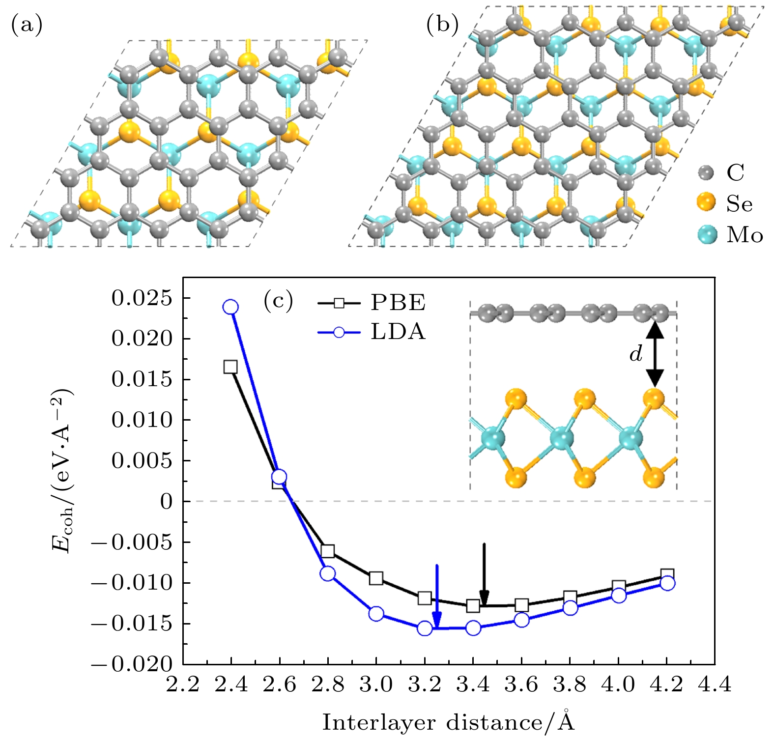
图 1 (a) 石墨烯4 × 4超胞和二硒化钼3 × 3超胞组成的异质结俯视图; (b) 石墨烯5 × 5超胞和二硒化钼4 × 4超胞组成的异质结俯视图; (c) PBE和LDA两种方法下层间距与石墨烯/二硒化钼异质结结合能的关系. 两个箭头表示两种方法下最低能量时的层间距
Figure 1. (a) Top views of heterostructure composed of 4 × 4 lateral periodicity of graphene and 3 × 3 lateral periodicity of MoSe2 monolayer; (b) top views of heterostructure composed of 5 × 5 lateral periodicity of graphene and 4 × 4 lateral periodicity of MoSe2 monolayer; (c) dependence of Ecoh in graphene/MoSe2 heterostructure on the interlayer distance under LDA and PBE methods. The two arrows indicate the d with the lowest Ecoh for LDA and PBE methods.
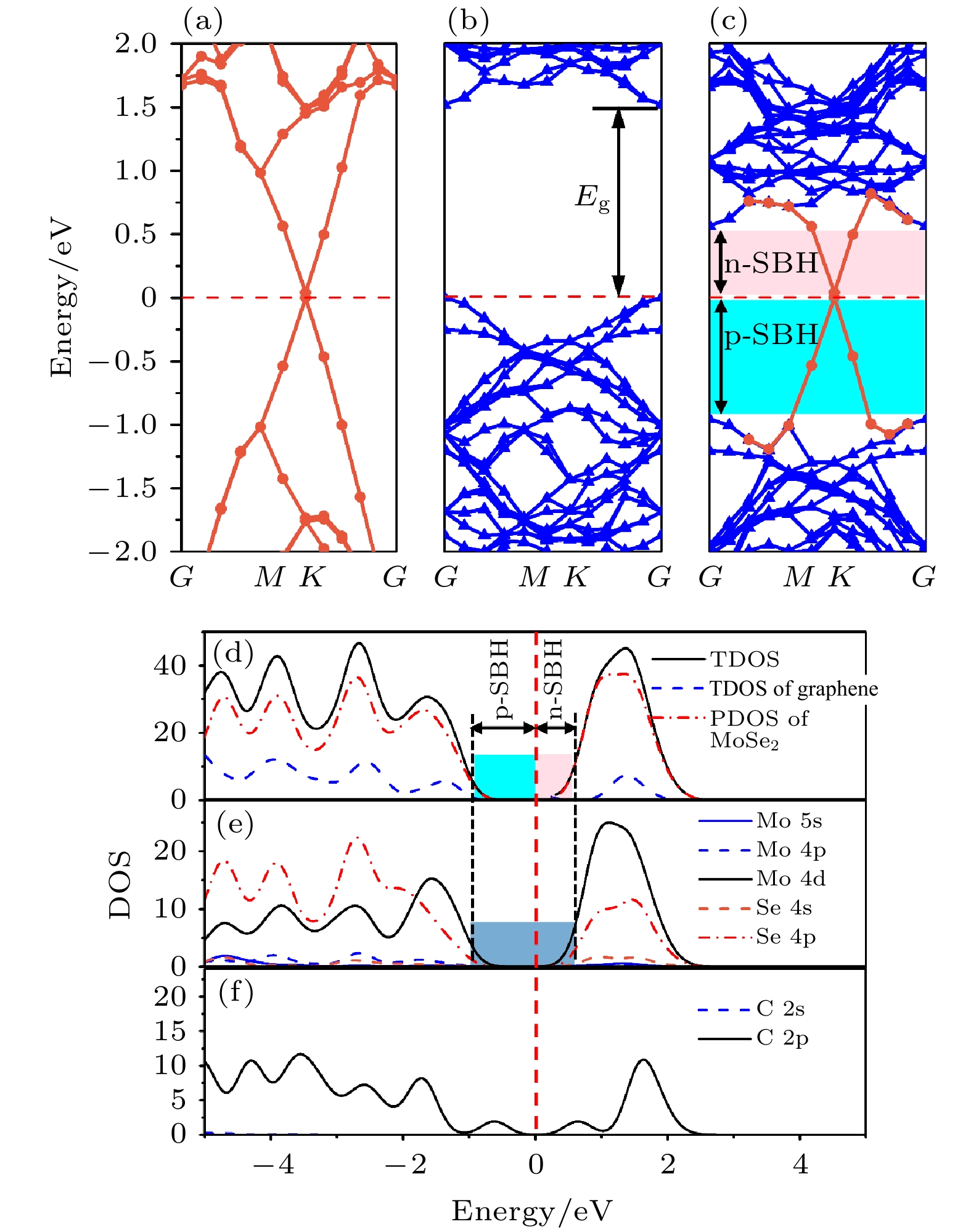
图 2 能带结构图 (a) 石墨烯; (b) 单层二硒化钼; (c) 石墨烯/二硒化钼异质结. (d) 石墨烯/二硒化钼异质结的总态密度和分态密度; (e) 异质结中二硒化钼的分态密度; (f) 异质结中石墨烯的分态密度. 费米能级设置为零, 用红色虚线表示
Figure 2. Band structures of (a) graphene; (b) MoSe2 monolayer; (c) graphene/MoSe2 heterostructure; (d) total density of states (DOS) and partial density of states (PDOS) of graphene/MoSe2 heterostructure; (e) PDOS of MoSe2 in the heterostructure; (f) PDOS of graphene in the heterostructure. The Fermi level is set to zero, denoted as a red dashed line.
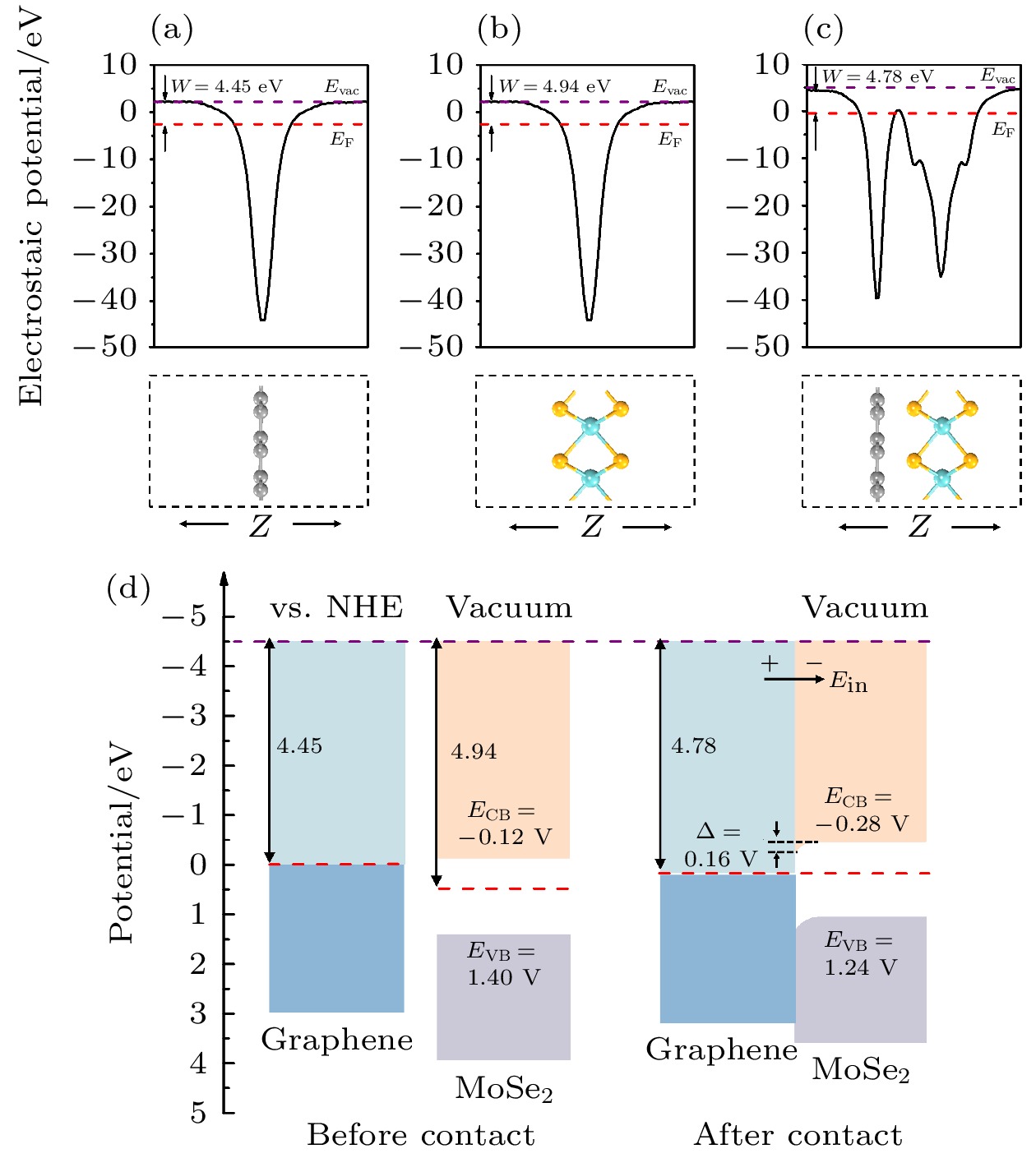
图 3 静电势 (a) 石墨烯; (b) 单层二硒化钼; (c) 石墨烯/二硒化钼异质结(红色和紫色虚线分别代表费米能级和真空能级); (d) 石墨烯和单层二硒化钼接触前和接触后的带边位置图
Figure 3. Electrostatic potentials of (a) graphene; (b) MoSe2 monolayer; (c) graphene/MoSe2 heterostructure(red and purple dashed lines represent the Fermi level and vacuum level, respectively); (d) energy level lineup diagrams for graphene and MoSe2 monolayer before and after contact.
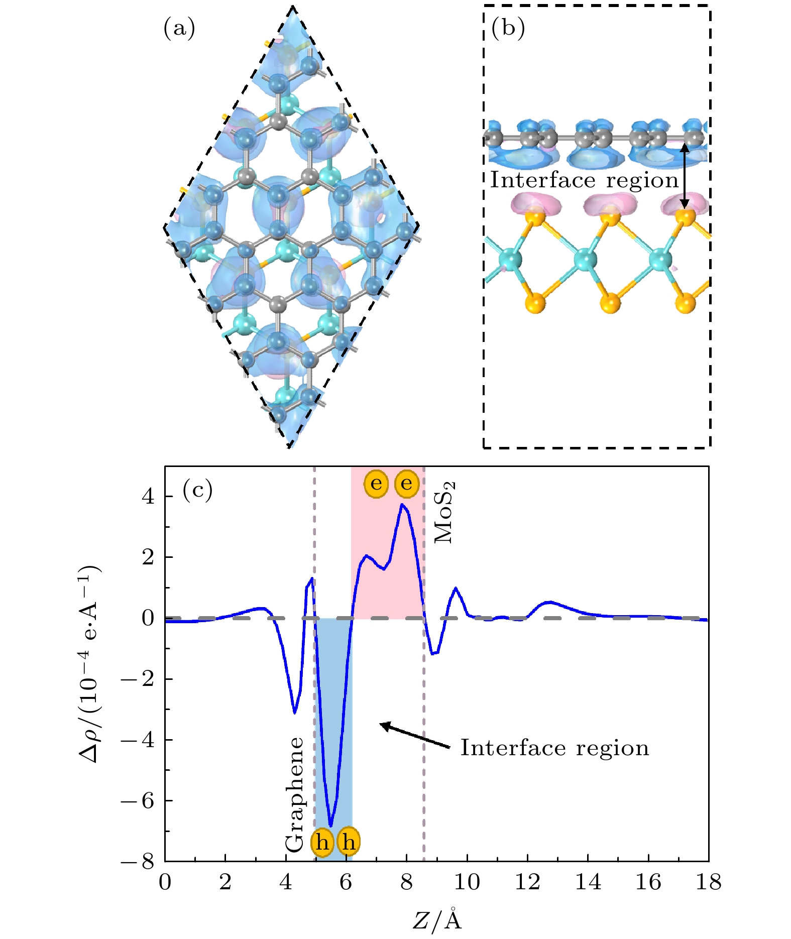
图 4 石墨烯/二硒化钼异质结的三维电荷密度差分 (a) 俯视图; (b) 侧视图; (c) 石墨烯/二硒化钼异质结的平面平均电荷密度差分
Figure 4. Three-dimensional charge density difference diagram of graphene/MoSe2 heterostructure: (a) Top view and (b) side view; (c) plane-averaged charge density difference of graphene/MoSe2 heterostructure.
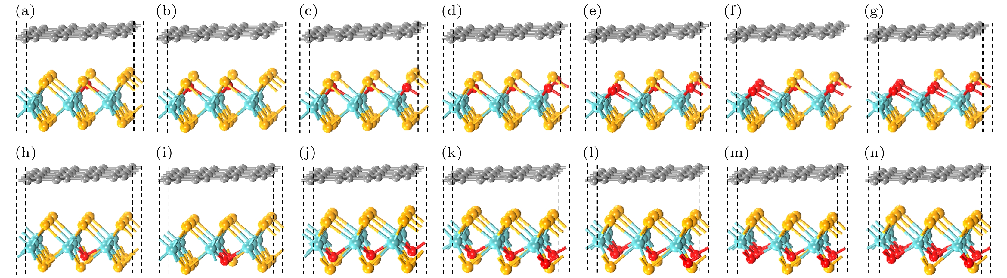
图 5 不同掺杂浓度的Gr/MoSe2(1–x)O2x异质结侧视图 (a)−(g) 对应界面内氧掺杂浓度分别为11%, 22%, 33%, 44%, 56%, 67%和78%; (h)−(n) 对应界面外氧掺杂浓度分别为11%, 22%, 33%, 44%, 56%, 67%和78%. 浅蓝色, 黄色, 灰色和红色的球分别表示钼, 硒, 碳和氧原子
Figure 5. Side views of the Gr/WSe2(1–x)O2x heterostructures with different concentrations of the oxygen dopant: (a)−(g) show the O doping on the inner interface are 11%, 22%, 33%, 44%, 56%, 67% and 78%, respectively. (h)−(n) represent the oxygen doping on the outer interface are 11%, 22%, 33%, 44%, 56%, 67% and 78%, respectively. The light blue, yellow, grey and red balls represent Mo, Se, C and O atoms, respectively.

图 6 不同氧掺杂浓度下Gr/MoSe2(1–x)O2x异质结的能带结构图 (a)−(g) 对应界面内氧掺杂浓度分别为11%, 22%, 33%, 44%, 56%, 67%和78%; (h)−(n) 对应界面外O掺杂浓度分别为11%, 22%, 33%, 44%, 56%, 67%和78%. 费米能级用红色虚线标记, 并设置为零
Figure 6. The band structures of the Gr/MoSe2(1–x)O2x heterostructure under asymmetric oxygen doping: (a)−(g) Show the oxygen doping on the inner interface are 11%, 22%, 33%, 44%, 56%, 67% and 78%, respectively; (h)−(n) represent the oxygen doping on the outer interface are 11%, 22%, 33%, 44%, 56%, 67% and 78%, respectively. The Fermi level is marked with a dashed red line and set to zero.

图 7 不同氧掺杂浓度下 (a) Gr/MoSe2(1–x)O2x异质结的肖特基势垒高度; (b) Gr/MoSe2(1–x)O2x异质结的功函数; (c) Gr/MoSe2(1–x)O2x异质结沿着Z方向氧掺杂在内表面和外表面的平面平均电荷密度差分图
Figure 7. Dependence of (a) the SBH and (b) work function in Gr/MoSe2(1–x)O2x heterostructure on the oxygen doping concentration; (c) calculated planar electron density differences of the Gr/MoSe2(1–x)O2x heterostructure along the Z direction in different oxygen doping concentrations inside and outside the interface.
表 1 不同氧原子掺杂浓度的Gr/MoSe2(1–x)O2x异质结失配率
Table 1. Mismatch ratio of Gr/MoS2(1–x)O2x heterosstructure with different oxygen doping concentration
氧原子掺杂浓度/% 晶格常数/Å (a = b) 失配率/% MoSe2(1–x)O2x Graphene 0 9.846 9.838 0.08 11 9.721 9.838 1.19 22 9.681 9.838 1.60 33 9.552 9.838 2.91 44 9.478 9.838 3.65 56 9.424 9.838 4.21 67 9.359 9.838 4.87 78 9.404 9.838 4.41 89 9.342 9.838 5.04 100 9.267 9.838 5.80  DownLoad: CSV
-
[1] Geim A K 2009 Science 324 1530
Google Scholar
[2] Novoselov K S, Jiang Z, Zhang Y, et al. 2007 Science 315 1379
Google Scholar
[3] Tonndorf P, Schmidt R, Böttger P, et al. 2013 Opt. express 21 4908
Google Scholar
[4] Rathi S, Lee I, Lim D, Wang J, Ochiai Y, Aoki N, Watanabe K, Taniguchi T, Lee G H, Yu Y J, Kim P, Kim G H 2015 Nano Lett. 15 5017
Google Scholar
[5] Ross J S, Wu S, Yu H, Ghimire N J, Jones A M, Aivazian G, Yan J, Mandrus D G, Xiao D, Yao W, Xu X 2013 Nat. Commun. 4 1474
Google Scholar
[6] Tongay S, Zhou J, Ataca C, Lo K, Matthews T S, Li J, Grossman J C, Wu J 2012 Nano Lett. 12 5576
Google Scholar
[7] Larentis S, Fallahazad B, Tutuc E 2012 Appl. Phys. Lett. 101 223104
Google Scholar
[8] Liu Y, Guo J, Zhu E, Liao L, Lee S J, Ding M, Shakir I, Gambin V, Huang Y, Duan X 2018 Nature 557 696
Google Scholar
[9] Bardeen J 1947 Phys. Rev. 71 717
Google Scholar
[10] Miedema A R, Chatel P F, Boer F R 1980 Physica 100 1
Google Scholar
[11] Çakır D, Sevik C, Peeters F 2014 J. Mater. Chem. C 2 9842
Google Scholar
[12] Hong X, Kim J, Shi S F, Zhang Y, Jin C, Sun Y, Tongay S, Wu J, Zhang Y, Wang F 2014 Nat. Nanotechnol. 9 682
Google Scholar
[13] Vu T V, Hieu N V, Phuc H V, Hieu N N, Bui H D, Idrees M, Amin B, Nguyen C V 2020 Appl. Surf. Sci. 507 145036
Google Scholar
[14] 郭丽娟, 胡吉松, 马新国, 项炬 2019 物理学报 68 097101
Google Scholar
Guo L J, Hu J S, Ma X G, Xiang J 2019 Acta Phys. Sin. 68 097101
Google Scholar
[15] Sata Y, Moriya R, Morikawa S, Yabuki N, Masubuchi S, Machida T 2015 Appl. Phys. Lett. 107 023109
Google Scholar
[16] Sun Z, Chu H, Li Y, Zhao S, Li G, Li D 2019 Mater. Design 183 108129
Google Scholar
[17] Hu J, Duan W, He H, Lv H, Huang C, Ma X 2019 J. Mater. Chem. C 7 7798
Google Scholar
[18] Weng J, Gao S P 2018 Phys. Chem. Chem. Phys. 20 26453
Google Scholar
[19] Perdew J, Burke K, Ernzerhof M 1996 Phys. Rev. Lett. 77 3865
Google Scholar
[20] Tkatchenko A, Scheffler M 2009 Phys. Rev. Lett. 102 073005
Google Scholar
[21] Chan K, Neaton J, Cohen M 2008 Phys. Rev. B 77 235430
Google Scholar
[22] Saha P, Ghosh B, Mazumder A, Mukherjee G D 2020 Mater. Res. Express 7 025902
Google Scholar
[23] Zhang R, Hao G, Ye X, Gao S, Li H 2020 Phys. Chem. Chem. Phys. 22 23699
Google Scholar
[24] Hieu N N, Phuc H V, Ilyasov V V, Chien N D, Poklonski N A, Van Hieu N, Nguyen C V 2017 J. Appl. Phys. 122 104301
Google Scholar
[25] Hu J, Ji G, Ma X, He H, Huang C 2018 Appl. Surf. Sci. 440 35
Google Scholar
[26] Zhang R, Hao G, Li H, Ye X, Gao S, Yuan X, Liu C 2020 J. Phys. Chem. Solids 143 109466
Google Scholar
[27] Peng Q, Wang Z, Sa B, Wu B, Sun Z 2016 Sci. Rep-UK 6 31994
Google Scholar
[28] Ugeda M, Bradley A, Shi S F, Da Jornada F, Zhang Y, Qiu D, Mo S K, Hussain Z, Shen Z X, Wang F, Louie S, Crommie M 2014 Nat. Mater. 13 1091
Google Scholar
[29] 危阳, 马新国, 祝林, 贺华, 黄楚云 2017 物理学报 66 087101
Google Scholar
Wei Y, Ma X G, Zhu L, He H, Huang C Y 2017 Acta Phys. Sin. 66 087101
Google Scholar
[30] Bjorkman T, Gulans A, Krasheninnikov A V, Nieminen R M 2012 Phys. Rev. Lett. 108 235502
Google Scholar
[31] Liu B, Wu L, Zhao Y, Wang L, Cai M 2016 RSC Adv. 6 60271
Google Scholar
[32] Ebnonnasir A, Narayanan B, Kodambaka S, Ciobanu C V 2014 Appl. Phys. Lett. 105 031603
Google Scholar
[33] Xu P, Tang Q, Zhou Z 2013 Nanotechnology 24 305401
Google Scholar
[34] Du A, Sanvito S, Li Z, Wang D, Jiao Y, Liao T, Sun Q, Ng Y H, Zhu Z, Amal R 2012 J. Am. Chem. Soc. 134 4393
Google Scholar
[35] Zhao Y, Lee H J, Choi W, Fei W, Lee C J 2017 RSC Adv. 7 27969
Google Scholar
[36] Zhang R, Hao G, Ye X, Zhang W, Li H 2021 J. Appl. Phys. 129 174302
Google Scholar

 DownLoad:
Catalog
Metrics
- Abstract views: 4899
- PDF Downloads: 148
- Cited By: 0
