


-
Reducing the Schottky barrier at the metal-semiconductor interface and achieving Ohmic contacts are very important for developing high-performance Schottky field-effect devices. Based on the fact that GaN and 1T-VSe2 monolayers have been successfully prepared experimentally, we theoretically construct a GaN/1T-VSe2 heterojunction model and investigate its stability, Schottky barrier property and its modulation effects by using first-principle method. The calculated formation energy and the molecular dynamics simulations show that the constructed heterojunction is very stable, meaning that it can be realized experimentally. The intrinsic heterojunction holds a p-type Schottky contact and always keeps the same p-type Schottky contact when tensile or compressive strain is applied. But when the external electric field is applied, the situation is different. For example, a higher forward electric field can cause the heterojunction to change from a Schottky contact into an Ohmic contact, and a higher reverse electric field can lead to a variation from a p-type Schottky contact to an n-type Schottky contact. In particular, by implementing chemical doping, the transition from Schottky contact to Ohmic contact can be achieved more easily for the heterojunction. For example, the introduction of B atom enables the GaN/1T-VSe2 heterojunction to realize a typical Ohmic contact, while for C and F atom doping, the GaN/1T-VSe2 heterojunction can achieve a quasi-Ohmic contact. These studies provide a theoretical reference for the practical application of the suggested heterojunction, and are of very important in designing novel high-performance nano-scale electronic devices.
-
Keywords:
- van der Waals heterojunction /
- Schottky barrier /
- Ohmic contact /
- physical regulation /
- chemical doping
[1] Shokri A, Esrafilian M, Salami N 2020 Physica E 119 113908
 Google Scholar
[2] Althib H 2021 Results Phys. 22 103943
Google Scholar
[3] Novoselov K S, Geim A K, Morozov S V, Jiang D, Zhang Y, Dubonos S V, Grigorieva I V, Firsov A A 2004 Science 306 666
Google Scholar
[4] Novoselov K S, Geim A K, Morozov S V, Jiang D, Katsnelson M I, Grigorieva I V, Dubonos S V, Firsov A A 2005 Nature 438 197
Google Scholar
[5] Dai X Y, Mitchell I, Kim S, An H, Ding F 2022 Carbon 199 233
Google Scholar
[6] Shu Y, He K J, Xiong R, Cui Z, Yang X H, Xu C, Zheng J J, Wen C L, Wu B, Sa B S 2022 Appl. Surf. Sci. 604 154540
Google Scholar
[7] Galashev A Y, Vorob’ev A S 2022 Physica E 138 115120
Google Scholar
[8] Karim H, Shahnaz, Batool M, Yaqub M, Saleem M, Gilani M A, Tabassum S 2022 Appl. Surf. Sci. 596 153618
Google Scholar
[9] Zhuo Q Z, Liu X J, OU J L, Fu Z T, Xu X Y 2022 Appl. Surf. Sci. 598 153719
Google Scholar
[10] Bi S H, Bi P, Xue M Z 2021 Comp. Mater. Sci. 197 110603
Google Scholar
[11] Xie M Q, Li Y, Liu X H, Li X A 2022 Appl. Surf. Sci. 591 153198
Google Scholar
[12] Wang Q H, Kalantar-Zadeh K, Kis A, Coleman J N, Strano M S 2012 Nat. Nanotechnol. 7 699
Google Scholar
[13] Butler S Z, Hollen S M, Cao L, et al. 2013 ACS Nano 7 2898
Google Scholar
[14] Anasori B, Lukatskaya M R, Gogotsi Y 2017 Nat. Rev. Mater. 2 16098
Google Scholar
[15] Naguib M, Kurtoglu M, Presser V, Lu J, Niu J, Min H, Hultman L, Gogotsi Y, Barsoum M W 2011 Adv. Mater. 23 4248
Google Scholar
[16] Song J G, Park J, Lee W, Choi T, Jung H, Lee C W, Hwang S H, Myoung J M, Jung J H, Kim S H, Lansalot-Matras C, Kim H 2013 ACS Nano 7 11333
Google Scholar
[17] Chang H Y, Yogeesh M N, Ghosh R, Rai A, Sanne A, Yang S, Lu N, Banerjee S K, Akinwande D 2016 Adv. Mater. 28 1818
Google Scholar
[18] Choi W B, Choudhary N, Han G H, Park J, Akinwande D, Lee Y H 2017 Mater. Today 20 116
Google Scholar
[19] Kim C, Moon I, Lee D, Choi M S, Ahmed F, Nam S, Cho Y, Shin H J, Park S, Yoo W J 2017 ACS Nano 11 1588
Google Scholar
[20] Song N H, Ling H, Wang Y S, Zhang L Y, Yang Y Y, Jia Y 2019 J. Solid State Chem. 269 513
Google Scholar
[21] Allain A, Kang J H, Banerjee K, Kis A 2015 Nat. Mater. 14 1195
Google Scholar
[22] Tung R T 2014 Appl. Phys. Rev. 1 54
Google Scholar
[23] Popov I, Seifert G, Tomanek D 2012 Phys. Rev. Lett. 108 156802
Google Scholar
[24] Chung K, Lee C, Yi G 2010 Science 330 655
Google Scholar
[25] Kobayashi Y, Kumakura K, Akasaka T, Makimoto T 2012 Nature 484 223
Google Scholar
[26] Freeman C L, Claeyssens F, Allan N L, Harding J H 2006 Phys. Rev. Lett. 96 066102
Google Scholar
[27] Ahin H, Cahangirov S, Topsakal M, Bekaroglu E, Ciraci S 2009 Phys. Rev. B 80 155453
Google Scholar
[28] Al Balushi Z Y, Wang K, Ghosh R K, Vilá R A, Eichfeld S M, Caldwell J D, Qin X Y, Lin Y C, DeSario P A, Stone G, Subramanian S, Paul D F, Wallace R M, Datta S, Redwing J M, Robinson J A 2016 Nat. Mater. 15 1166
Google Scholar
[29] Shen P F, Li E L, Zhang L, Zhao H Y, Cui Z, Ma D M 2021 Superlattice. Microst. 156 106930
Google Scholar
[30] Song J, Ding Z, Liu X F, Huang Z C, Li J W, Wei J M, Luo Z J, Wang J H, Guo X 2021 Comp. Mater. Sci. 197 110644
Google Scholar
[31] González-Ariza R, Martínez-Castro O, Moreno-Armenta M G, Gonzalez-Garcia A, Lopez-Perez W, Gonzalez-Hernandez R 2019 Physica B 569 57
Google Scholar
[32] Zhao Q, Xiong Z H, Qin Z Z, Chen L L, Wu N, Li X X 2016 J. Phys. Chem. Solids 91 1
Google Scholar
[33] Cui Z, Wang X, Li E L, Ding Y C, Sun C L, Sun M L 2018 Nanoscale Res. Lett. 13 207
Google Scholar
[34] Bonilla M, Kolekar S, Ma Y J, Diaz H C, Kalappattil V, Das R, Eggers T, Gutierrez H R, Phan M H, Batzill M 2018 Nat. Nanotechnol. 13 289
Google Scholar
[35] Chen P, Pai W W, Chan Y H, Madhavan V, Chou M Y, Mo S K, Fedorov A V, Chiang T C 2018 Phys. Rev. Lett. 121 196402
Google Scholar
[36] FengJ G, Biswas D, Rajan A, et al. 2018 Nano Lett. 18 4493
Google Scholar
[37] Zhang Z P, Gong Y, Zou X L, Liu P R, Yang P F, Shi J P, Zhao L Y, Zhang Q, Gu L, Zhang Y F 2019 ACS Nano 13 885
Google Scholar
[38] Hu H K, Zhang Z, Ouyang G 2020 Appl. Surf. Sci. 517 146168
Google Scholar
[39] Ma Y D, Dai Y, Guo M, Niu C W, Yua L, Huang B B 2011 Nanoscale 3 2301
Google Scholar
[40] Li Y H, Zhang Z H, Fan Z Q, Zhou R L 2020 J. Phys. Condens. Matter 32 015303
Google Scholar
[41] Zhao T, Fan Z Q, Zhang Z H, Zhou R L 2019 J. Phys. D Appl. Phys. 52 475301
Google Scholar
[42] Hu R, Li Y H, Zhang Z H, Fan Z Q, Sun L 2019 J. Mater. Chem. C 7 7745
Google Scholar
[43] 张仑, 陈红丽, 义钰, 张振华 2022 物理学报 71 177304
Google Scholar
Zhang L, Chen H L, Yi Y, Zhang Z H 2022 Acta Phys. Sin. 71 177304
Google Scholar
[44] Hu J K, Zhang Z H, Fan Z Q, Zhou R L 2019 Nanotechnology 30 485703
Google Scholar
[45] Si J G, Lu W J, Wu H Y, Lü H Y, Liang X, Li Q J, Sun Y P 2020 Phys. Rev. B 101 235405
Google Scholar
[46] Ma Y D, Dai Y, Guo M, Niu C W, Zhu Y T, Huang B B 2012 ACS Nano 6 1695
Google Scholar
[47] Grimme S 2006 J. Comput. Chem. 27 1787
Google Scholar
[48] Meng X S, Liu H L, Lin L K, Cheng Y B, Hou X, Zhao S Y, Lu H M, Meng X K 2021 Appl. Surf. Sci. 539 148302
Google Scholar
[49] Xia C X, Peng Y T, Wei S Y, Jia Y 2013 Acta Mater. 61 7720
Google Scholar
[50] Fu H R, Yan B H, Wu S C, Felser C, Chang C R 2016 New J. Phys. 18 113038
Google Scholar
[51] Yadava C S, Rastogi A K 2010 Solid State Commun. 150 648
Google Scholar
[52] Dai J Q, Yuan J, Ke C, Wei Z C 2021 Appl. Surf. Sci. 547 149206
Google Scholar
[53] Pham K, Nguyen C, Nguyen C, Cuong P, Hieu N 2021 New. J. Chem. 45 5509
Google Scholar
[54] Cui Z, Ren K, Zhao Y M, Wang X, Shu H B, Yu J, Tang W C, Sun M L 2019 Appl. Surf. Sci. 492 513
Google Scholar
[55] Vu T V, Hieu N V, Phuc H V, Hieu N N, Bui H D, Idrees M, Amin B, Nguyen C V 2020 Appl. Surf. Sci. 507 145036
Google Scholar
[56] Liu Y H, Li H, Liu F B, Sun S, Zhou G, Qing T, Zhang S H, Lu J 2022 Solid State Commun. 348 114770
Google Scholar
[57] Liu Y, Zhang W D, Lü B H, Ge Y, Zhang R G, Wang B J, Chen Z H, Zhang Q, Sang S B 2022 Surf. Interfaces 30 101823
Google Scholar
[58] 梁前, 钱国林, 罗祥燕, 梁永超, 谢泉 2022 物理学报 71 217301
Google Scholar
Liang Q, Qian G L, Luo X Y, Liang Y C, Xie Q 2022 Acta Phys. Sin. 71 217301
Google Scholar
[59] 张芳, 贾利群, 孙现亭, 戴宪起, 黄奇祥, 李伟 2020 物理学报 69 157302
Google Scholar
Zhang F, Jia L Q, Sun X T, Dai X Q, Huang Q X, Li W 2020 Acta Phys. Sin. 69 157302
Google Scholar
[60] Pérez-Tomás A, Fontserè A 2011 Solid State Electron. 56 201
Google Scholar
[61] Hu J S, Duan W Y, He H, Lü H, Huang C Y, Ma X G 2019 J. Mater. Chem. C 7 7798
Google Scholar
[62] 郝国强, 张瑞, 张文静, 陈娜, 叶晓军, 李红波 2022 物理学报 71 017104
Google Scholar
Hao G Q, Zhang R, Zhang W J, Chen N, Ye X J, Li H B 2022 Acta Phys. Sin. 71 017104
Google Scholar
[63] 汤家鑫, 范志强, 邓小清, 张振华 2022 物理学报 71 116101
Google Scholar
Tang J X, Fan Z Q, Deng X Q, Zhang Z H 2022 Acta Phys. Sin. 71 116101
Google Scholar
-

图 1 (a) GaN单层原子结构正视图和侧视图; (b) GaN单层能带结构和DOS; (c) 1T-VSe2单层原子结构正视图和侧视图; (d) 1T-VSe2单层能带结构, 其中黑色实线和虚线分别表示电子上旋和下旋能带结构
Figure 1. (a) Top and side views of GaN monolayer atomic structure; (b) band structure and DOS of GaN monolayer; (c) top and side views of 1T-VSe2 monolayer atomic structure; (d) band structure of 1T-VSe2 monolayer, in which the black solid line and dotted line represent the electronic α-spin and β-spin band structure, respectively.

图 2 GaN与1T-VSe2单层形成异质结时不同堆叠方式, GaN层的N原子分别对齐1T-VSe2层的(a) V原子, (b)上层Se原子, (c)下层Se原子, (d) V-Se键中间, 以及(e)空位, 并记为S1—S5. (f) 5种堆叠方式的最低能量的相对值ΔE
Figure 2. Different stacking configurations for GaN and 1T-VSe2 monolayers integrated to form heterojunctions. The N atom in top GaN layer is just aligned with the (a) V atom, (b) upper Se atoms, (c) lower Se atom, (d) middle of V—Se bond, and (e) hollow site in bottom 1T-VSe2 layer, which are marked as S1—S5, respectively. (f) Relative value of the lowest energy ΔE, for five stacking configurations.
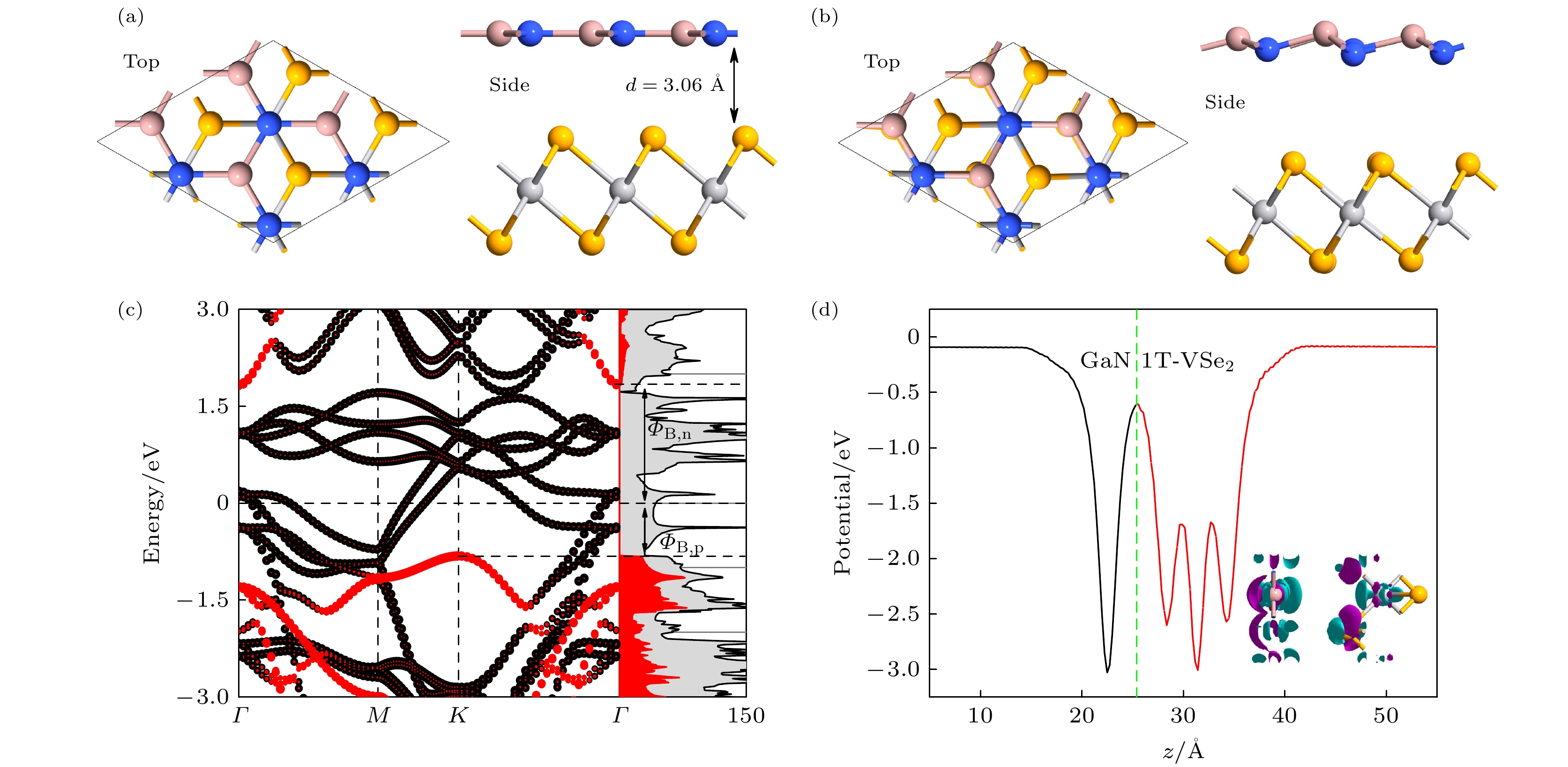
图 3 (a)本征异质结S1的正视图和侧视图; (b)进行淬火处理后异质结S1的正视图和侧视图; (c)异质结S1的能带结构以及DOS图, 红色和黑色分别表示GaN和1T-VSe2单层对能带的贡献, 灰色部分表示总DOS, 红色部分表示GaN的PDOS; (d) 异质结S1沿垂直方向的平均静电势以及空间电荷差密度, 其中青色表示失去电子, 紫色表示得到电子, 等值面为0.001 e·Å–3
Figure 3. (a) Top and side views for intrinsic heterojunction S1; (b) top and side views for heterojunction S1 after quenching treatment; (c) band structure and DOS of the heterojunction S1, red and black lines denote the respective contribution of GaN and 1T-VSe2 monolayers to the energy band structure, the gray part indicates the total density of states, and the red part indicates the PDOS of GaN; (d) the average electrostatic potential and space charge density difference in the vertical direction of heterojunction S1, where cyan represents the loss of electrons, and purple represents the gain of electrons, the isosurface is set to 0.001 e·Å–3.

图 4 垂直应变效应 (a)异质结S1施加应变示意图; (b)异质结的肖特基势垒高度 ΦB,n, ΦB,p和GaN单层的带隙Eg随层间距的变化, 绿色竖直虚线表示本征异质结层间距
Figure 4. Vertical strain effects: (a) Schematic diagram of applied strain for heterojunction S1; (b) Schottky barrier heights ΦB,n and ΦB,p, and the band gap Eg for GaN monolayers versus layer spacing, where the green vertical dotted line represents the layer spacing for intrinsic heterostructure .

图 5 异质结S1的能带结构随层间距的变化细节, 其中黑色表示1T-VSe2层的贡献, 橙色表示GaN层的贡献, 在费米能级附近的上下两个方框分别表示ΦB,n和ΦB,p
Figure 5. Detailed variation of energy band structure for heterojunction S1 with the layer spacing, where black represents the contribution of 1T-VSe2 layer, orange denotes the contribution of GaN layer, and the upper and lower two boxes around the Fermi level indicate ΦB,n and ΦB,p, respectively.

图 6 外加电场效应 (a)异质结S1施加外电场作用示意图; (b)异质结的肖特基势垒高度 ΦB,n, ΦB,p和GaN单层的带隙Eg随电场的变化
Figure 6. External electric field effects: (a) Schematic diagram of applying external electric field for heterojunction S1; (b) Schottky barrier height ΦB,n and ΦB,p, and the band gap Eg of GaN monolayer versus external electric field.

图 7 异质结S1的能带结构随外电场变化情况, 其中黑色表示1T-VSe2层的贡献, 橙色表示GaN层的贡献, 上下两个方框分别表示ΦB,n和ΦB,p
Figure 7. Energy band structure of heterojunction S1 changes with the external electric field in details, where black represents the contribution of 1T-VSe2 layer, orange denotes the contribution of GaN layer, and the upper and lower two boxes around the Fermi level indicate ΦB,n and ΦB,p, respectively.
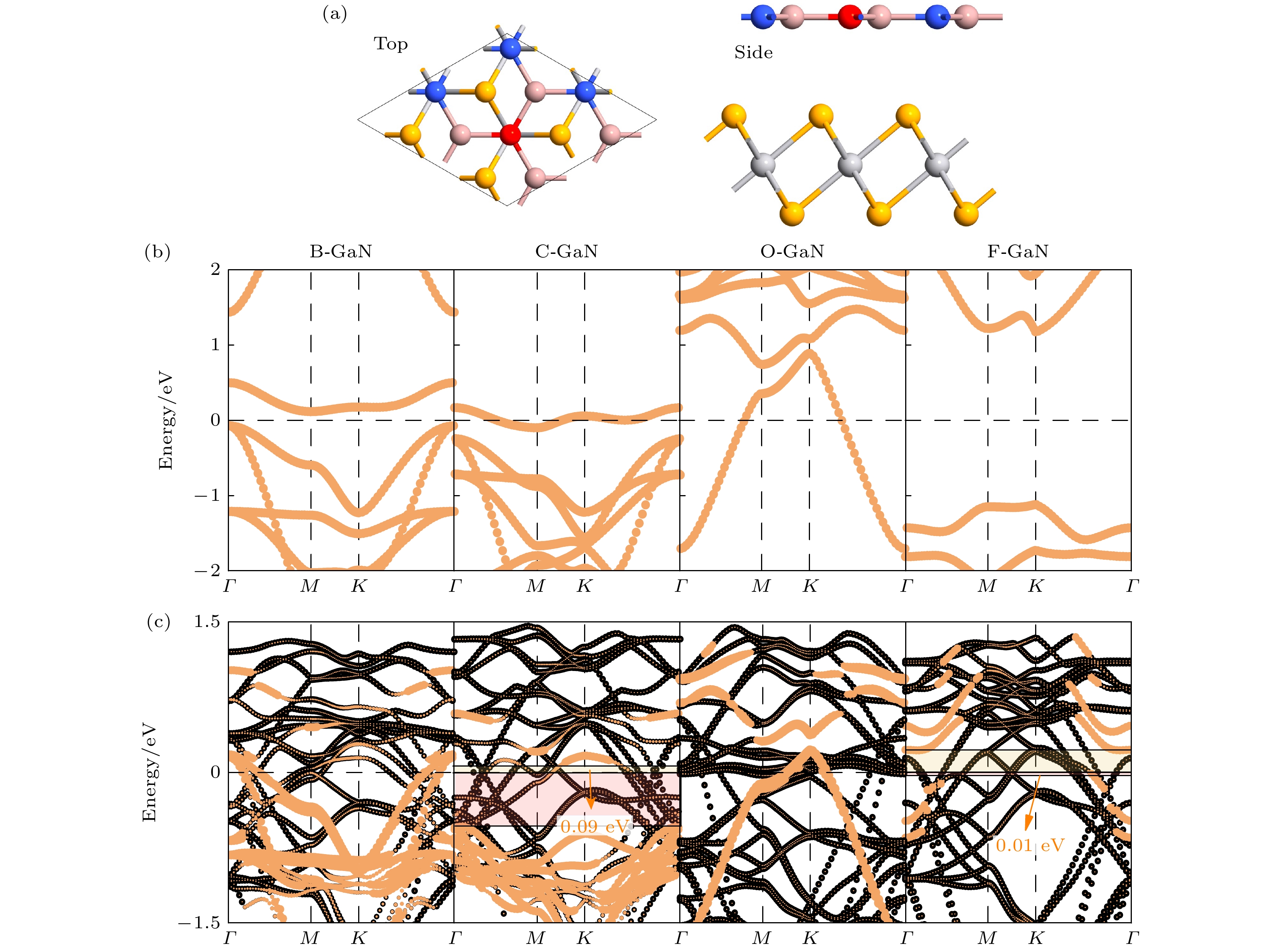
图 8 化学掺杂效应 (a) X-GaN/1T-VSe2异质结的原子结构正视图和侧视图; (b) X-GaN的能带结构; (c) X-GaN /1T-VSe2异质结的能带结构, 其中黑色表示1T-VSe2层的贡献, 橙色表示X-GaN层的贡献, 上下两个方框分别表示ΦB,n和ΦB,p
Figure 8. Chemical doping effects: (a) Top and side views of atomic structure for X-GaN/1T-VSe2 heterostructure; (b) energy band structure of X-GaN; (c) the energy band structure of the X-GaN/1T-VSe2 heterostructure, where black represents the contribution of 1T-VSe2 layer, orange denotes the contribution of GaN layer, and the upper and lower two boxes around the Fermi level indicate ΦB,n and ΦB,p, respectively.
-
[1] Shokri A, Esrafilian M, Salami N 2020 Physica E 119 113908
Google Scholar
[2] Althib H 2021 Results Phys. 22 103943
Google Scholar
[3] Novoselov K S, Geim A K, Morozov S V, Jiang D, Zhang Y, Dubonos S V, Grigorieva I V, Firsov A A 2004 Science 306 666
Google Scholar
[4] Novoselov K S, Geim A K, Morozov S V, Jiang D, Katsnelson M I, Grigorieva I V, Dubonos S V, Firsov A A 2005 Nature 438 197
Google Scholar
[5] Dai X Y, Mitchell I, Kim S, An H, Ding F 2022 Carbon 199 233
Google Scholar
[6] Shu Y, He K J, Xiong R, Cui Z, Yang X H, Xu C, Zheng J J, Wen C L, Wu B, Sa B S 2022 Appl. Surf. Sci. 604 154540
Google Scholar
[7] Galashev A Y, Vorob’ev A S 2022 Physica E 138 115120
Google Scholar
[8] Karim H, Shahnaz, Batool M, Yaqub M, Saleem M, Gilani M A, Tabassum S 2022 Appl. Surf. Sci. 596 153618
Google Scholar
[9] Zhuo Q Z, Liu X J, OU J L, Fu Z T, Xu X Y 2022 Appl. Surf. Sci. 598 153719
Google Scholar
[10] Bi S H, Bi P, Xue M Z 2021 Comp. Mater. Sci. 197 110603
Google Scholar
[11] Xie M Q, Li Y, Liu X H, Li X A 2022 Appl. Surf. Sci. 591 153198
Google Scholar
[12] Wang Q H, Kalantar-Zadeh K, Kis A, Coleman J N, Strano M S 2012 Nat. Nanotechnol. 7 699
Google Scholar
[13] Butler S Z, Hollen S M, Cao L, et al. 2013 ACS Nano 7 2898
Google Scholar
[14] Anasori B, Lukatskaya M R, Gogotsi Y 2017 Nat. Rev. Mater. 2 16098
Google Scholar
[15] Naguib M, Kurtoglu M, Presser V, Lu J, Niu J, Min H, Hultman L, Gogotsi Y, Barsoum M W 2011 Adv. Mater. 23 4248
Google Scholar
[16] Song J G, Park J, Lee W, Choi T, Jung H, Lee C W, Hwang S H, Myoung J M, Jung J H, Kim S H, Lansalot-Matras C, Kim H 2013 ACS Nano 7 11333
Google Scholar
[17] Chang H Y, Yogeesh M N, Ghosh R, Rai A, Sanne A, Yang S, Lu N, Banerjee S K, Akinwande D 2016 Adv. Mater. 28 1818
Google Scholar
[18] Choi W B, Choudhary N, Han G H, Park J, Akinwande D, Lee Y H 2017 Mater. Today 20 116
Google Scholar
[19] Kim C, Moon I, Lee D, Choi M S, Ahmed F, Nam S, Cho Y, Shin H J, Park S, Yoo W J 2017 ACS Nano 11 1588
Google Scholar
[20] Song N H, Ling H, Wang Y S, Zhang L Y, Yang Y Y, Jia Y 2019 J. Solid State Chem. 269 513
Google Scholar
[21] Allain A, Kang J H, Banerjee K, Kis A 2015 Nat. Mater. 14 1195
Google Scholar
[22] Tung R T 2014 Appl. Phys. Rev. 1 54
Google Scholar
[23] Popov I, Seifert G, Tomanek D 2012 Phys. Rev. Lett. 108 156802
Google Scholar
[24] Chung K, Lee C, Yi G 2010 Science 330 655
Google Scholar
[25] Kobayashi Y, Kumakura K, Akasaka T, Makimoto T 2012 Nature 484 223
Google Scholar
[26] Freeman C L, Claeyssens F, Allan N L, Harding J H 2006 Phys. Rev. Lett. 96 066102
Google Scholar
[27] Ahin H, Cahangirov S, Topsakal M, Bekaroglu E, Ciraci S 2009 Phys. Rev. B 80 155453
Google Scholar
[28] Al Balushi Z Y, Wang K, Ghosh R K, Vilá R A, Eichfeld S M, Caldwell J D, Qin X Y, Lin Y C, DeSario P A, Stone G, Subramanian S, Paul D F, Wallace R M, Datta S, Redwing J M, Robinson J A 2016 Nat. Mater. 15 1166
Google Scholar
[29] Shen P F, Li E L, Zhang L, Zhao H Y, Cui Z, Ma D M 2021 Superlattice. Microst. 156 106930
Google Scholar
[30] Song J, Ding Z, Liu X F, Huang Z C, Li J W, Wei J M, Luo Z J, Wang J H, Guo X 2021 Comp. Mater. Sci. 197 110644
Google Scholar
[31] González-Ariza R, Martínez-Castro O, Moreno-Armenta M G, Gonzalez-Garcia A, Lopez-Perez W, Gonzalez-Hernandez R 2019 Physica B 569 57
Google Scholar
[32] Zhao Q, Xiong Z H, Qin Z Z, Chen L L, Wu N, Li X X 2016 J. Phys. Chem. Solids 91 1
Google Scholar
[33] Cui Z, Wang X, Li E L, Ding Y C, Sun C L, Sun M L 2018 Nanoscale Res. Lett. 13 207
Google Scholar
[34] Bonilla M, Kolekar S, Ma Y J, Diaz H C, Kalappattil V, Das R, Eggers T, Gutierrez H R, Phan M H, Batzill M 2018 Nat. Nanotechnol. 13 289
Google Scholar
[35] Chen P, Pai W W, Chan Y H, Madhavan V, Chou M Y, Mo S K, Fedorov A V, Chiang T C 2018 Phys. Rev. Lett. 121 196402
Google Scholar
[36] FengJ G, Biswas D, Rajan A, et al. 2018 Nano Lett. 18 4493
Google Scholar
[37] Zhang Z P, Gong Y, Zou X L, Liu P R, Yang P F, Shi J P, Zhao L Y, Zhang Q, Gu L, Zhang Y F 2019 ACS Nano 13 885
Google Scholar
[38] Hu H K, Zhang Z, Ouyang G 2020 Appl. Surf. Sci. 517 146168
Google Scholar
[39] Ma Y D, Dai Y, Guo M, Niu C W, Yua L, Huang B B 2011 Nanoscale 3 2301
Google Scholar
[40] Li Y H, Zhang Z H, Fan Z Q, Zhou R L 2020 J. Phys. Condens. Matter 32 015303
Google Scholar
[41] Zhao T, Fan Z Q, Zhang Z H, Zhou R L 2019 J. Phys. D Appl. Phys. 52 475301
Google Scholar
[42] Hu R, Li Y H, Zhang Z H, Fan Z Q, Sun L 2019 J. Mater. Chem. C 7 7745
Google Scholar
[43] 张仑, 陈红丽, 义钰, 张振华 2022 物理学报 71 177304
Google Scholar
Zhang L, Chen H L, Yi Y, Zhang Z H 2022 Acta Phys. Sin. 71 177304
Google Scholar
[44] Hu J K, Zhang Z H, Fan Z Q, Zhou R L 2019 Nanotechnology 30 485703
Google Scholar
[45] Si J G, Lu W J, Wu H Y, Lü H Y, Liang X, Li Q J, Sun Y P 2020 Phys. Rev. B 101 235405
Google Scholar
[46] Ma Y D, Dai Y, Guo M, Niu C W, Zhu Y T, Huang B B 2012 ACS Nano 6 1695
Google Scholar
[47] Grimme S 2006 J. Comput. Chem. 27 1787
Google Scholar
[48] Meng X S, Liu H L, Lin L K, Cheng Y B, Hou X, Zhao S Y, Lu H M, Meng X K 2021 Appl. Surf. Sci. 539 148302
Google Scholar
[49] Xia C X, Peng Y T, Wei S Y, Jia Y 2013 Acta Mater. 61 7720
Google Scholar
[50] Fu H R, Yan B H, Wu S C, Felser C, Chang C R 2016 New J. Phys. 18 113038
Google Scholar
[51] Yadava C S, Rastogi A K 2010 Solid State Commun. 150 648
Google Scholar
[52] Dai J Q, Yuan J, Ke C, Wei Z C 2021 Appl. Surf. Sci. 547 149206
Google Scholar
[53] Pham K, Nguyen C, Nguyen C, Cuong P, Hieu N 2021 New. J. Chem. 45 5509
Google Scholar
[54] Cui Z, Ren K, Zhao Y M, Wang X, Shu H B, Yu J, Tang W C, Sun M L 2019 Appl. Surf. Sci. 492 513
Google Scholar
[55] Vu T V, Hieu N V, Phuc H V, Hieu N N, Bui H D, Idrees M, Amin B, Nguyen C V 2020 Appl. Surf. Sci. 507 145036
Google Scholar
[56] Liu Y H, Li H, Liu F B, Sun S, Zhou G, Qing T, Zhang S H, Lu J 2022 Solid State Commun. 348 114770
Google Scholar
[57] Liu Y, Zhang W D, Lü B H, Ge Y, Zhang R G, Wang B J, Chen Z H, Zhang Q, Sang S B 2022 Surf. Interfaces 30 101823
Google Scholar
[58] 梁前, 钱国林, 罗祥燕, 梁永超, 谢泉 2022 物理学报 71 217301
Google Scholar
Liang Q, Qian G L, Luo X Y, Liang Y C, Xie Q 2022 Acta Phys. Sin. 71 217301
Google Scholar
[59] 张芳, 贾利群, 孙现亭, 戴宪起, 黄奇祥, 李伟 2020 物理学报 69 157302
Google Scholar
Zhang F, Jia L Q, Sun X T, Dai X Q, Huang Q X, Li W 2020 Acta Phys. Sin. 69 157302
Google Scholar
[60] Pérez-Tomás A, Fontserè A 2011 Solid State Electron. 56 201
Google Scholar
[61] Hu J S, Duan W Y, He H, Lü H, Huang C Y, Ma X G 2019 J. Mater. Chem. C 7 7798
Google Scholar
[62] 郝国强, 张瑞, 张文静, 陈娜, 叶晓军, 李红波 2022 物理学报 71 017104
Google Scholar
Hao G Q, Zhang R, Zhang W J, Chen N, Ye X J, Li H B 2022 Acta Phys. Sin. 71 017104
Google Scholar
[63] 汤家鑫, 范志强, 邓小清, 张振华 2022 物理学报 71 116101
Google Scholar
Tang J X, Fan Z Q, Deng X Q, Zhang Z H 2022 Acta Phys. Sin. 71 116101
Google Scholar

 DownLoad:
Catalog
Metrics
- Abstract views: 1677
- PDF Downloads: 61
- Cited By: 0
