


-
Graphene-based van der Waals heterojunctions can not only modulate the electronic properties of graphene but also retain the superior properties of the original monolayer. In this paper, the structure, electrical contact types, electronic and optical properties of graphene/C3N van der Waals heterojunctions are systematically investigated based on first-principles calculations. We find that there is a p-type Schottky contact of only 0.039 eV in the graphene/C3N van der Waals heterojunctions in an equilibrium state. The external electric field can adjust the interface contact type, specifically, from p-type to n-type Schottky contact, or from p-type Schottky contact to Ohmic contact. The vertical strain not only opens a nonnegligible band gap of 360 meV on the Dirac cone of graphene in graphene/C3N van der Waals heterojunctions, but also modulates the band gap of C3N in the heterojunctions. Moreover, both the doping type and concentration of the carriers can be effectively tuned by the applied electric field and the vertical strain. The increase in carrier concentration is more pronounced by the applied electric field. Comparing with the pristine monolayer graphene and monolayer C3N, the optical response range and the light absorption rate of graphene /C3N van der Waals heterojunctions are enhanced. Main absorption peak in the spectrum reaches to 106 cm–1. These results not only provide valuable theoretical guidance for designing Schottky-based graphene/C3N van der Waals heterojunctions devices, but also further explore the potential applications of heterojunctions in optoelectronic nanodevices and field-effect transistor devices.
-
Keywords:
- van der Waals heterojunctions /
- Schottky contact /
- Ohmic contact /
- electrical contact
[1] Novoselov K S, Geim A K, Morozov S V, Jiang D E, Zhang Y, Dubonos S V, Grigorieva I V, Firsov A A 2004 Science 306 666
 Google Scholar
[2] Nandanapalli K R, Mudusu D, Lee S 2019 Carbon 152 954
Google Scholar
[3] Aditya D G, Abhay R S, Vilasrao J K 2017 Current Drug Targets. 18 724
Google Scholar
[4] Neto A C, Guinea F, Peres N M, Novoselov K S, Geim A K 2009 Rev. Mod. Phys. 81 109
Google Scholar
[5] Liu S X, Li Z J, Ge Y Q, Wang H D, Yue R, Jiang X T, Li J Q, Wen Q, Zhang H 2017 Photonics Res. 5 662
Google Scholar
[6] Mahmood J, Lee E K, Jung M, Shin D, Choi H J, Seo J M, Jung S M, Kim D, Li F, Lah M S, Park N, Shin H J, Oh J H, Baek J B 2016 Proc. Natl. Acad. Sci. 113 7414
Google Scholar
[7] Li X L, Wang X R, Zhang L, Lee S W, Dai H J 2008 Science 319 1229
Google Scholar
[8] Son J, Lee S, Kim S J, Park B C, Lee H K, Kim S, Kim J H, Hong B H, Hong J 2016 Nat. Commun. 7 13261
Google Scholar
[9] Fan X F, Shen Z X, Liu A Q, Kuo J L 2012 Nanoscale 4 2157
Google Scholar
[10] Shinde P P, Kumar V 2011 Phys. Rev. B 84 125401
Google Scholar
[11] Cui Z, Ren K, Zhao Y M, Wang X, Shu H B, Yu J, Tang W C, Sun M L 2019 Appl. Surf. Sci. 492 513
Google Scholar
[12] Chen D C, Lei X L, Wang Y N, Zhong S Y, Liu G, Xu B, Ouyang C Y 2019 Appl. Surf. Sci. 497 143809
Google Scholar
[13] Pierucci D, Henck H, Avila J, Balan A, Naylor C H, Patriarche G, Dappe Y J, Silly M G, Sirotti F, Johnson A C 2016 Nano. Lett. 16 4054
Google Scholar
[14] Chen H, Zhao J, Huang J, Liang Y 2019 Phys. Chem. Chem. Phys. 21 7447
Google Scholar
[15] Pham K D, Hieu N N, Phuc H V, Fedorov I A, Duque C A, Amin B, Nguyen C V 2018 Appl. Phys. Lett. 113 171605
Google Scholar
[16] Allain A, Kang J, Banerjee K, Kis A 2015 Nat. Mater. 14 1195
Google Scholar
[17] Mott N F 1939 MPS 171 27
[18] Tung R T 2014 Appl. Phys. Rev. 1 011304
Google Scholar
[19] Liu Y, Guo J, Zhu E B, Liao L, Lee S J, Ding M N, Shakir I, Gambin V, Huang Y, Duan X F 2018 Nature 557 696
Google Scholar
[20] Bardeen J 1947 Phys. Rev. 71 717
Google Scholar
[21] Hasegawa H, Sawada T 1983 Thin Solid Films 103 119
Google Scholar
[22] Amsalem P, Niederhausen J, Wilke A, Heimel G, Schlesinger R, Winkler S, Vollmer A, Rabe J, Koch N 2013 Phys. Rev. B 87 035440
Google Scholar
[23] Zhou X, Hu X Z, Zhou S S, Song H Y, Zhang Q, Pi L J, Li L, Li H Q, Lü J T, Zhai T Y 2018 Adv. Mater. 30 1703286
Google Scholar
[24] Guo J, Wang L Y, Yu Y W, Wang P Q, Huang Y, Duan X F 2019 Adv. Mater. 31 1902962
Google Scholar
[25] Zheng D Q, Zhao Z, Huang R, Nie J, Li L, Zhang Y 2017 Nano. Energy 32 448
Google Scholar
[26] Yang S W, Li W, Ye C C, Wang G, Tian H, Zhu C, He P, Ding G Q, Xie X M, Liu Y, Lifshitz Y, Lee S T, Kang Z H, Jiang M H 2017 Adv. Mater. 29 1605625
Google Scholar
[27] Kang D W, Zuo Z W, Zhang S, Wang Z W, Zhang L L 2020 Appl. Phys. Lett. 116 153103
Google Scholar
[28] Zhao J, Zeng H, Zhou X 2019 Carbon 145 1
Google Scholar
[29] Brandbyge M, Mozos J L, Ordejón J, Taylor J, Stokbro K 2002 Phys. Rev. B 65 165401
Google Scholar
[30] Deng Y X, Chen S Z, Zeng Y, Feng Y, Zhou W X, Tang L M, Chen K Q 2018 Org. Electron. 63 310
Google Scholar
[31] Liu H R, Gao R, Yang J E, Yang F, Wang T X, Zhang Z X, Liu X G, Jia H S, Xu B S, Ma H 2020 Appl. Surf. Sci. 525 146476
Google Scholar
[32] Yazyev O V, Louie S G 2010 Phys. Rev. B 81 195420
Google Scholar
[33] Zhang D B, Hu Y, Zhong H X, Yuan S J, Liu C 2019 Nanoscale 11 13800
Google Scholar
[34] Hu Q, Wu Q, Wang H, He J, Zhang G 2012 Phys. Status Solidi (b) 249 784
Google Scholar
[35] Gao X, Shen Y, Ma Y, Wu S, Zhou Z 2019 Comput. Mater Sci. 170 109200
Google Scholar
[36] Nguyen C V, Idrees M, Phuc H V, Hieu N N, Binh N T, Amin B, Vu T V 2020 Phys. Rev. B 101 235419
Google Scholar
[37] Xiong W X, Xia C X, Zhao X, Wang T X, Jia Y 2016 Carbon 109 737
Google Scholar
[38] Gao X, Shen Y Q, Ma Y Y, Wu S Y, Zhou Z X 2019 Carbon 146 337
Google Scholar
[39] Zhang W, Hao G, Zhang R, Xu J, Ye X, Li H 2021 Phys. Chem. Solids 157 110189
Google Scholar
[40] Zeng H, Chen R S, Yao G 2020 Adv. Electron. Mater. 6 1901024
Google Scholar
[41] Xu H, Wu J, Chen Y, Zhang H, Zhang J 2013 Chem. Asian J. 8 2446
Google Scholar
[42] Kim S M, Hsu A, Araujo P, Lee Y H, Palacios T S, Dresselhaus M, Idrobo J C, Kim K K, Kong J 2013 Nano Lett. 13 933
Google Scholar
[43] Liu H, Chen X, Deng L, Su X, Guo K, Zhu Z 2016 Electrochim. Acta 206 184
Google Scholar
[44] Hou C, Tai G A, Liu B, Wu Z H, Yin Y H 2021 Nano Res. 14 2337
Google Scholar
[45] Yin H F, Cao Y, Fan T L, Zhang M, Yao J C, Li P F, Chen S M, Liu X H 2021 Sci. Total Environ. 754 141926
Google Scholar
[46] Liu Y, Chen P, Chen Y, Lu H, Wang J, Yang Z, Lu Z, Li M, Fang L 2016 RSC Adv. 6 10802
Google Scholar
[47] Alcudia-Ramos M, Fuentez-Torres M, Ortiz-Chi F, Espinosa-González C, Hernández-Como N, García-Zaleta D, Kesarla M, Torres-Torres J, Collins-Martínez V, Godavarthi S 2020 Ceram. Int. 46 38
Google Scholar
[48] Mak K F, Shan J 2016 Nat. Photonics 10 216
Google Scholar
[49] Qi S M, Jiang J W, Wang X C, Mi W B 2021 Carbon 174 540
Google Scholar
[50] Phuc H V, Hieu N N, Hoi B D, Nguyen C V 2018 Phys. Chem. Chem. Phys. 20 17899
Google Scholar
[51] Zeng H, Zhao J, Cheng A Q, Zhang L, He Z, Chen R S 2018 Nanotechnology 29 075201
Google Scholar
[52] Mohanta M K, Sarkar A D 2021 Appl. Surf. Sci. 540 148389
Google Scholar
[53] Lee G H, Yu Y J, Cui X, Petrone N, Lee C H, Choi M S, Lee D Y, Lee C, Yoo W J, Watanabe K, Taniguchi T, Nuckolls C, Kim P, Hone J 2013 ACS Nano 7 9
[54] Vu T V, Hieu N V, Phuc H V, Hieu N N, Bui H, Idrees M, Amin B, Nguyen C V 2020 Appl. Surf. Sci. 507 145036
Google Scholar
[55] Yankowitz M, Watanabe K, Taniguchi T, San-Jose P, LeRoy B J 2016 Nat. Commun. 7 13168
Google Scholar
[56] Fülöp B, Márffy A, Tóvári E, Kedves M, Zihlmann S, Indolese D, Kovács-Krausz Z, Watanabe K, Taniguchi T, Schönenberger C, Kézsmárki I, Makk P, Csonka S 2021 J. Appl. Phys. 130 064303
Google Scholar
[57] Cho C, Wong J, Taqieddin A, Biswas S, Aluru N R, Nam S, Atwater H A 2021 Nano Lett. 21 3956
Google Scholar
[58] Tongay S, Fan W, Kang J, Park J, Koldemir U, Suh J, Narang D S, Liu K, Ji J, Li J, Sinclair R, Wu J 2014 Nano Lett. 14 3185
Google Scholar
[59] Fang H, Battaglia C, Carraro C, Nemsak S, Ozdol B, Kang J S, Bechtel H A, Desai S B, Kronast F, Unal A A, Conti C, Conlon C, Palsson G K, Martin M C, Minor A M, Fadley C S, Yablonovitch E, Maboudian R, Javey A 2014 Natl. Acad. Sci. 111 6198
Google Scholar
[60] Hu W, Li Z, Yang J 2013 Jpn. J. Appl. Phys. 139 154704
[61] Deng S, Li L, Rees P 2019 ACS Appl. Nano. Mater 2 3977
Google Scholar
[62] Gao X, Shen Y Q, Ma Y Y, Wu S Y, Zhou Z X 2019 Appl. Surf. Sci. 479 1098
Google Scholar
-

图 1 (a) Top堆叠模式的顶视图, 蓝色为N原子, 橙色为C原子; (b) Top堆叠模式的侧视图, d0是平衡层间距(3.15 Å); (c) 层间结合能作为层间距d的函数, 黄色(红色)背景对应于垂直压缩(拉伸)应变; (d) Gr/C3N vdWH平衡态下的声子谱; (e) 温度为300 K的分子动力学模拟, Gr/ C3N vdWH总能量在时长为10 ps内的变化, 插图为模拟结束时的结构
Figure 1. (a) Top view of the Top mode with N atoms in blue, C atoms in orange; (b) side view of the top mode configuration, d0 is the equilibrium interlayer spacing (3.15 Å); (c) interlayer binding energy as a function of the interlayer distance d, the yellow (red) background corresponds to the applied vertical compressive (stretch) strain; (d) phonon spectrum of Gr/C3N vdWH in equilibrium; (e) molecular dynamics simulation at a temperature of 300 K, the total energy of Gr/C3N vdWH varies over a time duration of 10 ps. The inset shows the structure at the end of the simulation.

图 2 (a) Gr/C3N vdWH平衡态下的投影能带, 黑色部分是Gr的能带, 红色部分是C3N的能带; (b) 平面平均电荷密度差, 橙色部分表示电子积累, 蓝色部分表示电子耗尽; (c) Gr/C3N vdWH在沿Z方向的平衡层间距的静电势. 黑色部分是Gr, 红色部分是C3N
Figure 2. (a) Projected energy band of Gr/C3N vdWH with equilibrium configuration. The black part corresponds to the energy band of Gr and the red part corresponds to the energy band of C3N; (b) the plane-average deformation charge density, the orange part indicates electron accumulation, the blue part indicates electron depletion; (c) electrostatic potential of Gr/C3N vdWH at the equilibrium interlayer spacing along the Z-direction, the black part corresponds to Gr and the red part corresponds to C3N.

图 3 (a) Gr/C3N vdWH中单层Gr和单层C3N的SBH和带隙宽度随外加电场强度变化曲线; (b) 不同强度正电场下异质结的能带结构; (c) 不同强度负电场下异质结的能带结构, 绿色(紫色)范围与
$ {\varPhi _{\text{n}}} $ ($ {\varPhi _{\text{p}}} $ )相对应Figure 3. (a) Trend of SBH and band gap of Gr and C3N in the Gr/C3N vdWH with the electric field; (b) the band structure of heterojunction at different positive electric fields; (c) the band structure of heterojunction at different negative electric fields, the green (purple) range corresponds to
$ {\varPhi _{\text{n}}} $ ($ {\varPhi _{\text{p}}} $ ).
图 4 (a) Gr/C3N vdWH中单层Gr和单层C3N的SBH和带隙随层间距(d)的变化曲线; (b) 异质结在压缩应变下的能带结构; (c) 拉伸应变下异质结的能带结构, 浅绿色范围对应于Gr被打开的带隙宽度
Figure 4. (a) Trend of SBH and band gap of Gr and C3N in the Gr/C3N vdWH with the interlayer distance(d); (b) the band structure of the heterojunction under compressive strains; (c) the band structure of the heterojunction under tensile strain, the light green range corresponds to the band gap width of Gr being opened.

图 5 (a) 不同层间距下的
$ \Delta {E_{\text{D}}} $ ; (b) 掺杂载流子浓度$ {N_{{\text{h/e}}}} $ 作为层间距的变化曲线; (c) 不同强度电场下的$ \Delta {E_{\text{D}}} $ ; (d) 掺杂载流子浓度$ {N_{{\text{h/e}}}} $ 随着外加电场的变化Figure 5. (a)
$ \Delta {E_{\text{D}}} $ at different interlayer distances; (b) doped carrier concentration$ {N_{{\text{h/e}}}} $ as a function of interlayer distance; (c)$ \Delta {E_{\text{D}}} $ at different electric fields; (d) doped carrier concentration$ {N_{{\text{h/e}}}} $ as a function of applied electric field.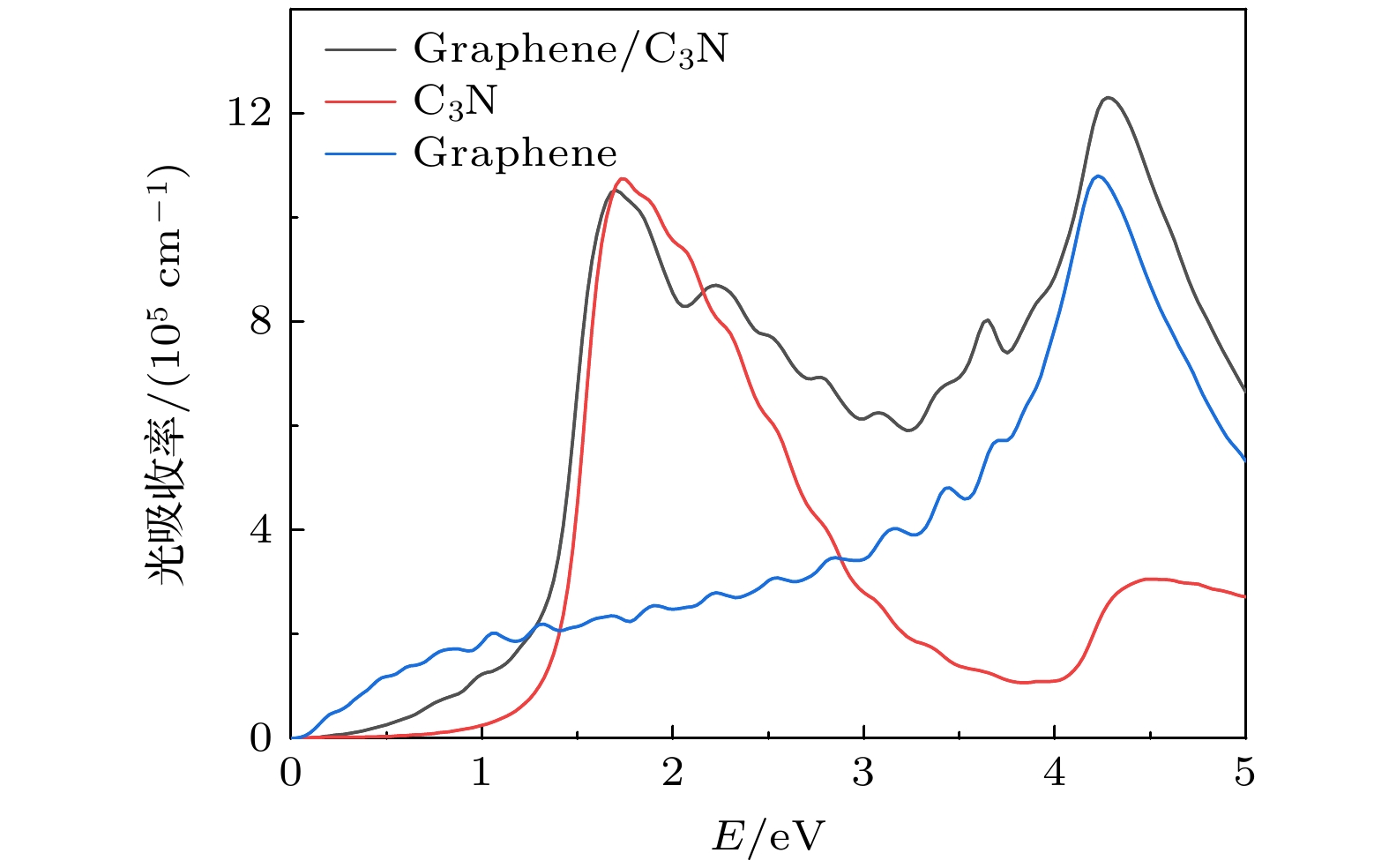
图 6 单层Gr、单层C3N和Gr/C3N vdWH的光吸收率
Figure 6. The optical absorbance of monolayer Gr, monolayer C3N, and Gr/C3N vdWH.
-
[1] Novoselov K S, Geim A K, Morozov S V, Jiang D E, Zhang Y, Dubonos S V, Grigorieva I V, Firsov A A 2004 Science 306 666
Google Scholar
[2] Nandanapalli K R, Mudusu D, Lee S 2019 Carbon 152 954
Google Scholar
[3] Aditya D G, Abhay R S, Vilasrao J K 2017 Current Drug Targets. 18 724
Google Scholar
[4] Neto A C, Guinea F, Peres N M, Novoselov K S, Geim A K 2009 Rev. Mod. Phys. 81 109
Google Scholar
[5] Liu S X, Li Z J, Ge Y Q, Wang H D, Yue R, Jiang X T, Li J Q, Wen Q, Zhang H 2017 Photonics Res. 5 662
Google Scholar
[6] Mahmood J, Lee E K, Jung M, Shin D, Choi H J, Seo J M, Jung S M, Kim D, Li F, Lah M S, Park N, Shin H J, Oh J H, Baek J B 2016 Proc. Natl. Acad. Sci. 113 7414
Google Scholar
[7] Li X L, Wang X R, Zhang L, Lee S W, Dai H J 2008 Science 319 1229
Google Scholar
[8] Son J, Lee S, Kim S J, Park B C, Lee H K, Kim S, Kim J H, Hong B H, Hong J 2016 Nat. Commun. 7 13261
Google Scholar
[9] Fan X F, Shen Z X, Liu A Q, Kuo J L 2012 Nanoscale 4 2157
Google Scholar
[10] Shinde P P, Kumar V 2011 Phys. Rev. B 84 125401
Google Scholar
[11] Cui Z, Ren K, Zhao Y M, Wang X, Shu H B, Yu J, Tang W C, Sun M L 2019 Appl. Surf. Sci. 492 513
Google Scholar
[12] Chen D C, Lei X L, Wang Y N, Zhong S Y, Liu G, Xu B, Ouyang C Y 2019 Appl. Surf. Sci. 497 143809
Google Scholar
[13] Pierucci D, Henck H, Avila J, Balan A, Naylor C H, Patriarche G, Dappe Y J, Silly M G, Sirotti F, Johnson A C 2016 Nano. Lett. 16 4054
Google Scholar
[14] Chen H, Zhao J, Huang J, Liang Y 2019 Phys. Chem. Chem. Phys. 21 7447
Google Scholar
[15] Pham K D, Hieu N N, Phuc H V, Fedorov I A, Duque C A, Amin B, Nguyen C V 2018 Appl. Phys. Lett. 113 171605
Google Scholar
[16] Allain A, Kang J, Banerjee K, Kis A 2015 Nat. Mater. 14 1195
Google Scholar
[17] Mott N F 1939 MPS 171 27
[18] Tung R T 2014 Appl. Phys. Rev. 1 011304
Google Scholar
[19] Liu Y, Guo J, Zhu E B, Liao L, Lee S J, Ding M N, Shakir I, Gambin V, Huang Y, Duan X F 2018 Nature 557 696
Google Scholar
[20] Bardeen J 1947 Phys. Rev. 71 717
Google Scholar
[21] Hasegawa H, Sawada T 1983 Thin Solid Films 103 119
Google Scholar
[22] Amsalem P, Niederhausen J, Wilke A, Heimel G, Schlesinger R, Winkler S, Vollmer A, Rabe J, Koch N 2013 Phys. Rev. B 87 035440
Google Scholar
[23] Zhou X, Hu X Z, Zhou S S, Song H Y, Zhang Q, Pi L J, Li L, Li H Q, Lü J T, Zhai T Y 2018 Adv. Mater. 30 1703286
Google Scholar
[24] Guo J, Wang L Y, Yu Y W, Wang P Q, Huang Y, Duan X F 2019 Adv. Mater. 31 1902962
Google Scholar
[25] Zheng D Q, Zhao Z, Huang R, Nie J, Li L, Zhang Y 2017 Nano. Energy 32 448
Google Scholar
[26] Yang S W, Li W, Ye C C, Wang G, Tian H, Zhu C, He P, Ding G Q, Xie X M, Liu Y, Lifshitz Y, Lee S T, Kang Z H, Jiang M H 2017 Adv. Mater. 29 1605625
Google Scholar
[27] Kang D W, Zuo Z W, Zhang S, Wang Z W, Zhang L L 2020 Appl. Phys. Lett. 116 153103
Google Scholar
[28] Zhao J, Zeng H, Zhou X 2019 Carbon 145 1
Google Scholar
[29] Brandbyge M, Mozos J L, Ordejón J, Taylor J, Stokbro K 2002 Phys. Rev. B 65 165401
Google Scholar
[30] Deng Y X, Chen S Z, Zeng Y, Feng Y, Zhou W X, Tang L M, Chen K Q 2018 Org. Electron. 63 310
Google Scholar
[31] Liu H R, Gao R, Yang J E, Yang F, Wang T X, Zhang Z X, Liu X G, Jia H S, Xu B S, Ma H 2020 Appl. Surf. Sci. 525 146476
Google Scholar
[32] Yazyev O V, Louie S G 2010 Phys. Rev. B 81 195420
Google Scholar
[33] Zhang D B, Hu Y, Zhong H X, Yuan S J, Liu C 2019 Nanoscale 11 13800
Google Scholar
[34] Hu Q, Wu Q, Wang H, He J, Zhang G 2012 Phys. Status Solidi (b) 249 784
Google Scholar
[35] Gao X, Shen Y, Ma Y, Wu S, Zhou Z 2019 Comput. Mater Sci. 170 109200
Google Scholar
[36] Nguyen C V, Idrees M, Phuc H V, Hieu N N, Binh N T, Amin B, Vu T V 2020 Phys. Rev. B 101 235419
Google Scholar
[37] Xiong W X, Xia C X, Zhao X, Wang T X, Jia Y 2016 Carbon 109 737
Google Scholar
[38] Gao X, Shen Y Q, Ma Y Y, Wu S Y, Zhou Z X 2019 Carbon 146 337
Google Scholar
[39] Zhang W, Hao G, Zhang R, Xu J, Ye X, Li H 2021 Phys. Chem. Solids 157 110189
Google Scholar
[40] Zeng H, Chen R S, Yao G 2020 Adv. Electron. Mater. 6 1901024
Google Scholar
[41] Xu H, Wu J, Chen Y, Zhang H, Zhang J 2013 Chem. Asian J. 8 2446
Google Scholar
[42] Kim S M, Hsu A, Araujo P, Lee Y H, Palacios T S, Dresselhaus M, Idrobo J C, Kim K K, Kong J 2013 Nano Lett. 13 933
Google Scholar
[43] Liu H, Chen X, Deng L, Su X, Guo K, Zhu Z 2016 Electrochim. Acta 206 184
Google Scholar
[44] Hou C, Tai G A, Liu B, Wu Z H, Yin Y H 2021 Nano Res. 14 2337
Google Scholar
[45] Yin H F, Cao Y, Fan T L, Zhang M, Yao J C, Li P F, Chen S M, Liu X H 2021 Sci. Total Environ. 754 141926
Google Scholar
[46] Liu Y, Chen P, Chen Y, Lu H, Wang J, Yang Z, Lu Z, Li M, Fang L 2016 RSC Adv. 6 10802
Google Scholar
[47] Alcudia-Ramos M, Fuentez-Torres M, Ortiz-Chi F, Espinosa-González C, Hernández-Como N, García-Zaleta D, Kesarla M, Torres-Torres J, Collins-Martínez V, Godavarthi S 2020 Ceram. Int. 46 38
Google Scholar
[48] Mak K F, Shan J 2016 Nat. Photonics 10 216
Google Scholar
[49] Qi S M, Jiang J W, Wang X C, Mi W B 2021 Carbon 174 540
Google Scholar
[50] Phuc H V, Hieu N N, Hoi B D, Nguyen C V 2018 Phys. Chem. Chem. Phys. 20 17899
Google Scholar
[51] Zeng H, Zhao J, Cheng A Q, Zhang L, He Z, Chen R S 2018 Nanotechnology 29 075201
Google Scholar
[52] Mohanta M K, Sarkar A D 2021 Appl. Surf. Sci. 540 148389
Google Scholar
[53] Lee G H, Yu Y J, Cui X, Petrone N, Lee C H, Choi M S, Lee D Y, Lee C, Yoo W J, Watanabe K, Taniguchi T, Nuckolls C, Kim P, Hone J 2013 ACS Nano 7 9
[54] Vu T V, Hieu N V, Phuc H V, Hieu N N, Bui H, Idrees M, Amin B, Nguyen C V 2020 Appl. Surf. Sci. 507 145036
Google Scholar
[55] Yankowitz M, Watanabe K, Taniguchi T, San-Jose P, LeRoy B J 2016 Nat. Commun. 7 13168
Google Scholar
[56] Fülöp B, Márffy A, Tóvári E, Kedves M, Zihlmann S, Indolese D, Kovács-Krausz Z, Watanabe K, Taniguchi T, Schönenberger C, Kézsmárki I, Makk P, Csonka S 2021 J. Appl. Phys. 130 064303
Google Scholar
[57] Cho C, Wong J, Taqieddin A, Biswas S, Aluru N R, Nam S, Atwater H A 2021 Nano Lett. 21 3956
Google Scholar
[58] Tongay S, Fan W, Kang J, Park J, Koldemir U, Suh J, Narang D S, Liu K, Ji J, Li J, Sinclair R, Wu J 2014 Nano Lett. 14 3185
Google Scholar
[59] Fang H, Battaglia C, Carraro C, Nemsak S, Ozdol B, Kang J S, Bechtel H A, Desai S B, Kronast F, Unal A A, Conti C, Conlon C, Palsson G K, Martin M C, Minor A M, Fadley C S, Yablonovitch E, Maboudian R, Javey A 2014 Natl. Acad. Sci. 111 6198
Google Scholar
[60] Hu W, Li Z, Yang J 2013 Jpn. J. Appl. Phys. 139 154704
[61] Deng S, Li L, Rees P 2019 ACS Appl. Nano. Mater 2 3977
Google Scholar
[62] Gao X, Shen Y Q, Ma Y Y, Wu S Y, Zhou Z X 2019 Appl. Surf. Sci. 479 1098
Google Scholar

 DownLoad:


Catalog
Metrics
- Abstract views: 1606
- PDF Downloads: 57
- Cited By: 0
