


-
Photovoltaic device based on van der Waals heterojunction provides an effective way to develop high-performance, low-power consumption, ultra-integrated micro photodetection system. In this paper, we construct an asymmetric Au/MoS2 Schottky junction to realize a planar MoS2-based photovoltaic device. In order to further improve the photoelectric performance of the device, we design a structure covering MoO3 on the surface of MoS2 to construct the heterojunction. Owing to the absorption properties of MoO3 in visible light and the excellent light transmittance of the ultra-thin two-dimensional structure, the electrons involved in conducting in MoS2 material are increased. In most of previous reports, the preparation methods and performance improvement of MoS2/MoO3 heterojunctions were the focus of research, but little attention was paid to exploring the influence of overlayer on devices. Therefore, in this work, we investigate the influence of overlayer thickness on device performance. With the help of atomic layer deposition (ALD) method to control the film thickness, each of the MoO3 materials with thickness of 4 nm, 12 nm and 20 nm (deposition periods of 10, 30 and 50, respectively) is covered on the surface of a MoS2-based photodetector. The photoelectric performance enhancement effects of three groups of heterojunction photodetectors are compared with each other. The results show that the thinner the MoO3 layer, the more significant the enhancement effect of heterojunction photodetectors is. This is mainly attributed to the fact that ultra-thin MoO3 layer not only has visible light absorption, but also reduces the influence of the covering layer on the light absorption of MoS2, thus achieving a heterojunction system with high light absorption efficiency. In addition, the interfacial electric field of the heterojunction effectively promotes the separation of photogenerated carriers, and the thinner the MoO3 coating layer, the weaker the effect of introducing the interfacial defects of the heterojunction is. Therefore, the dark current gain effect of the device is effectively suppressed, which is beneficial to improving the response speed and optical detectivity of the device. Comparing with pure MoS2 photovoltaic photodetectors, the photoresponsivity of MoS2/MoO3 heterojunction device in this paper is enhanced nearly 10 times. The device exhibits a high photoresponse of ~916.121 A/W, a detectivity of ~2.74×10¹¹ Jones, and a fast response time of ~73 μs, showing that this design can effectively solve the low-responsiveness problem of planar photovoltaic device. In this study, for the first time, we construct a planar photovoltaic device based on MoS2/MoO3. By designing heterostructure and optimizing the thickness of the overlayer, the photoelectric performance of planar MoS2-based photovoltaic device is successfully improved, which provides a reference scheme for developing high-performance heterojunction photodetectors of MoS2/oxide materials in future.
-
Keywords:
- MoS2 /
- MoO3 /
- heterojunction /
- photovoltaic photodetector
[1] Lu J T, Zheng Z Q, Yao J D, Gao W, Xiao Y, Zhang M L, Li J B 2020 Nanoscale 12 7196
 Google Scholar
[2] Wang J, Han J Y, Chen X Q, Wang X R 2019 InfoMat 1 33
Google Scholar
[3] Liu B S, Zhang X K, Du J L, Xiao J K, Yu H H, Hong M Y, Gao L, Ou Y, Kang Z, Liao Q L, Zhang Z, Zhang Y 2022 InfoMat 4 12282
Google Scholar
[4] Yoo G, Hong S, Heo J, Kim S 2017 Appl. Phys. Lett. 110 053112
Google Scholar
[5] Zhang H, Wang Z H, Chen J W, Tan C Y, Yin S Q, Zhang H L, Wang S T, Qin Q G, Li L 2022 Nanoscale 14 16130
Google Scholar
[6] Wang Z H, Zhang H, Wang W K, Tan C Y, Chen J W, Yin S Q, Zhang H L, Zhu A K, Li G, Du Y C, Wang S T, Liu F G, Li L 2022 ACS Appl. Mater. Interfaces 14 37926
Google Scholar
[7] Zhou C J, Raju S, Li B, Chan M, Chai Y, Yang C Y 2018 Adv. Funct. Mater. 28 1802954
Google Scholar
[8] Zhao Y D, Xiao X Y, Huo Y J, Wang Y C, Zhang T F, Jiang K L, Wang J P, Fan S S, Li Q Q 2017 ACS Appl. Mater. Interfaces 9 18945
Google Scholar
[9] Kang Z, Cheng Y F, Zheng Z, Cheng F, Chen Z Y, Li L Y, Tan X Y, Xiong L, Zhai T Y, Gao Y J 2019 Nano-Micro Lett. 11 34
Google Scholar
[10] Tang X Q, Wang S, Liang Y, Bai D W, Xu J Y, Wang Y Y, Chen C Y, Liu X, Wu S M, Wen Y, Jiang D Y, Zhang Z H 2022 Phys. Chem. Chem. Phys. 24 7323
Google Scholar
[11] Shi K X, Li J H, Xiao Y C, Guo L, Chu X Y, Zhai Y J, Zhang B L, Lu D X, Rosei F 2020 ACS Appl. Mater. Interfaces 12 31382
Google Scholar
[12] Du P, Fang X, Zhao H B, Fang D, Wang D B, Gong Q, Kou X F, Liu X L, Wang X H 2020 J. Alloys Compd. 847 156390
Google Scholar
[13] Zhang B W, Fang D, Fang X, Zhao H B, Wang D K, Li J H, Wang X H, Wang D B 2022 Rare Met. 41 982
Google Scholar
[14] Du P, Fang X, Gong Q, Li J M, Kou X F, Zhao H B, Wang X H 2019 Phys. Status Solidi RRL 13 1900474
Google Scholar
[15] Wang Z, Xia H, Wang P, Zhou X H, Liu C S, Zhang Q H, Wang F, Huang M L, Chen S Y, Wu P S, Chen Y F, Ye J F, Huang S Y, Yan H G, Gu L, Miao J S, Li T X, Chen X S, Lu W, Zhou P, Hu W D 2021 Adv. Mater. 33 2104942
Google Scholar
[16] Chen Y F, Tan C W, Wang Z, Miao J S, Ge X, Zhao T G, Liao K C, Ge H N, Wang Y, Wang F, Zhou Y, Wang P, Zhou X H, Shan C X, Peng H L, Hu W D 2022 Sci. Adv. 8 eabq1781
Google Scholar
[17] Shan J J, Li J H, Chu X Y, Xu M Z, Jin F J 2018 IOP Conf. Ser. Mater. Sci. Eng. 382 022070
Google Scholar
[18] Zhang R J, Ma X L, An C H, Zhang D H, Sun D, Hu X D, Liu J 2019 2 D Mater. 6 035033
Google Scholar
[19] 毕开西, 万强, 舒志文, 邵功磊, 靳媛媛, 朱梦剑, 林均, 刘华伟, 刘怀志, 陈艺勤, 刘松, 段辉高 2020 中国科学-材料 63 1076
Google Scholar
Bi K X, Wan Q, Shu Z W, Shao G L, Jin Y Y, Zhu M J, Lin J, Liu H W, Liu H Z, Chen Y Q, Liu S, Duan H G 2020 Sci. China Mater. 63 1076
Google Scholar
[20] Guo Y X, Kang L X, Song P, Zeng Q S, Tang B J, Yang J F, Wu Y, Tian D, Xu M Z, Zhao W, Qi X F, Zhang Z Y, Liu Z 2021 2D Mater. 8 035036
Google Scholar
[21] Pala S, Mukherjee S, Nand M, Srivastava H, Mukherjee C, Jha S N, Ray S K 2020 App. Surf. Sci. 502 144196
Google Scholar
[22] Feng S, Liu C, Zhu Q B, Su X, Qian W W, Sun Y, Wang C X, Li B, Chen M L, Chen L, Chen W, Zhang L L, Zhen C, Wang F J, Ren W C, Yin L C, Wang X M, Cheng H M, Sun D M 2021 Nat. Commun. 12 4094
Google Scholar
[23] Liu X X, Li F, Xu M X, Shen T, Yang Z L, Fan W L, Qi J J 2018 Langmuir 34 14151
Google Scholar
[24] Nalwa H S 2020 RSC Adv. 10 30529
Google Scholar
[25] Wang Y, Du X, Wang J M, Su M Z, Wan X, Meng H, Xie W G, Xu J B, Liu P Y 2017 ACS Appl. Mater. Interfaces 9 5543
Google Scholar
[26] Seguin L, Figlarz M, Cavagnat R, Lasskgues J C 1995 Spectrochim. Acta A Mol. Biomol. Spectrosc. 51 1323
Google Scholar
[27] Demirtas M, Odacı C, Shehu Y, Perkgöz N K, Ay F 2020 Mater. Sci. Semicon. Proc. 108 104880
Google Scholar
[28] Xu H Y, Akbari M K, Hai Z Y, Wei Z H, Hyde L, Verpoort F, Xue C Y, Zhuiykov S 2018 Mater. Design 149 135
Google Scholar
[29] Dai T J, Ren Y X, Qian L X, Liu X Z 2018 J. Electron. Mater. 47 6709
Google Scholar
[30] Choi J H, Lee S W, Kim H B, Ahn J H 2020 Appl. Surf. Sci. 532 147462
Google Scholar
[31] Choi Y, Kim Y, Jung E, Oh M, Kim H 2014 J. Korean Phys. Soc. 64 1535
Google Scholar
[32] Rezeq M, Ali A, Patole S P, Eledlebi K, Dey R K, Cui B 2018 AIP Adv. 8 055122
Google Scholar
[33] Zhang Z G 2010 Chin. Phys. B 19 127802
Google Scholar
[34] Schulz P, Cowan S R, Guan Z L, Garcia A, Olson D C, Kahn A 2014 Adv. Funct. Mater. 24 701
Google Scholar
[35] Yu Y L, Shen T, Long H R, Zhong M Z, Xin K Y, Zhou ZQ, Wang X Y, Liu Y Y, Wakabayashi H, Liu L Y, Yang J H, Wei Z M, Deng H X 2022 Adv. Mater. 34 2206486
Google Scholar
[36] Zhang W J, Chuu C P, Huang J K, Chen C H, Tsai M L, Chang Y H, Liang C T, Chen Y Z, Chueh Y L, He J H, Chou M Y, Li L J 2014 Sci. Rep. 4 3826
Google Scholar
[37] Lin J D, Han C, Wang F, Wang R, Xiang D, Qing S, Zhang X A, Wang L, Zhang H, Wee A T S, Chen W 2014 ACS Nano 8 5323
Google Scholar
[38] Zhang K N, Zhang T N, Cheng G H, Li T X, Wang S X, Wei W, Zhou X H, Yu W W, Sun Y, Wang P, Zhang D, Zeng C G, Wang X J, Hu W D, Fan H J, Shen G Z, Chen X, Duan X F, Chang K, Dai N 2016 ACS Nano 10 3852
Google Scholar
[39] Im H, Liu N, Bala A, Kim S, Choi W 2019 APL Mater. 7 061101
Google Scholar
[40] Wei Y F, Tran V T, Zhao C Y, Liu H F, Kong J H, Du H J 2019 ACS Appl. Mater. Interfaces 11 21445
Google Scholar
[41] Gunasekaran S, Marnadu R, Thangaraju D, Chandrasekaran J, Hegazy H H, Somaily H H, Durairajan A, Valente M A, Elango M, Reddy V R M 2021 Mater. Sci. Semicon. Proc. 135 106097
Google Scholar
-
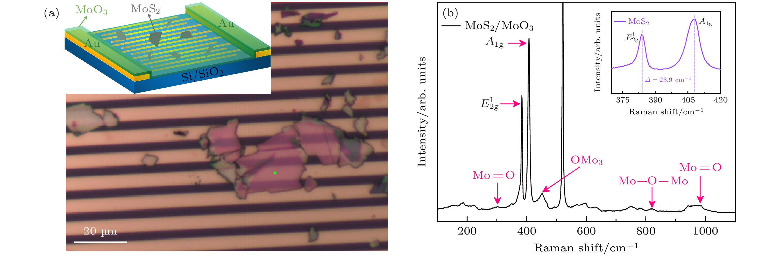
图 1 (a) MoS2/MoO3光伏型光电探测器的光学形貌图, 插图为器件模型图; (b) MoS2/MoO3异质结的Raman光谱, 插图为MoS2薄膜的Raman光谱
Figure 1. (a) Optical morphology diagram of MoS2/MoO3 photovoltaic photodetector, the inset shows model diagram; (b) Raman spectra of MoS2/MoO3 heterojunction, the inset shows Raman spectra of MoS2 film.

图 2 (a)—(c)3组MoS2光电探测器在532 nm激光辐照下的I-V曲线, 图(a)中插图为灰色箭头指示处的I-V曲线放大视图; (d)—(f) 分别在图(a)—(c)中样品表面沉积10, 30, 50个周期MoO3后的MoS2/MoO3光电探测器的I-V曲线
Figure 2. (a)–(c) I-V curves of three MoS2 photodetectors, the laser incident at 532 nm, the inset shows an enlarged view of I-V curve at the gray arrow; (d)–(f) the I-V curves of MoS2/MoO3 photodetectors after 10, 30, and 50 cycles of MoO3 were deposited on the sample surface in Fig. (a)–(c), respectively.
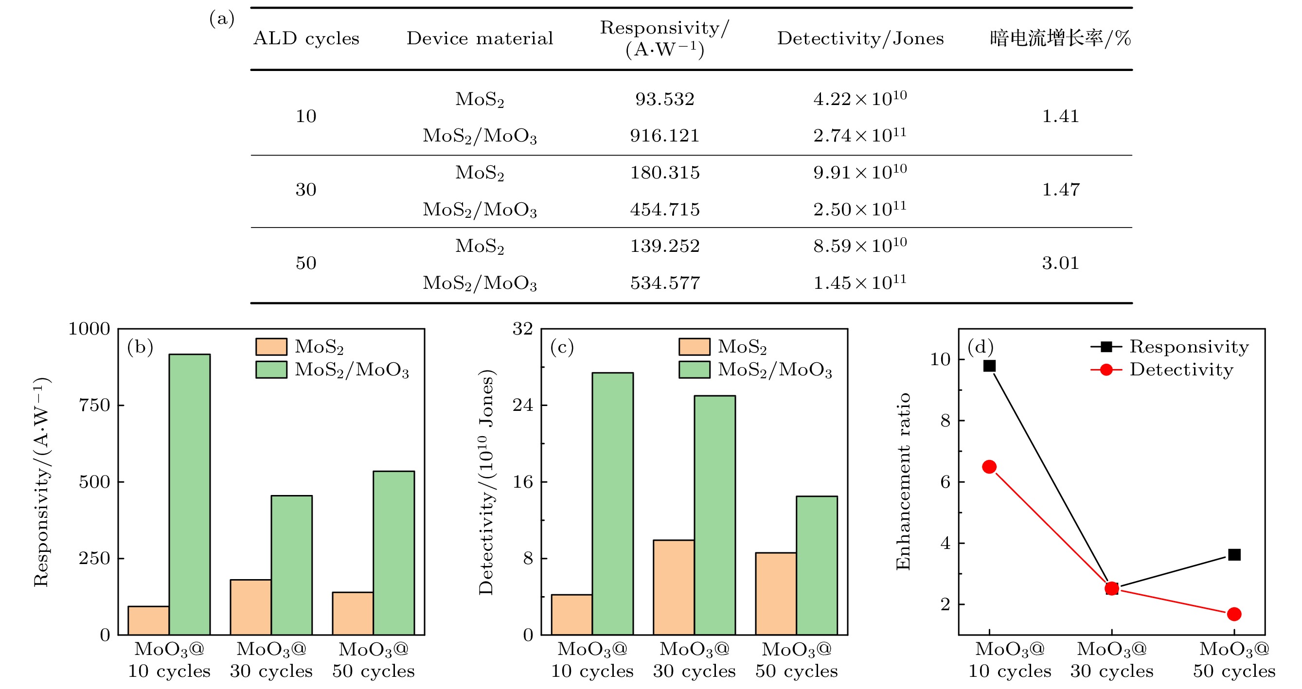
图 3 覆盖层不同厚度的MoS2/MoO3光电探测器 (a)性能对比; (b) 响应度对比; (c) 探测率对比; (d) 光电性能增强倍数对比
Figure 3. (a) Performance comparison; (b) responsivity comparison; (c) detectivity comparison; (d) performance enhancement ratio comparison of MoS2/MoO3 photodetectors with different thickness of the overlayer.

图 4 (a) 光伏性能测试系统示意图; (b)光辐照下器件Au/MoS2肖特基结能带图; (c), (d) MoS2光电探测器和MoS2/MoO3光电探测器在不同激光功率密度下的光伏曲线; (e), (f) 不同功率密度下, MoS2复合MoO3前后(e)光伏数据对比和(f)器件响应时间对比
Figure 4. (a) The testing process of photovoltaic performance; (b) band diagram of Au/MoS2 electrodes asymmetrical contact under illumination; (c), (d) photovoltaic curves of MoS2 and MoS2/MoO3 photodetectors at different laser power densities; (e), (f) photovoltaic performance and photoresponse times comparison of MoS2 and MoS2/MoO3 photodetectors under different power densities.

图 5 (a) MoO3的吸收; (b) MoO3的带隙, 红线是提取带隙的辅助线; (c) MoS2与MoO3构成异质结前的能带图; (d) MoS2与MoO3@10 cycles构成异质结后的能带变化图, 其中红色小球代表光生电子, 绿色小球代表光生空穴, 蓝色箭头代表异质结内建电场的方向, 灰色箭头代表载流子的移动方向; (e) MoS2复合MoO3前后的Raman和PL光谱对比
Figure 5. (a) The absorption of the MoO3; (b) the bandgap of the MoO3, the red line is an auxiliary line for extracting bandgap; (c) band diagram of MoS2 and MoO3 before heterojunction formed; (d) band diagram of MoS2 and MoO3 after heterojunction formed. Red balls represent photoelectrons, green balls represent light holes, blue arrows represent the direction of the built electric field within the heterojunction and gray arrows represent the direction of the carrier movement; (e) Raman and PL spectra of MoS2 in individual and heterostructures.
表 1 本文器件与其他MoS2/MoO3基光电器件的性能与MoO3制备方法比较
Table 1. Comparison of MoS2/MoO3 photodetectors performance and MoO3 preparation.
材料 光伏器件 MoO3制备方法 响应时间/μs 探测率/Jones 响应度/(A·W–1) 文献 MoS2/MoO3 Yes ALD 73 2.74×10¹¹ 916.121 本工作 MoS2/MoOX No 热蒸发 3.52×10⁶ — 65.2 [4] MoS2/MoO3/Graphene Yes 电子束蒸发 102 4.77×10¹⁰ 0.67 [18] MoS2/MoOX No 化学氧化 9×10⁵ — 3.6×10⁻³ [19] MoS2/MoO3/p-Si Yes 自然氧化 6×10⁵ 2.8×10¹¹ 0.16 [21] MoS2/α-MoOX No CVD 95 9.8×10¹⁶ 105 [22] MoS2/MoOX No CVD 9.8×10⁶ 2.08×10¹¹ 1.09 [39] MoS2/MoO3 No 化学剥离 1.75×10⁷ — 0.134×10⁻³ [40] MoO3@MoS2/p-Si Yes 化学沉淀 — 5.813×10¹⁰ 9.23×10⁻³ [41]  DownLoad: CSV
-
[1] Lu J T, Zheng Z Q, Yao J D, Gao W, Xiao Y, Zhang M L, Li J B 2020 Nanoscale 12 7196
Google Scholar
[2] Wang J, Han J Y, Chen X Q, Wang X R 2019 InfoMat 1 33
Google Scholar
[3] Liu B S, Zhang X K, Du J L, Xiao J K, Yu H H, Hong M Y, Gao L, Ou Y, Kang Z, Liao Q L, Zhang Z, Zhang Y 2022 InfoMat 4 12282
Google Scholar
[4] Yoo G, Hong S, Heo J, Kim S 2017 Appl. Phys. Lett. 110 053112
Google Scholar
[5] Zhang H, Wang Z H, Chen J W, Tan C Y, Yin S Q, Zhang H L, Wang S T, Qin Q G, Li L 2022 Nanoscale 14 16130
Google Scholar
[6] Wang Z H, Zhang H, Wang W K, Tan C Y, Chen J W, Yin S Q, Zhang H L, Zhu A K, Li G, Du Y C, Wang S T, Liu F G, Li L 2022 ACS Appl. Mater. Interfaces 14 37926
Google Scholar
[7] Zhou C J, Raju S, Li B, Chan M, Chai Y, Yang C Y 2018 Adv. Funct. Mater. 28 1802954
Google Scholar
[8] Zhao Y D, Xiao X Y, Huo Y J, Wang Y C, Zhang T F, Jiang K L, Wang J P, Fan S S, Li Q Q 2017 ACS Appl. Mater. Interfaces 9 18945
Google Scholar
[9] Kang Z, Cheng Y F, Zheng Z, Cheng F, Chen Z Y, Li L Y, Tan X Y, Xiong L, Zhai T Y, Gao Y J 2019 Nano-Micro Lett. 11 34
Google Scholar
[10] Tang X Q, Wang S, Liang Y, Bai D W, Xu J Y, Wang Y Y, Chen C Y, Liu X, Wu S M, Wen Y, Jiang D Y, Zhang Z H 2022 Phys. Chem. Chem. Phys. 24 7323
Google Scholar
[11] Shi K X, Li J H, Xiao Y C, Guo L, Chu X Y, Zhai Y J, Zhang B L, Lu D X, Rosei F 2020 ACS Appl. Mater. Interfaces 12 31382
Google Scholar
[12] Du P, Fang X, Zhao H B, Fang D, Wang D B, Gong Q, Kou X F, Liu X L, Wang X H 2020 J. Alloys Compd. 847 156390
Google Scholar
[13] Zhang B W, Fang D, Fang X, Zhao H B, Wang D K, Li J H, Wang X H, Wang D B 2022 Rare Met. 41 982
Google Scholar
[14] Du P, Fang X, Gong Q, Li J M, Kou X F, Zhao H B, Wang X H 2019 Phys. Status Solidi RRL 13 1900474
Google Scholar
[15] Wang Z, Xia H, Wang P, Zhou X H, Liu C S, Zhang Q H, Wang F, Huang M L, Chen S Y, Wu P S, Chen Y F, Ye J F, Huang S Y, Yan H G, Gu L, Miao J S, Li T X, Chen X S, Lu W, Zhou P, Hu W D 2021 Adv. Mater. 33 2104942
Google Scholar
[16] Chen Y F, Tan C W, Wang Z, Miao J S, Ge X, Zhao T G, Liao K C, Ge H N, Wang Y, Wang F, Zhou Y, Wang P, Zhou X H, Shan C X, Peng H L, Hu W D 2022 Sci. Adv. 8 eabq1781
Google Scholar
[17] Shan J J, Li J H, Chu X Y, Xu M Z, Jin F J 2018 IOP Conf. Ser. Mater. Sci. Eng. 382 022070
Google Scholar
[18] Zhang R J, Ma X L, An C H, Zhang D H, Sun D, Hu X D, Liu J 2019 2 D Mater. 6 035033
Google Scholar
[19] 毕开西, 万强, 舒志文, 邵功磊, 靳媛媛, 朱梦剑, 林均, 刘华伟, 刘怀志, 陈艺勤, 刘松, 段辉高 2020 中国科学-材料 63 1076
Google Scholar
Bi K X, Wan Q, Shu Z W, Shao G L, Jin Y Y, Zhu M J, Lin J, Liu H W, Liu H Z, Chen Y Q, Liu S, Duan H G 2020 Sci. China Mater. 63 1076
Google Scholar
[20] Guo Y X, Kang L X, Song P, Zeng Q S, Tang B J, Yang J F, Wu Y, Tian D, Xu M Z, Zhao W, Qi X F, Zhang Z Y, Liu Z 2021 2D Mater. 8 035036
Google Scholar
[21] Pala S, Mukherjee S, Nand M, Srivastava H, Mukherjee C, Jha S N, Ray S K 2020 App. Surf. Sci. 502 144196
Google Scholar
[22] Feng S, Liu C, Zhu Q B, Su X, Qian W W, Sun Y, Wang C X, Li B, Chen M L, Chen L, Chen W, Zhang L L, Zhen C, Wang F J, Ren W C, Yin L C, Wang X M, Cheng H M, Sun D M 2021 Nat. Commun. 12 4094
Google Scholar
[23] Liu X X, Li F, Xu M X, Shen T, Yang Z L, Fan W L, Qi J J 2018 Langmuir 34 14151
Google Scholar
[24] Nalwa H S 2020 RSC Adv. 10 30529
Google Scholar
[25] Wang Y, Du X, Wang J M, Su M Z, Wan X, Meng H, Xie W G, Xu J B, Liu P Y 2017 ACS Appl. Mater. Interfaces 9 5543
Google Scholar
[26] Seguin L, Figlarz M, Cavagnat R, Lasskgues J C 1995 Spectrochim. Acta A Mol. Biomol. Spectrosc. 51 1323
Google Scholar
[27] Demirtas M, Odacı C, Shehu Y, Perkgöz N K, Ay F 2020 Mater. Sci. Semicon. Proc. 108 104880
Google Scholar
[28] Xu H Y, Akbari M K, Hai Z Y, Wei Z H, Hyde L, Verpoort F, Xue C Y, Zhuiykov S 2018 Mater. Design 149 135
Google Scholar
[29] Dai T J, Ren Y X, Qian L X, Liu X Z 2018 J. Electron. Mater. 47 6709
Google Scholar
[30] Choi J H, Lee S W, Kim H B, Ahn J H 2020 Appl. Surf. Sci. 532 147462
Google Scholar
[31] Choi Y, Kim Y, Jung E, Oh M, Kim H 2014 J. Korean Phys. Soc. 64 1535
Google Scholar
[32] Rezeq M, Ali A, Patole S P, Eledlebi K, Dey R K, Cui B 2018 AIP Adv. 8 055122
Google Scholar
[33] Zhang Z G 2010 Chin. Phys. B 19 127802
Google Scholar
[34] Schulz P, Cowan S R, Guan Z L, Garcia A, Olson D C, Kahn A 2014 Adv. Funct. Mater. 24 701
Google Scholar
[35] Yu Y L, Shen T, Long H R, Zhong M Z, Xin K Y, Zhou ZQ, Wang X Y, Liu Y Y, Wakabayashi H, Liu L Y, Yang J H, Wei Z M, Deng H X 2022 Adv. Mater. 34 2206486
Google Scholar
[36] Zhang W J, Chuu C P, Huang J K, Chen C H, Tsai M L, Chang Y H, Liang C T, Chen Y Z, Chueh Y L, He J H, Chou M Y, Li L J 2014 Sci. Rep. 4 3826
Google Scholar
[37] Lin J D, Han C, Wang F, Wang R, Xiang D, Qing S, Zhang X A, Wang L, Zhang H, Wee A T S, Chen W 2014 ACS Nano 8 5323
Google Scholar
[38] Zhang K N, Zhang T N, Cheng G H, Li T X, Wang S X, Wei W, Zhou X H, Yu W W, Sun Y, Wang P, Zhang D, Zeng C G, Wang X J, Hu W D, Fan H J, Shen G Z, Chen X, Duan X F, Chang K, Dai N 2016 ACS Nano 10 3852
Google Scholar
[39] Im H, Liu N, Bala A, Kim S, Choi W 2019 APL Mater. 7 061101
Google Scholar
[40] Wei Y F, Tran V T, Zhao C Y, Liu H F, Kong J H, Du H J 2019 ACS Appl. Mater. Interfaces 11 21445
Google Scholar
[41] Gunasekaran S, Marnadu R, Thangaraju D, Chandrasekaran J, Hegazy H H, Somaily H H, Durairajan A, Valente M A, Elango M, Reddy V R M 2021 Mater. Sci. Semicon. Proc. 135 106097
Google Scholar

 DownLoad:
Catalog
Metrics
- Abstract views: 1938
- PDF Downloads: 63
- Cited By: 0
