


-
Memtransistor is a new multi-terminal device which combines the properties of memristor and field effect transistor and simultaneously realizes information storage and processing. In this paper, the multilayer MoS2 is prepared by micromechanical exploration method, then the back gate MoS2 memtransistor with field effect transistor structure is fabricated, and the resistive switching characteristics and mechanism of the device under electric field, light field and their synergistic regulation are systematically studied. The experimental results show that the multilayer MoS2 memtransistor has excellent bipolar resistance behavior and good cycle durability. Under the control of gate voltage, the switching ratio of the device can be tuned in a range of 100-105, up to 1.56 × 10⁵, which indicates that the device has a strong gating effect. Under the control of light illumination, the resistance characteristics of the device are strongly dependent on the incident wavelength. When photoelectric synergistic regulation is performed, the device displays excellent four-terminal control capability, and the switching ratio is enhanced up to 4.8 × 10⁴. The mechanism of resistive switching characteristics can be attributed to the changes of charge capture state and Schottky barrier height at the interface between MoS2 and metal electrodes, and the continuous photoconductance effect caused by photogenerated carriers in MoS2 channel.
-
Keywords:
- MoS2 /
- memtransistor /
- memristor /
- resistance switch characteristic
[1] Lu H, Seabaugh A 2014 IEEE J. Electron Devices Soc. 2 44
 Google Scholar
[2] Sangwan V K, Lee H S, Bergeron H, Balla I, Beck M E, Chen K S, Hersam M C 2018 Nature 554 500
Google Scholar
[3] Yin S Q, Song C, Sun Y M, Qiao L L, Wang B L, Sun Y F, Liu K, Pan F, Zhang X Z 2019 ACS Appl. Mater. Interfaces 11 43344
Google Scholar
[4] Wang L, Liao W G, Wong S L, Yu Z G, Li S F, Lim Y F, Feng X W, Tan W C, Huang X, Chen L, Liu L, Chen J S, Gong X, Zhu C X, Liu X K, Zhang Y W, Chi D Z, Ang K W 2019 Adv. Funct. Mater. 29 1901106
Google Scholar
[5] Lee H S, Sangwan V K, Rojas W A G, Bergeron H, Jeong H Y, Yuan J T, Su K, Hersam M C 2020 Adv. Funct. Mater. 30 2003683
Google Scholar
[6] Yang Y, Du H Y, Xue Q, Wei X H, Yang Z B, Xu C G, Lin D M, Jie W J, Hao J H 2019 Nano Energy 57 566
Google Scholar
[7] Chen G L, Zhang L, Li L Y, Cheng F, Fu X, Li J H, Pan R K, Cao W Q, Chan A S, Panin G N, Wan J X, Zhang H, Liu C 2020 J. Alloys Compd. 823 153697
Google Scholar
[8] Park H, Mastro M A, Tadjer M J, Kim J 2019 Adv. Electron. Mater. 5 1900333
Google Scholar
[9] Zhao Y, Yu D Z, Liu Z, Li S J, He Z Y 2020 IEEE Access 8 106726
Google Scholar
[10] Dragoman M, Dinescu A, Nastase F, Dragoman D 2020 Nanomaterials 10 1404
Google Scholar
[11] Yu Y M, Yang F, Mao S S, Zhu S H, Jia Y F, Yuan L, Salmen M, Sun B 2018 Chem. Phys. Lett. 706 477
Google Scholar
[12] 余志强, 刘敏丽, 郎建勋, 钱楷, 张昌华 2018 物理学报 67 157302
Google Scholar
Yu Z Q, Liu M L, Lang J X, Qian K, Zhang C H 2018 Acta Phys. Sin. 67 157302
Google Scholar
[13] 孟凡一, 段书凯, 王丽丹, 胡小方, 董哲康 2015 物理学报 64 148501
Google Scholar
Meng F Y, Duan S K, Wang L D, Hu X F, Dong Z K 2015 Acta Phys. Sin. 64 148501
Google Scholar
[14] Dongale T D, Mohite S V, Bagade A A, Kamat R K, Rajpure K Y 2017 Microelectron. Eng. 183-184 12
[15] Rajkumari R, Singh N K 2020 ACS Appl. Nano Mater. 3 12087
Google Scholar
[16] Rodder M A, Vasishta S, Dodabalapur A 2020 ACS Appl. Mater. Interfaces 12 33926
Google Scholar
[17] Xu L P, Duan Z H, Zhang P, Wang X, Zhang J Z, Shang L Y, Jiang K, Li Y W, Zhu L Q, Gong Y J, Hu Z G, Chu J H 2020 ACS Appl. Mater. Interfaces 12 44902
Google Scholar
[18] Zhang S Q, Liu Y, Zhou J R, Ma M, Gao A Y, Zheng B J, Li L F, Su X, Han G Q, Zhang J C, Shi Y, Wang X M, Hao Y 2020 Nanoscale Res. Lett. 15 157
Google Scholar
[19] Wang Y H, Li D Y, Lai X B, Liu B Y, Chen Y B, Wang F P, Wang R M, Zhang L W 2020 Curr. Appl. Phys. 20 298
Google Scholar
[20] Ahmed Z, Shi Q, Ma Z C, Zhang L N, Guo H, Chan M S 2020 IEEE Electron Device Lett. 41 171
Google Scholar
[21] Huang X N, Yao Y, Peng S G, Zhang D Y, Shi J Y, Jin Z 2020 Materials 13 2896
Google Scholar
[22] Nalwa H S 2020 RCS Adv. 10 30529
Google Scholar
[23] 孙真昊, 管鸿明, 付雷, 沈波, 唐宁 2021 物理学报 70 027302
Sun Z H, Guan H M, Fu L, Shen B, Tang N 2021 Acta Phys. Sin. 70 027302
[24] Bao W Z, Cai X H, Kim D, Sridhara K, Fuhrer M S 2013 Appl. Phys. Lett. 102 042104
Google Scholar
[25] Zhang J, Yu H, Chen W, Tian X Z, Liu D H, Cheng M, Xie G B, Yang W, Yang R, Bai X D, Shi D X, Zhang G Y 2014 ACS Nano 8 6024
Google Scholar
[26] Yu H, Liao M Z, Zhao W J, Liu G D, Zhou X J, Wei Z, Xu X Z, Liu K H, Hu Z H, Deng K, Zhou S Y, Shi J A, Gu L, Shen C, Zhang T T, Du L J, Xie L, Zhu J Q, Chen W, Yang R, Shi D X, Zhang G Y 2017 ACS Nano 11 12001
Google Scholar
[27] Li D, Wu B, Zhu X J, Wang J T, Ryu B, Lu W D, Lu W, Liang X G 2018 ACS Nano 12 9240
Google Scholar
[28] Kim K S, Ji Y J, Kim K H, Choi S, Kang D H, Heo K, Cho S, Yim S, Lee S, Park J H, Jung Y S, Yeom G Y 2019 Nat. Commun. 10 4701
Google Scholar
-

图 1 多层MoS2记忆晶体管的结构示意图
Figure 1. Schematic diagram of multilayer MoS2 memtransistor
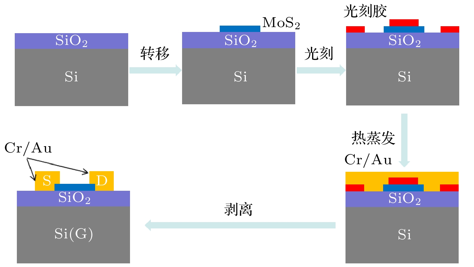
图 2 多层MoS2记忆晶体管的制备过程示意图
Figure 2. Diagram of the preparation processes of multilayer MoS2 memtransistor.

图 3 (a) 多层MoS2的AFM图像; (b) 多层MoS2的拉曼光谱
Figure 3. (a) AFM image of multilayer MoS2 ; (b) Raman spectrum of multilayer MoS2.

图 4 在0 V栅压时多层MoS2记忆晶体管的阻变特性 (a) 5 V至–5 V源漏电压扫描下器件Id-Vds曲线(插图: 器件在源极和漏极交换测试前后的Ids-Vds曲线); (b) 连续125个循环中器件在Vds = 0.6 V时高低阻态的阻值变化; (c)器件在室温下高低阻态保持特性图
Figure 4. Resistance characteristics of multilayer MoS2 memtransistor at Vg = 0 V: (a) Id-Vds characteristic of the device at cyclic sweeping of the Vds from 5 to –5 V (Inset: the Ids-Vds curves of the device before and after the source-drain electrode is exchanged); (b) the resistances of the device in high and low resistance states at Vds = 0.6 V during 125 cycles; (c) switching retention characteristics of the device at room temperature.
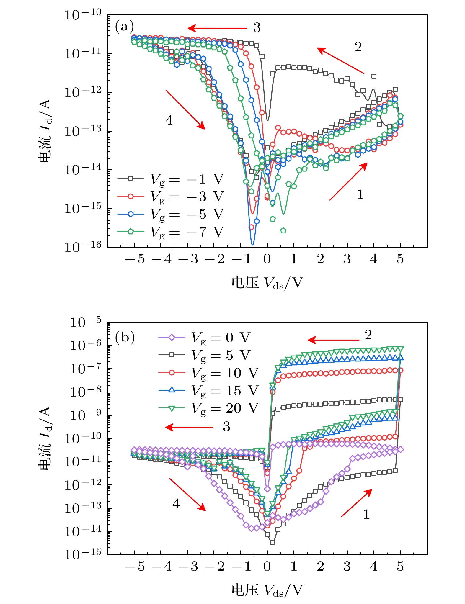
图 5 不同栅压下多层MoS2记忆晶体管的阻变特性 (a) 栅压Vg = –1, –3, –5, –7 V时的Id-Vds曲线; (b) 栅压Vg = 0, 5, 10, 15, 20 V时的Id-Vds曲线
Figure 5. Resistance characteristics of multilayer MoS2 memtransistor under different gate voltages: (a) Id-Vds characteristics of the device at Vg = –1, –3, –5, –7 V; (b) Id-Vds characteristics of the device at Vg = 0, 5, 10, 15, 20 V.

图 6 光场调控多层MoS2记忆晶体管的阻变特性 (a) 不同波长光照射时器件的Id-Vds曲线; (b) 不同波长光照射时器件的高低阻态阻值及开关比的变化
Figure 6. Resistance characteristics of multilayer MoS2 memtransistor under the control of the light field: (a) Id-Vds characteristics of the device under different wavelength illumination; (b) the resistances of the device in high and low resistance states and the corresponding ON/OFF radio under different wavelength illumination.

图 7 波长为200 , 400和800 nm光照射时, 器件高低阻态的阻值随栅压的变化(a)和电阻开关比随栅压的变化(b)
Figure 7. For incident light with 200, 400 and 800 nm wavelengths, (a) the resistances of the device versus Vg in high and low resistance states and (b) the ON/OFF radio versus Vg.

图 8 不同器件之间的性能对比 (a) 器件在不同栅压下开关比的变化; (b) 器件在不同波长下开关比的变化; (c) 器件在200, 400 和800 nm光照射时, 开关比随栅压的变化
Figure 8. Performance comparison between different devices: (a) Switching ratio of the devices under different gate voltages; (b) switching ratio of devices at different wavelengths; (c) switching ratio varies with gate voltages at illumination wavelengths of 200, 400 and 800 nm.
表 1 不同正栅压下器件的性能参数比较
Table 1. Performance parameters of the device at different forward gate voltages.
栅压 Vg/V 0 5 7 10 15 20 HRS阻值/Ω 1.82×10¹³ 2.85×10¹³ 7.40×10¹² 1.87×10¹² 4.46×10¹¹ 2.72×10¹¹ LRS阻值/Ω 1.08×10¹⁰ 2.78×10⁸ 4.74×10⁷ 1.25×10⁷ 4.42×10⁶ 2.95×10⁶ 开关比 1.69×10³ 1.03×10⁵ 1.56×10⁵ 1.50×10⁵ 1.01×10⁵ 0.92×10⁵  DownLoad: CSV
-
[1] Lu H, Seabaugh A 2014 IEEE J. Electron Devices Soc. 2 44
Google Scholar
[2] Sangwan V K, Lee H S, Bergeron H, Balla I, Beck M E, Chen K S, Hersam M C 2018 Nature 554 500
Google Scholar
[3] Yin S Q, Song C, Sun Y M, Qiao L L, Wang B L, Sun Y F, Liu K, Pan F, Zhang X Z 2019 ACS Appl. Mater. Interfaces 11 43344
Google Scholar
[4] Wang L, Liao W G, Wong S L, Yu Z G, Li S F, Lim Y F, Feng X W, Tan W C, Huang X, Chen L, Liu L, Chen J S, Gong X, Zhu C X, Liu X K, Zhang Y W, Chi D Z, Ang K W 2019 Adv. Funct. Mater. 29 1901106
Google Scholar
[5] Lee H S, Sangwan V K, Rojas W A G, Bergeron H, Jeong H Y, Yuan J T, Su K, Hersam M C 2020 Adv. Funct. Mater. 30 2003683
Google Scholar
[6] Yang Y, Du H Y, Xue Q, Wei X H, Yang Z B, Xu C G, Lin D M, Jie W J, Hao J H 2019 Nano Energy 57 566
Google Scholar
[7] Chen G L, Zhang L, Li L Y, Cheng F, Fu X, Li J H, Pan R K, Cao W Q, Chan A S, Panin G N, Wan J X, Zhang H, Liu C 2020 J. Alloys Compd. 823 153697
Google Scholar
[8] Park H, Mastro M A, Tadjer M J, Kim J 2019 Adv. Electron. Mater. 5 1900333
Google Scholar
[9] Zhao Y, Yu D Z, Liu Z, Li S J, He Z Y 2020 IEEE Access 8 106726
Google Scholar
[10] Dragoman M, Dinescu A, Nastase F, Dragoman D 2020 Nanomaterials 10 1404
Google Scholar
[11] Yu Y M, Yang F, Mao S S, Zhu S H, Jia Y F, Yuan L, Salmen M, Sun B 2018 Chem. Phys. Lett. 706 477
Google Scholar
[12] 余志强, 刘敏丽, 郎建勋, 钱楷, 张昌华 2018 物理学报 67 157302
Google Scholar
Yu Z Q, Liu M L, Lang J X, Qian K, Zhang C H 2018 Acta Phys. Sin. 67 157302
Google Scholar
[13] 孟凡一, 段书凯, 王丽丹, 胡小方, 董哲康 2015 物理学报 64 148501
Google Scholar
Meng F Y, Duan S K, Wang L D, Hu X F, Dong Z K 2015 Acta Phys. Sin. 64 148501
Google Scholar
[14] Dongale T D, Mohite S V, Bagade A A, Kamat R K, Rajpure K Y 2017 Microelectron. Eng. 183-184 12
[15] Rajkumari R, Singh N K 2020 ACS Appl. Nano Mater. 3 12087
Google Scholar
[16] Rodder M A, Vasishta S, Dodabalapur A 2020 ACS Appl. Mater. Interfaces 12 33926
Google Scholar
[17] Xu L P, Duan Z H, Zhang P, Wang X, Zhang J Z, Shang L Y, Jiang K, Li Y W, Zhu L Q, Gong Y J, Hu Z G, Chu J H 2020 ACS Appl. Mater. Interfaces 12 44902
Google Scholar
[18] Zhang S Q, Liu Y, Zhou J R, Ma M, Gao A Y, Zheng B J, Li L F, Su X, Han G Q, Zhang J C, Shi Y, Wang X M, Hao Y 2020 Nanoscale Res. Lett. 15 157
Google Scholar
[19] Wang Y H, Li D Y, Lai X B, Liu B Y, Chen Y B, Wang F P, Wang R M, Zhang L W 2020 Curr. Appl. Phys. 20 298
Google Scholar
[20] Ahmed Z, Shi Q, Ma Z C, Zhang L N, Guo H, Chan M S 2020 IEEE Electron Device Lett. 41 171
Google Scholar
[21] Huang X N, Yao Y, Peng S G, Zhang D Y, Shi J Y, Jin Z 2020 Materials 13 2896
Google Scholar
[22] Nalwa H S 2020 RCS Adv. 10 30529
Google Scholar
[23] 孙真昊, 管鸿明, 付雷, 沈波, 唐宁 2021 物理学报 70 027302
Sun Z H, Guan H M, Fu L, Shen B, Tang N 2021 Acta Phys. Sin. 70 027302
[24] Bao W Z, Cai X H, Kim D, Sridhara K, Fuhrer M S 2013 Appl. Phys. Lett. 102 042104
Google Scholar
[25] Zhang J, Yu H, Chen W, Tian X Z, Liu D H, Cheng M, Xie G B, Yang W, Yang R, Bai X D, Shi D X, Zhang G Y 2014 ACS Nano 8 6024
Google Scholar
[26] Yu H, Liao M Z, Zhao W J, Liu G D, Zhou X J, Wei Z, Xu X Z, Liu K H, Hu Z H, Deng K, Zhou S Y, Shi J A, Gu L, Shen C, Zhang T T, Du L J, Xie L, Zhu J Q, Chen W, Yang R, Shi D X, Zhang G Y 2017 ACS Nano 11 12001
Google Scholar
[27] Li D, Wu B, Zhu X J, Wang J T, Ryu B, Lu W D, Lu W, Liang X G 2018 ACS Nano 12 9240
Google Scholar
[28] Kim K S, Ji Y J, Kim K H, Choi S, Kang D H, Heo K, Cho S, Yim S, Lee S, Park J H, Jung Y S, Yeom G Y 2019 Nat. Commun. 10 4701
Google Scholar

 DownLoad:
Catalog
Metrics
- Abstract views: 4547
- PDF Downloads: 172
- Cited By: 0
