


-
Memtransistor is a multiterminal device combining the concepts of memristor and field-effect transistor. Two-dimensional transition metal sulfides have unique electronic structure and properties, and they are widely used in electronic devices, energy conversions, memories and other fields. In this work, a two-dimensional ReSe2/WSe2 heterostructure memtransistor is prepared, then the resistive switching characteristics under the electrical modulation, optical modulation, and electric-optical dual gate control are discussed. The results show that the gate control is an effective modulation method, which can change the on/off ratio of the device from 101 to 105. Then, the resistance and on/off ratio of the memtransistor can be controlled by changing the light wavelength and the illumination power. Moreover, the switching ratio of the device can also be changed in a range of 102–105 by electric and light dual-gate control, and the reasons for the change of resistance states of the device under different modulation conditions are analyzed. Furthermore, after 225 cycles and 1.9 × 10⁴ s, the ReSe2/WSe2 heterostructure memtransistor still maintains a switch ratio close to 104, indicating the good stability and durability of the device. It demonstrates that the ReSe2/WSe2 memtransistor will be one of potential candidates for the next- generation nonvolatile memory applications.
-
Keywords:
- ReSe2/WSe2 /
- memtransistor /
- gate control /
- optical control
[1] Chua L 1971 IEEE Trans. Circuit Theory 5 507
 Google Scholar
[2] Strukov D B, Snider G S, Stewart D R, Williams R S 2008 Nature 453 80
Google Scholar
[3] Cheng S L, Fan Z, Rao J J, Hong L Q, Huang Q C, Tao R Q, Hou Z P, Qin M H, Zeng M, Lu X B, Zhou G F, Yuan G L, Gao X S, Liu J M 2020 Iscience 23 101874
Google Scholar
[4] Cui B Y, Fan Z, Li W J, Chen Y H, Dong S, Tan Z W, Cheng S L, Tian B B, Tao R Q, Tian G, Chen D Y, Hou Z P, Qin M H, Zeng M, Lu X B, Zhou G F, Gao X S, Liu J M 2022 Nat. Commun. 13 1707
Google Scholar
[5] Waser R, Dittmann R, Staikov G, Szot K 2009 Adv. Mater. 21 2632
Google Scholar
[6] Xu X W, Ding Y K, Hu S X B, Niemier M, Cong J, Hu Y, Shi Y Y 2018 Nat. Electron. 1 216
Google Scholar
[7] Zeng M Q, Xiao Y, Liu J X, Yang K N, Fu L 2018 Chem. Rev. 118 6236
Google Scholar
[8] Nguyen D A, Oh H M, Duong N T, Bang S, Yoon S J, Jeong M S 2018 ACS Appl. Mater. Interfaces 10 10322
Google Scholar
[9] Shim J, Oh S, Kang D H, Jo S H, Ali M H, Choi W Y, Heo K, Jeon J, Lee S, Kim M, Song Y J, Park J H 2016 Nat. Commun. 7 13413
Google Scholar
[10] Yoshida M, Suzuki R, Zhang Y, Nakano M, Iwasa Y 2015 Sci. Adv. 1 e1500606
Google Scholar
[11] Vu Q A, Kim H, Nguyen V L, Won U Y, Adhikari S, Kim K, Lee Y H, Yu W J 2017 Adv. Mater. 29 1703363
Google Scholar
[12] Xu R J, Jang H, Lee M H, Amanov D, Cho Y, Kim H, Park S, Shin H J, Ham D 2019 Nano Lett. 19 2411
Google Scholar
[13] Park M, Park S, Yoo K H 2016 ACS Appl. Mater. Interfaces 8 14046
Google Scholar
[14] John R A, Liu F C, Chien N A, Kulkarni M R, Zhu C, Fu Q D, Basu A, Liu Z, Mathews N 2018 Adv. Mater. 30 1800220
Google Scholar
[15] Sangwan V K, Lee H S, Bergeron H, Beck M E, Chen K S, Hersam M C, Balla I 2018 Nature 554 500
Google Scholar
[16] Zhong Y N, Gao X, Xu J L, Siringhaus H, Wang S D 2020 Adv. Electron. Mater. 6 1900955
Google Scholar
[17] 邓文, 汪礼胜, 刘嘉宁, 余雪玲, 陈凤翔 2021 物理学报 70 217302
Google Scholar
Deng W, Wang L S, Liu J N, Yu X L, Chen F X 2021 Acta Phys. Sin. 70 217302
Google Scholar
[18] Zhang W G, Gao H, Deng C S, Lü T, Hu S H, Hao W, Xue S Y, Tao Y F, Deng L M, Xiong W 2021 Nanoscale 13 11497
Google Scholar
[19] Kim M, Ge R J, Wu X H, Lan X, Tice J, Lee J C, Akinwande D 2018 Nat. Commun. 9 2524
Google Scholar
[20] Rehman S, Kim H, Khan M F, Hur J H, Eom J, Kim D K 2021 J. Alloys Compd. 855 157310
Google Scholar
[21] 殷俊 2019 硕士学位论文 (北京: 清华大学)
Yin J 2019 M. S. Thesis (Beijing: Tsing University) (in Chinese)
[22] Tian X, Liu Y 2021 J. Semicond. 42 032001
Google Scholar
[23] Zhou X, Hu X Z, Zhou S S, Song H Y, Zhang Q, Pi L J, Li L, Li H Q, Lü J T, Zhai T Y 2018 Adv. Mater. 30 1703286
Google Scholar
[24] Ali M H, Kang D H, Park J H 2017 Org. Electron. 53 14
[25] Li D, Wu B, Zhu X J, Wang J T, Ryu B, Lu W D, Liang X G 2018 ACS Nano 12 9240
Google Scholar
[26] Wang L, Liao W G, Wong S L, Yu Z G, Li S F, Lim Y F, Feng X W, Tan W C, Huang X, Chen L, Liu L, Chen J S, Gong X, Zhu C X, Liu X K, Zhang Y W, Chi D Z, Ang K W 2019 Adv. Funct. Mater. 29 1901106
Google Scholar
[27] Wang C, Yang S, Xiong W Q, Xia C X, Cai H, Chen B, Wang X T, Zhang X Z, Wei Z M, Tongay S, Li J B, Liu Q 2016 Phys. Chem. Chem. Phys. 18 27750
Google Scholar
[28] Wang X T, Huang L, Peng Y T, Huo N J, Wu K D, Xia C X, Wei Z M, Tongay S, Li J B 2016 Nano Res. 9 507
Google Scholar
[29] Ahn J, Ko K, Kyhm J H, Ra H S, Bae H, Hong S, Kim D Y, Jang J, Kim T W, Choi S, Kang J H, Kwon N, Park S, Ju B K, Poon T C, Park M C, Im S, Hwang D K 2021 ACS Nano 15 17917
Google Scholar
[30] Yang Y C, Gao P, Gaba S, Chang T, Pan X Q, Lu W 2012 Nat. Commun. 3 732
Google Scholar
[31] Jang M H, Agarwal R, Nukala P, Choi D, Johson A T C, Chen I W, Agarwal R 2016 Nano Lett. 16 2139
Google Scholar
[32] 田学伟, 王永生, 张璐, 刘安琪, 何大伟 2018 中国科技信息 13 98
Google Scholar
Tian X W, Wang Y S, Zhang L, Liu A Q, He D W 2018 Chin. Sci. Technol. Inf. 13 98
Google Scholar
[33] Yin S Q, Song C, Sun Y M, Qiao L L, Wang B L, Sun Y F, Liu K, Pan F, Zhang X Z 2019 ACS Appl. Mater. Interfaces 11 43344
Google Scholar
[34] 张璐 2016 硕士学位论文 (北京: 北京交通大学)
Zhang L 2016 M. S. Thesis (Beijing: Beijing Jiaotong University) (in Chinese)
[35] 夏风梁, 石凯熙, 赵东旭, 王云鹏, 范翊, 李金华 2021 发光学报 42 257
Google Scholar
Xia F L, Shi K X, Zhao D X, Wang Y P, Fan Y, Li J H 2021 Chin. J. Lumin. 42 257
Google Scholar
-
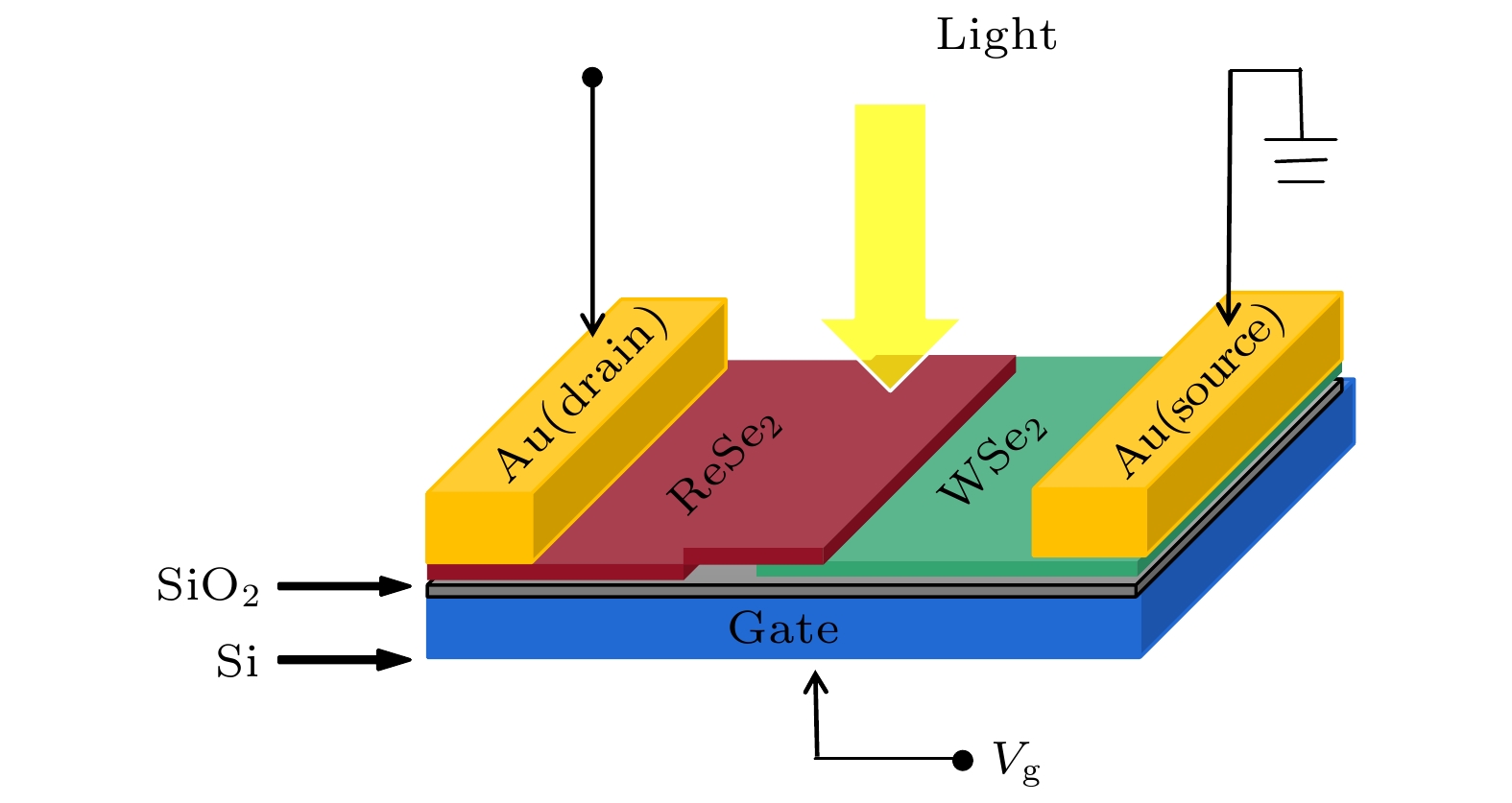
图 1 ReSe2/WSe2异质结晶体管的结构图
Figure 1. Structure diagram of the ReSe2/WSe2 heterojunction memtransistor
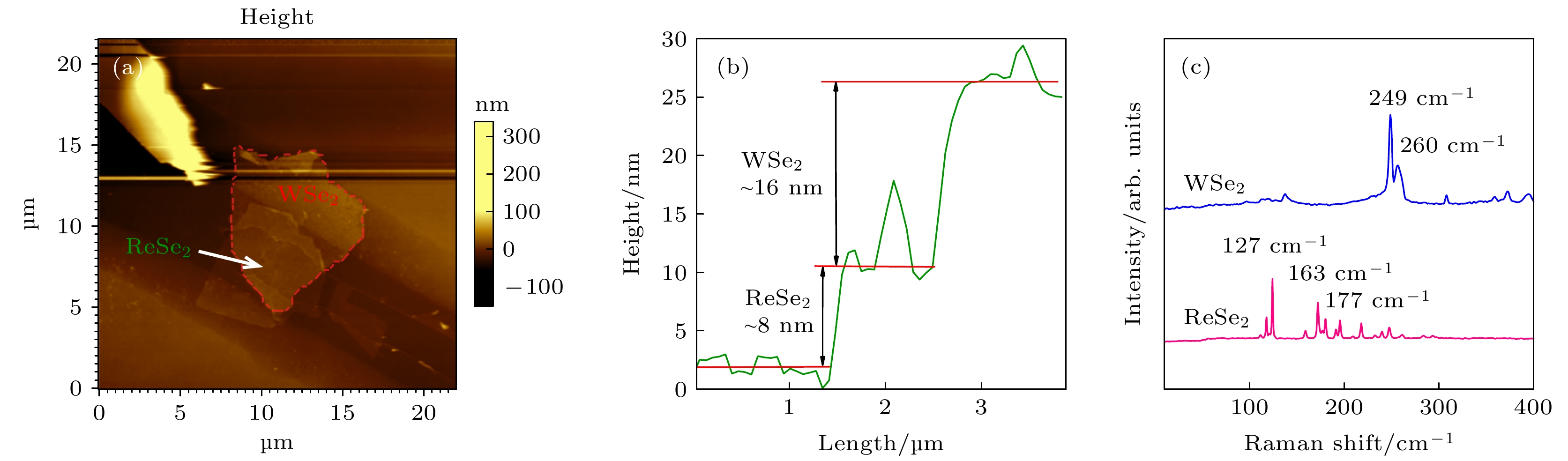
图 2 ReSe2/WSe2异质结的形貌表征 (a) ReSe2/WSe2异质结的AFM图; (b) 沿图(a)中白色箭头的厚度数据图; (c) WSe2和ReSe2的拉曼光谱图
Figure 2. Surface topography image of ReSe2/WSe2 heterojunction memtransistor: (a) AFM image of ReSe2/WSe2 heterojunction; (b) height profile of ReSe2/WSe2 along the thin white line in panel (a); (c) Raman spectra of the WSe2 and ReSe2 layer
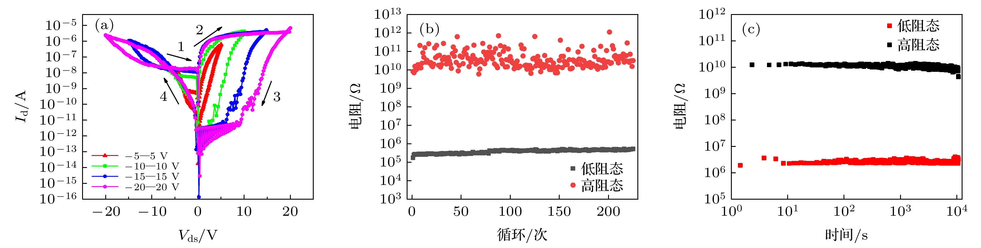
图 3 在0 V栅压下, Au/ReSe2/WSe2/Au记忆晶体管的阻变特性 (a) 在不同源漏扫描电压下的Id-Vds特性曲线; (b) 连续225次循环周期下器件在Vds = 2.4 V时的高低阻值变化图; (c) 器件在室温下高低阻态保持特性图
Figure 3. Resistance characteristics of the Au/ReSe2/WSe2/Au memtransistor at Vg = 0 V: (a) Id-Vds characteristic curves of Au/ReSe2/WSe2/Au memtransistor at different source drain sweeping voltages; (b) reversible resistance switching between the HRS and LRS over 225 cycles at Vds = 2.4 V; (c) the retention characteristics of the device at room temperature

图 4 ReSe2/WSe2记忆晶体管的阻变转换机制分析 (a) ReSe2和WSe2单独的能带图; (b) ReSe2/WSe2异质结的平衡能带图; (c) 负偏置电压下的双对数Id-Vds曲线
Figure 4. Resistance switching mechanism analysis of ReSe2/WSe2 memtransistor: (a) Energy band arrangement for ReSe2 and WSe2; (b) energy band diagram of ReSe2/WSe2 heterojunction; (c) logarithmic Id-Vds curves of the memtransistor in the negative bias region

图 5 在–1 V < Vg < 1 V范围中, 不同栅压下ReSe2/WSe2记忆晶体管的阻变特性 (a) 负栅压Vg = –0.1— –1 V时的Id-Vds特性曲线; (b) 正栅压Vg = 0.1—1 V时的Id-Vds特性曲线(0 V作为参考)
Figure 5. Resistance characteristics of ReSe2/WSe2 memtransistors at different gate voltages in the range of –1 V < Vg < 1 V: (a) Id-Vds characteristic curves at negative gate voltage Vg = –0.1−–1 V; (b) Id-Vds characteristic curves at positive gate voltage Vg = 0.1−1 V (the black line with Vg = 0 V is as a reference)
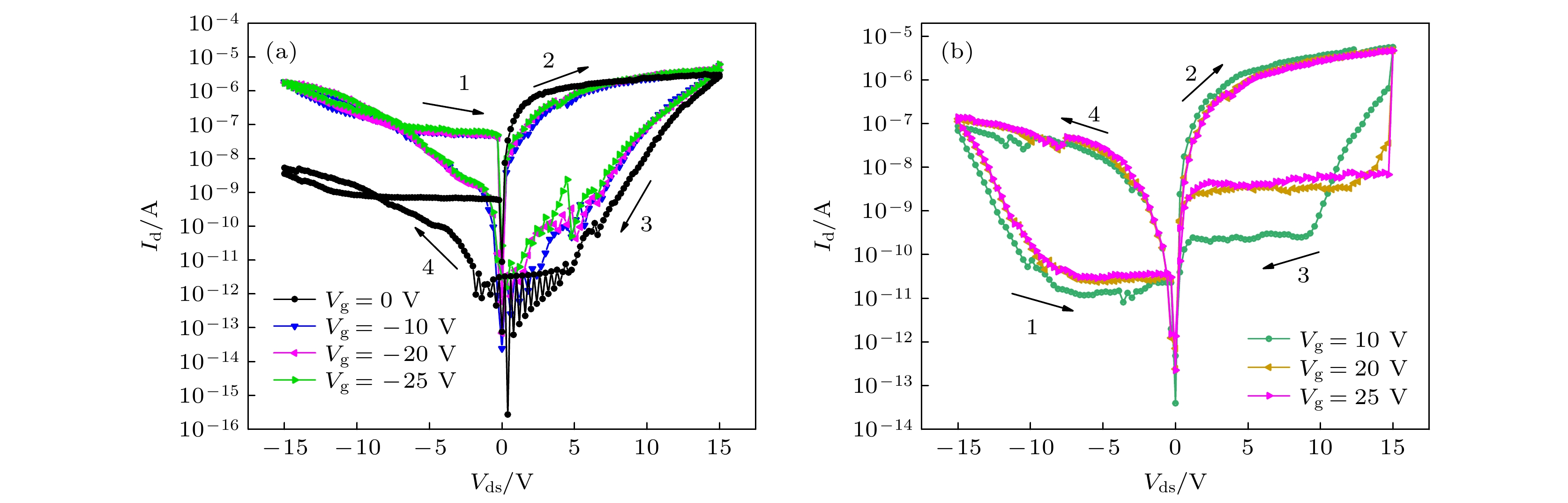
图 6 高栅压(|Vg| > 10 V)时, 不同栅压下Au/ReSe2/WSe2/Au器件的阻变特性 (a) 负栅压Vg = –10—–25 V时的Id-Vds特性曲线(其中0 V曲线作为参考); (b) 正栅压Vg = 10—25 V时的Id-Vds特性曲线
Figure 6. Resistance characteristics of Au/ReSe2/WSe2/Au device at higher gate voltages (|Vg| > 10 V): (a) Id-Vds characteristic curves at negative gate voltages Vg = –10−–25 V (the black line with Vg = 0 V is as a reference) ; (b) Id-Vds characteristic curves at positive gate voltages Vg = 10−25 V
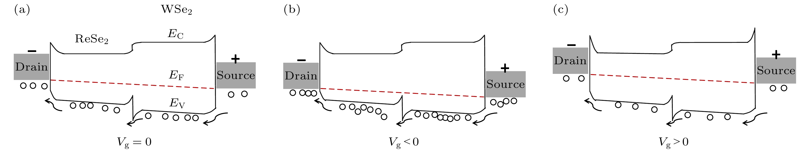
图 7 Au/ReSe2/WSe2/Au记忆晶体管的简化能带图(Vds < 0) (a) Vg = 0 V; (b) Vg < 0 V; (c) Vg > 0 V
Figure 7. Simplified band diagram of Au/ReSe2/WSe2/Au memtransistor (Vds < 0): (a) Vg = 0 V; (b) Vg < 0 V; (c) Vg > 0 V
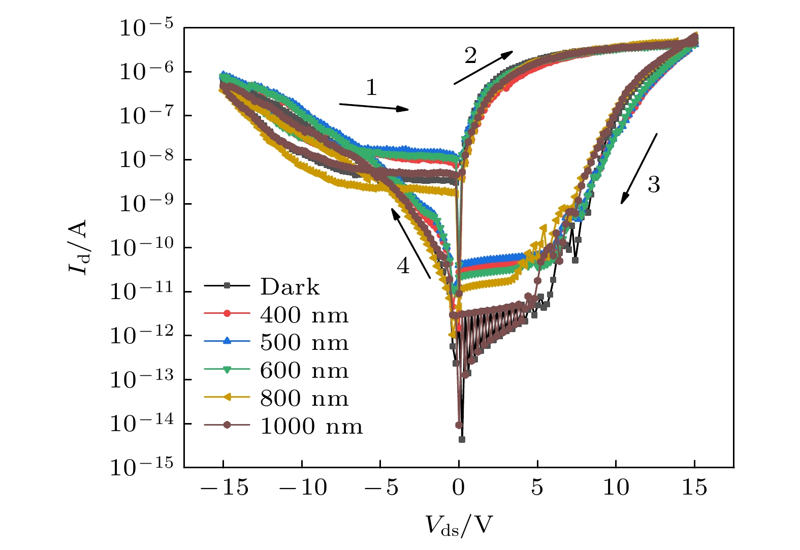
图 8 Au/ReSe2/WSe2/Au器件在不同波长光栅调控下的Id-Vds曲线
Figure 8. Id-Vds curves of the Au/ReSe2/WSe2/Au device under optical modulation with different wavelengths
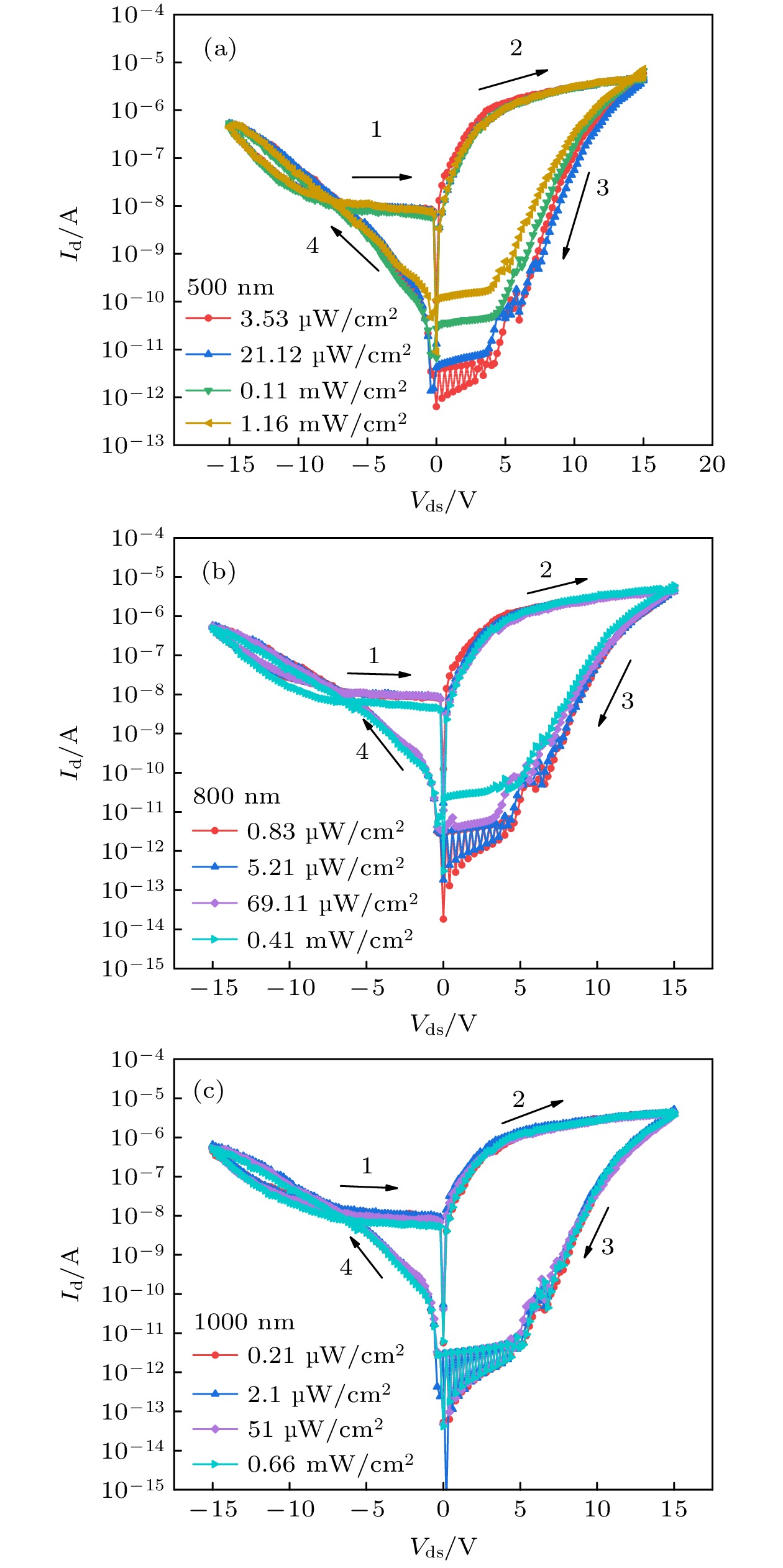
图 9 不同波长、不同光强下器件的Id-Vds特性曲线 (a) 500 nm光照; (b) 800 nm光照; (c) 1000 nm光照
Figure 9. Id-Vds curves of the device under different wavelengths and powers: (a) 500 nm illumination; (b) 800 nm illumination; (c) 1000 nm illumination
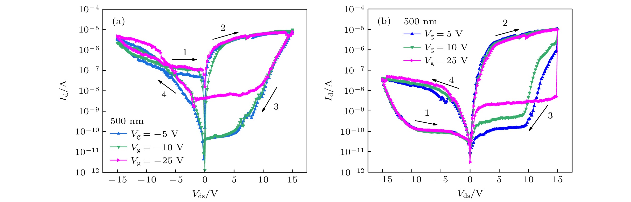
图 10 500 nm波长光照和电场同时调控下器件的阻变特性 (a) 负栅压Vg = –5—25 V时的Id-Vds曲线; (b) 正栅压Vg = 5—25 V时的Id-Vds曲线
Figure 10. Resistance characteristics of electric and light dual-gate tunable memtransistor with illumination wavelength of 500 nm: (a) Id-Vds curves at negative gate voltages Vg = –5–25 V; (b) Id-Vds curves at positive gate voltages Vg = 5–25 V
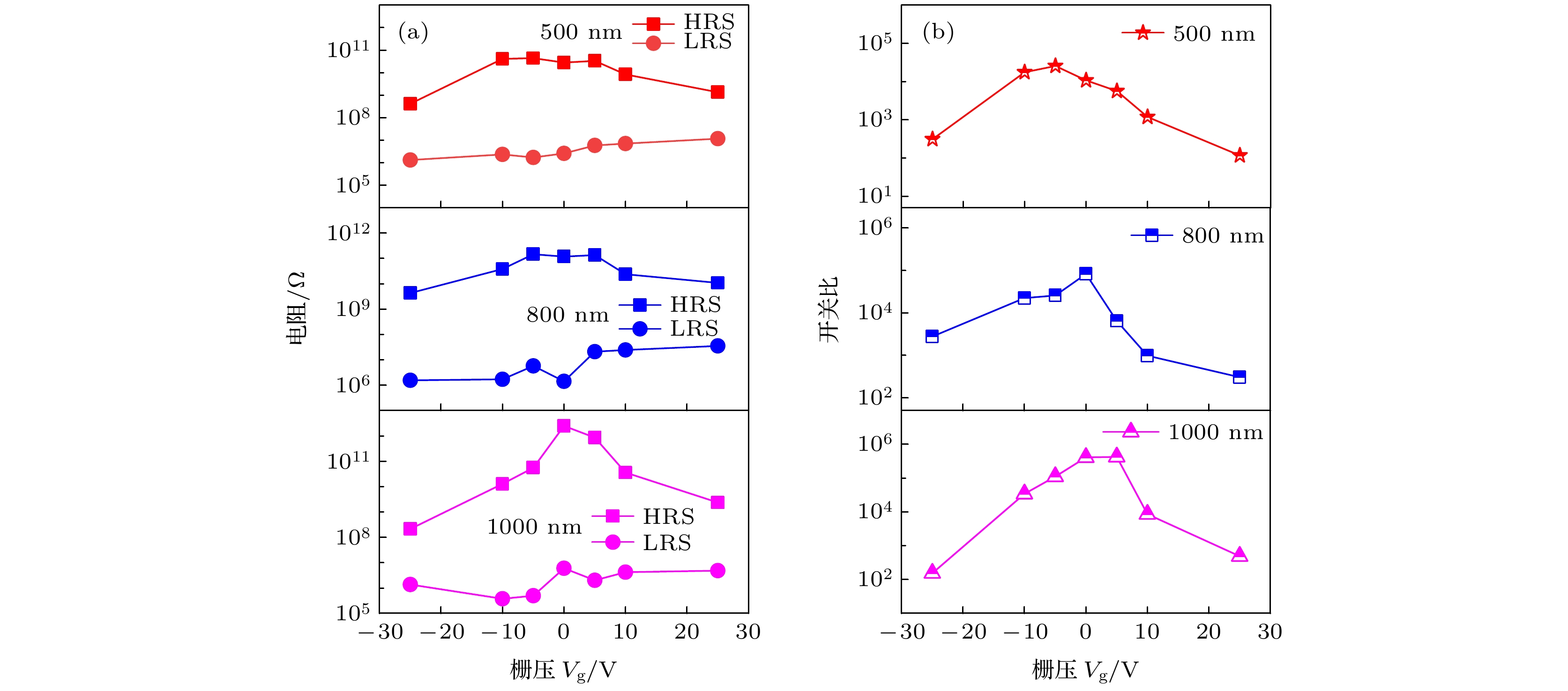
图 11 光场和电场的双栅协控下, Au/ReSe2/WSe2/Au记忆晶体管特性 (a) 器件的高低阻态随栅压、波长的变化; (b) 开关比随栅压、波长的变化
Figure 11. Electric and light dual-gate tunable Au/ReSe2/WSe2/Au memtransistor: (a) The high and low resistance states of the devices under different gate voltages and different incident wavelengths; (b) on/off ratio of the devices under different gate voltages and different incident wavelengths.
表 1 不同正栅压下器件的详细参数
Table 1. Detailed parameters of the device under different positive gate voltages
栅压 Vg/V 0 1 10 20 25 HRS阻
值/Ω6.31 ×
10114.36 ×
10111.20 ×
10108.75 ×
1085.26 ×
108LRS阻
值/Ω2.37 ×
1064.31 ×
1065.59 ×
1069.66 ×
1061.12 ×
107开关比 2.66 ×
1051.01 ×
1052.14 ×
1039.06 ×
1014.70 ×
101 DownLoad: CSV
-
[1] Chua L 1971 IEEE Trans. Circuit Theory 5 507
Google Scholar
[2] Strukov D B, Snider G S, Stewart D R, Williams R S 2008 Nature 453 80
Google Scholar
[3] Cheng S L, Fan Z, Rao J J, Hong L Q, Huang Q C, Tao R Q, Hou Z P, Qin M H, Zeng M, Lu X B, Zhou G F, Yuan G L, Gao X S, Liu J M 2020 Iscience 23 101874
Google Scholar
[4] Cui B Y, Fan Z, Li W J, Chen Y H, Dong S, Tan Z W, Cheng S L, Tian B B, Tao R Q, Tian G, Chen D Y, Hou Z P, Qin M H, Zeng M, Lu X B, Zhou G F, Gao X S, Liu J M 2022 Nat. Commun. 13 1707
Google Scholar
[5] Waser R, Dittmann R, Staikov G, Szot K 2009 Adv. Mater. 21 2632
Google Scholar
[6] Xu X W, Ding Y K, Hu S X B, Niemier M, Cong J, Hu Y, Shi Y Y 2018 Nat. Electron. 1 216
Google Scholar
[7] Zeng M Q, Xiao Y, Liu J X, Yang K N, Fu L 2018 Chem. Rev. 118 6236
Google Scholar
[8] Nguyen D A, Oh H M, Duong N T, Bang S, Yoon S J, Jeong M S 2018 ACS Appl. Mater. Interfaces 10 10322
Google Scholar
[9] Shim J, Oh S, Kang D H, Jo S H, Ali M H, Choi W Y, Heo K, Jeon J, Lee S, Kim M, Song Y J, Park J H 2016 Nat. Commun. 7 13413
Google Scholar
[10] Yoshida M, Suzuki R, Zhang Y, Nakano M, Iwasa Y 2015 Sci. Adv. 1 e1500606
Google Scholar
[11] Vu Q A, Kim H, Nguyen V L, Won U Y, Adhikari S, Kim K, Lee Y H, Yu W J 2017 Adv. Mater. 29 1703363
Google Scholar
[12] Xu R J, Jang H, Lee M H, Amanov D, Cho Y, Kim H, Park S, Shin H J, Ham D 2019 Nano Lett. 19 2411
Google Scholar
[13] Park M, Park S, Yoo K H 2016 ACS Appl. Mater. Interfaces 8 14046
Google Scholar
[14] John R A, Liu F C, Chien N A, Kulkarni M R, Zhu C, Fu Q D, Basu A, Liu Z, Mathews N 2018 Adv. Mater. 30 1800220
Google Scholar
[15] Sangwan V K, Lee H S, Bergeron H, Beck M E, Chen K S, Hersam M C, Balla I 2018 Nature 554 500
Google Scholar
[16] Zhong Y N, Gao X, Xu J L, Siringhaus H, Wang S D 2020 Adv. Electron. Mater. 6 1900955
Google Scholar
[17] 邓文, 汪礼胜, 刘嘉宁, 余雪玲, 陈凤翔 2021 物理学报 70 217302
Google Scholar
Deng W, Wang L S, Liu J N, Yu X L, Chen F X 2021 Acta Phys. Sin. 70 217302
Google Scholar
[18] Zhang W G, Gao H, Deng C S, Lü T, Hu S H, Hao W, Xue S Y, Tao Y F, Deng L M, Xiong W 2021 Nanoscale 13 11497
Google Scholar
[19] Kim M, Ge R J, Wu X H, Lan X, Tice J, Lee J C, Akinwande D 2018 Nat. Commun. 9 2524
Google Scholar
[20] Rehman S, Kim H, Khan M F, Hur J H, Eom J, Kim D K 2021 J. Alloys Compd. 855 157310
Google Scholar
[21] 殷俊 2019 硕士学位论文 (北京: 清华大学)
Yin J 2019 M. S. Thesis (Beijing: Tsing University) (in Chinese)
[22] Tian X, Liu Y 2021 J. Semicond. 42 032001
Google Scholar
[23] Zhou X, Hu X Z, Zhou S S, Song H Y, Zhang Q, Pi L J, Li L, Li H Q, Lü J T, Zhai T Y 2018 Adv. Mater. 30 1703286
Google Scholar
[24] Ali M H, Kang D H, Park J H 2017 Org. Electron. 53 14
[25] Li D, Wu B, Zhu X J, Wang J T, Ryu B, Lu W D, Liang X G 2018 ACS Nano 12 9240
Google Scholar
[26] Wang L, Liao W G, Wong S L, Yu Z G, Li S F, Lim Y F, Feng X W, Tan W C, Huang X, Chen L, Liu L, Chen J S, Gong X, Zhu C X, Liu X K, Zhang Y W, Chi D Z, Ang K W 2019 Adv. Funct. Mater. 29 1901106
Google Scholar
[27] Wang C, Yang S, Xiong W Q, Xia C X, Cai H, Chen B, Wang X T, Zhang X Z, Wei Z M, Tongay S, Li J B, Liu Q 2016 Phys. Chem. Chem. Phys. 18 27750
Google Scholar
[28] Wang X T, Huang L, Peng Y T, Huo N J, Wu K D, Xia C X, Wei Z M, Tongay S, Li J B 2016 Nano Res. 9 507
Google Scholar
[29] Ahn J, Ko K, Kyhm J H, Ra H S, Bae H, Hong S, Kim D Y, Jang J, Kim T W, Choi S, Kang J H, Kwon N, Park S, Ju B K, Poon T C, Park M C, Im S, Hwang D K 2021 ACS Nano 15 17917
Google Scholar
[30] Yang Y C, Gao P, Gaba S, Chang T, Pan X Q, Lu W 2012 Nat. Commun. 3 732
Google Scholar
[31] Jang M H, Agarwal R, Nukala P, Choi D, Johson A T C, Chen I W, Agarwal R 2016 Nano Lett. 16 2139
Google Scholar
[32] 田学伟, 王永生, 张璐, 刘安琪, 何大伟 2018 中国科技信息 13 98
Google Scholar
Tian X W, Wang Y S, Zhang L, Liu A Q, He D W 2018 Chin. Sci. Technol. Inf. 13 98
Google Scholar
[33] Yin S Q, Song C, Sun Y M, Qiao L L, Wang B L, Sun Y F, Liu K, Pan F, Zhang X Z 2019 ACS Appl. Mater. Interfaces 11 43344
Google Scholar
[34] 张璐 2016 硕士学位论文 (北京: 北京交通大学)
Zhang L 2016 M. S. Thesis (Beijing: Beijing Jiaotong University) (in Chinese)
[35] 夏风梁, 石凯熙, 赵东旭, 王云鹏, 范翊, 李金华 2021 发光学报 42 257
Google Scholar
Xia F L, Shi K X, Zhao D X, Wang Y P, Fan Y, Li J H 2021 Chin. J. Lumin. 42 257
Google Scholar

 DownLoad:
Catalog
Metrics
- Abstract views: 2570
- PDF Downloads: 81
- Cited By: 0
