


-
The transistor is the core unit of digital integrated circuits, and its performance and integration are the main determinants of chip performance. With the continuous progress of nano-manufacturing technology and process, high power and heat consumption have become a major problem restricting the development of integrated circuits. Using topological insulators instead of traditional semiconductors, and the spin and valley degrees of freedom instead of charge as information carriers, to design and fabricate transistors, and the use of optical interconnections to replace metal interconnections between functional units, are effective solutions of the thermal power consumption problem of nano-integrated circuits. Based on the two-dimensional topological insulators-silicene and germanene, we theoretically propose a kind of optically controlled transistor suitable for spin bias. The effects of off-resonant circularly polarized light on the output currents of silicene and germanene transistors are calculated by using the non-equilibrium Green's function method. It is shown that the topological properties of silicene (germanene) and the output characteristics of drain current are controlled by the chirality and intensity of incident light. Under the coaction of weak left circularly polarized light and spin bias, the silicene transistors output pure spin current and fully polarized spin-up current. Under the action of strong field, the phase transition of the edge state of the silicene forms a band gap, the transistor is cut off, and the output current is almost zero. Different from the silicene transistor, the germanene transistor can obtain stable pure spin current under a weak light field, and output 100% polarized spin-down current under a strong field. By simultaneously applying off-resonant circularly polarized light of different chirality to the central device region, the germanene transistor can be turned off effectively by using the edge state phase transition induced by the polarized light field and the energy band mismatch caused by the local light field. The output poles of spin-dependent currents are almost equal for silicene and germanene transistors in the ON state, however, the breakdown voltage of the germanene transistor is significantly higher than that of the silicene transistor, and optically controlled germanene transistor can maintain effective operation at higher temperatures.
-
Keywords:
- optically controlled transistor /
- off-resonance circularly polarized light /
- topological insulator
[1] Takeda K, Shiraishi K 1994 Phys. Rev. B 50 1491
 Google Scholar
[2] Novoselov K S, Geim A K, Morozov S V, Jiang D, Zhang Y, Dubonos S V, Grigorieva I V, Firsov A A 2004 Science 306 666
Google Scholar
[3] Guzman-Verri G G, Lew-Yan-Voon L C 2007 Phys. Rev. B 76 075131
Google Scholar
[4] Cahangirov S, Topsakal M, Akturk E, Sahin H, Ciraci S 2009 Phys. Rev. Lett. 102 236804
Google Scholar
[5] Liu C C, Feng W X, Yao Y G 2011 Phys. Rev. Lett. 107 076802
Google Scholar
[6] Liu C C, Jiang H, Yao Y G 2011 Phys. Rev. B 84 195430
Google Scholar
[7] Ezawa M 2012 Phys. Rev. Lett. 109 055502
Google Scholar
[8] Chen L, Liu C C, Feng B J, He X Y, Cheng P, Ding Z J, Meng S, Yao Y G, Wu K H 2012 Phys. Rev. Lett. 109 056804
Google Scholar
[9] Vogt P, Padova P D, Quaresima C, Avila J, Frantzeskakis E, Asensio M C, Resta A, Ealet B, Le-Lay G 2012 Phys. Rev. Lett. 108 155501
Google Scholar
[10] Fleurence A, Friedlein R, Ozaki T, Kawai H, Wang Y, Yamada-Takamura Y 2012 Phys. Rev. Lett. 108 245501
Google Scholar
[11] Meng L, Wang Y L, Zhang L Z, Du S X, Wu R T, Li L F, Zhang Y, Li G, Zhou H T, Hofer W A, Gao H J 2013 Nano Lett. 13 685
Google Scholar
[12] Li L F, Lu S Z, Pan J B, Qin Z H, Wang Y Q, Wang Y L, Cao G Y, Du S X, Gao H J 2014 Adv. Mater. 26 4820
Google Scholar
[13] Davila M E, Xian L, Cahangirov S, Rubio A, Le-Lay G 2014 New J. Phys. 16 095002
Google Scholar
[14] Derivaz M, Dentel D, Stephan R, Hanf M C, Mehdaoui A, Sonnet P, Pirri C 2015 Nano Lett. 15 2510
Google Scholar
[15] Zhang L, Bampoulis P, van Houselt A, Zandvliet H J W 2015 Appl. Phys. Lett. 107 111605
Google Scholar
[16] 黎明, 黄如 2018 中国科学: 信息科学 48 963
Google Scholar
Li M, Huang R 2018 Sci. Sin. Inform. 48 963
Google Scholar
[17] Hasan M Z, Kane C L 2010 Rev. Mod. Phys. 82 3045
Google Scholar
[18] Qi X L, Zhang S C 2011 Rev. Mod. Phys. 83 1057
Google Scholar
[19] Ni Z Y, Liu Q H, Tang K C, Zheng J X, Zhou J, Qin R, Gao Z X, Yu D P, Lu J 2012 Nano Lett. 12 113
Google Scholar
[20] Ezawa M 2013 Appl. Phys. Lett. 102 172103
Google Scholar
[21] Kaneko S, Tsuchiya H, Kamakura Y, Mori N, Ogawa M 2014 Appl. Phys. Express 7 035102
Google Scholar
[22] Ni Z Y, Zhong H X, Jiang X H, Quhe R G, Luo G F, Wang Y Y, Ye M, Yang J B, Shi J J, Lu J 2014 Nanoscale 6 7609
Google Scholar
[23] Tao L, Cinquanta E, Chiappe D, Grazianetti C, Fanciulli M, Dubey M, Molle A, Akinwande D 2015 Nat. Nanotechnol. 10 227
Google Scholar
[24] Pan F, Wang Y, Jiang K, Ni Z, Ma J, Zheng J, Quhe R G, Shi J, Yang J, Chen C and Lu J 2015 Sci. Rep. 5 9075
Google Scholar
[25] Wang Y Y, Ni Z Y, Liu Q H, Quhe R G, Zheng J X, Ye M, Yu D P, Shi J J, Yang J B, Li J, Lu J 2015 Adv. Funct. Mater. 25 68
Google Scholar
[26] Mahmoudi M, Ahangari Z, Fathipour M 2016 Chin. Phys. B 25 018501
Google Scholar
[27] Zhao Y, AlMutairi A, Yoon Y 2017 IEEE Electron Device Lett. 38 1743
Google Scholar
[28] Lima M P, Fazzio A, da Silva A J R 2018 IEEE Electron Device Lett. 39 1258
Google Scholar
[29] Zheng J, Chi F, Guo Y 2018 Appl. Phys. Lett. 113 112404
Google Scholar
[30] Kharadi M A, Malik G F A, Shah K A, Khanday F A 2019 IEEE Trans. Electron Devices 66 4976
Google Scholar
[31] Poljak M 2020 IEEE Trans. Electron Devices 67 354
Google Scholar
[32] Zheng J, Xiang Y, Li C L, Yuan R Y, Chi F, Guo Y 2020 Phys. Rev. Appl. 14 034027
Google Scholar
[33] Zheng J, Xiang Y, Li C L, Yuan R Y, Chi F, Guo Y 2021 Phys. Rev. Appl. 16 024046
Google Scholar
[34] Eckardt A, Anisimovas E 2015 New J. Phys. 17 093039
Google Scholar
[35] Eckardt A, Hauke P, Soltan-Panahi P, Becker C, Sengstock K, Lewenstein M 2010 Europhys. Lett. 89 10010
Google Scholar
[36] Kane C L, Mele E J 2005 Phys. Rev. Lett. 95 146802
Google Scholar
[37] Ezawa M 2013 Phys. Rev. Lett. 110 026603
Google Scholar
[38] Meir Y, Wingreen N S 1992 Phys. Rev. Lett. 68 2512
Google Scholar
[39] Datta S 1995 Electronic Transport in Mesoscopic Systems (New York: Cambridge University Press) p103
[40] Lee D H, Joannopoulos J D 1981 Phys. Rev. B 23 4997
Google Scholar
[41] Sun Q F, Guo H, Wang J 2003 Phys. Rev. Lett. 90 258301
Google Scholar
[42] Wang D K, Sun Q F, Guo H 2004 Phys. Rev. B 69 205312
Google Scholar
-
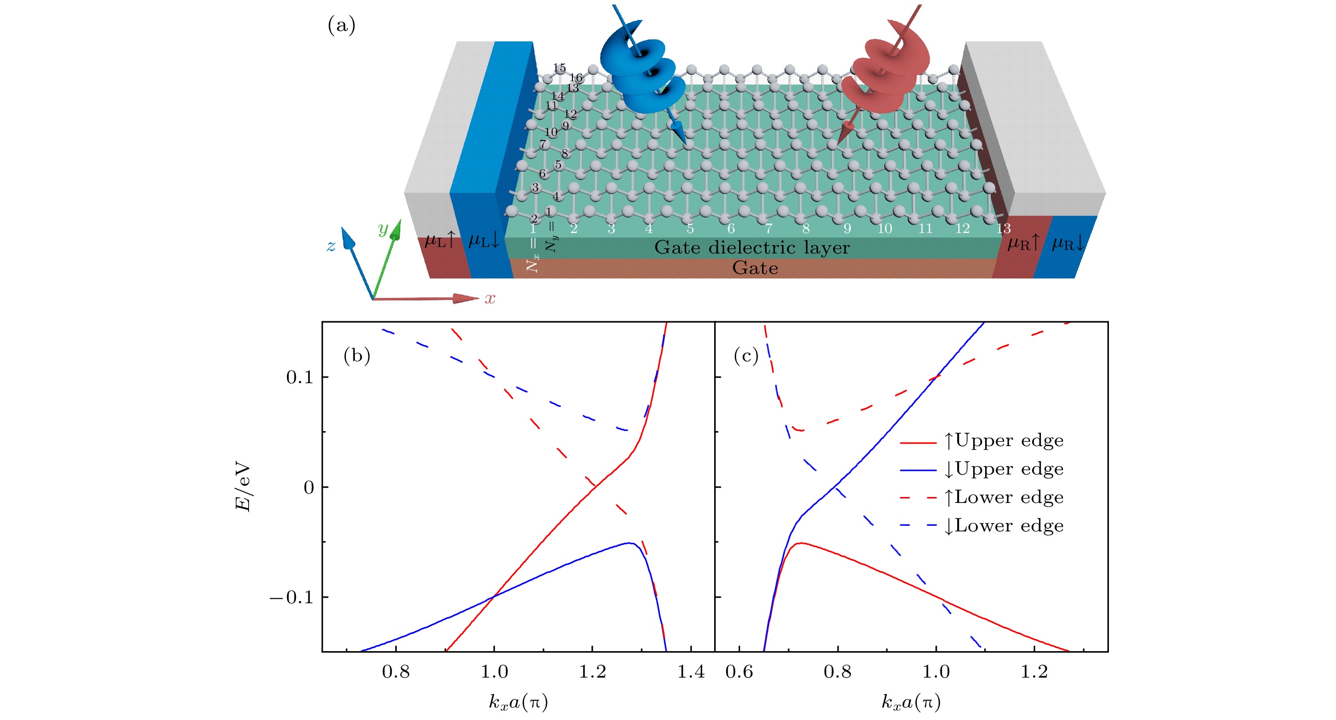
图 1 (a)自旋偏压驱动的硅(锗)烯光控晶体管结构示意图. 图中左旋圆偏振光和右旋圆偏振光同时照射器件中心区域, 硅(锗)烯层的下方是栅极电介质层和背栅极. 左右电极区域红色和蓝色长方体是自旋偏压产生的化学势示意图. (b)左旋圆偏振光场和电场共同作用时, 自旋向下边缘态相变后的锗烯能带图. (c) 右旋圆偏振光场作用下, 自旋向上边缘态相变后的锗烯能带图. 图(b)和图(c)的外场参数与图2(j)和图4(f)一致
Figure 1. (a) Schematic of a spin bias driven optically controlled silicene (germanene) transistor. In this figure, the left- and right-circularly polarized light illuminates simultaneously in the center of the device, and the gate dielectric layer and the back gate are below the silicene (germanene) sheet. The red and blue cuboids in the left and right electrode regions show the chemical potentials generated by the spin bias. (b) Energy band of germanene after the phase transition of the spin-down edge states under the joint action of the left-circularly polarized optical field and electric field. (c) Energy band diagram of germanene after the phase transition of the spin-up edge states under the effect of right-circularly polarized light. The field parameters of panels (b) and (c) are consistent with Fig. 2(j) and Fig. 4(f)
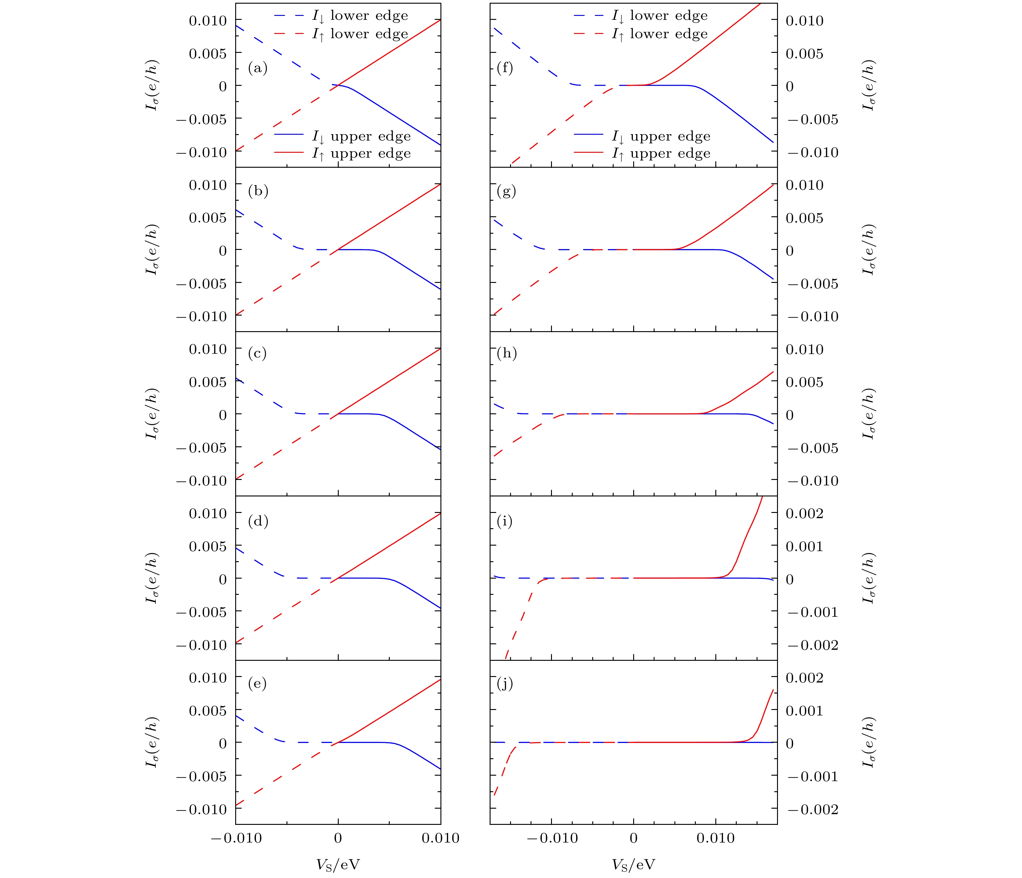
图 2 左旋圆偏振光场参数
$\lambda_{\varOmega}$ 和电场引起的交错势能$\lambda_{E}$ 取不同值时, 硅烯晶体管对外输出的自旋相关电流$I_\sigma$ 随自旋偏压$V_{\rm{S}}$ 的变化 (a) –0.002; (b) –0.004; (c) –0.006; (d) –0.008; (e) –0.01; (f) –0.02; (g) –0.04; (h) –0.06; (i) –0.08; (j) –0.1 eV. 图中红色和蓝色实线代表通过上边缘态输运的自旋向上和向下的电流, 虚线表示利用下边缘态输运的自旋相关的电流Figure 2. Spin dependent current
$I_\sigma$ as a function of the spin bias$V_{\rm{S}}$ when the left-circularly-polarized light parameter$\lambda_{\varOmega}$ and the electric field induced staggered potential$\lambda_{E}$ are chosen as: (a) –0.002; (b) –0.004; (c) –0.006; (d) –0.008; (e) –0.01; (f) –0.02; (g) –0.04; (h) –0.06; (i) –0.08; (j) –0.1 eV. The solid red and blue lines in the figures represent the spin-up and spin-down currents transported through the upper edge states, the dashed lines indicate the spin dependent currents using the lower edge states transport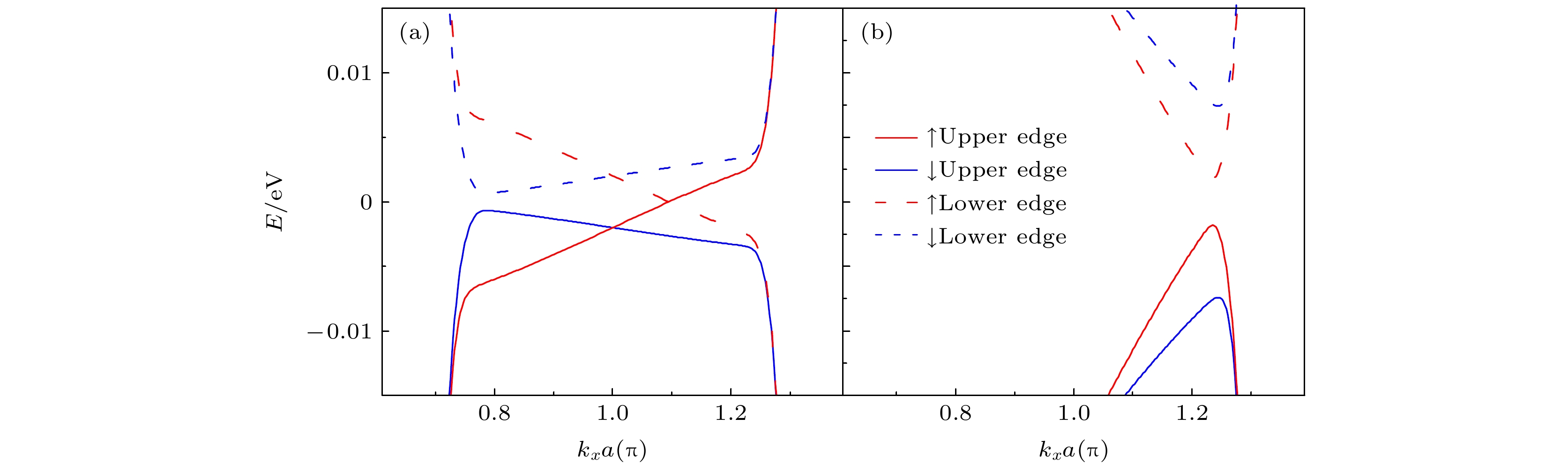
图 3 (a) 左旋圆偏振光场参数
$\lambda_{\varOmega}$ 和电场引起的交错势能$\lambda_{E}$ 为$\lambda_{\varOmega}=\lambda_{E}=-0.002$ eV时, 硅烯的边缘态能带结构; (b)$\lambda_{\varOmega}=\lambda_{E}=-0.02$ eV时, 硅烯的边缘态能带结构. 图中实线和虚线分别对应上边缘态和下边缘态, 红色和蓝色分别表示自旋向下和自旋向上电子形成的能带Figure 3. (a) Edge-states band structure of silicene when the left-circularly-polarized light parameter
$\lambda_{\varOmega}$ and the electric field induced staggered potential$\lambda_{E}$ are chosen as$\lambda_{\varOmega}=\lambda_{E}=-0.002$ eV; (b) Edge-states band structure of silicene when$\lambda_{\varOmega}=\lambda_{E}=-0.02$ eV. The solid and dashed lines correspond to the upper and lower edge states, and the red and blue lines indicate the energy bands formed by spin-down and spin-up electrons, respectively
图 4 对锗烯晶体管施加与图2相同强度的右旋圆偏振光场和电场时, 自旋相关电流
$I_\sigma$ 随自旋偏压$V_{\rm{S}}$ 的变化 (a)$\lambda_{\varOmega}=\lambda_{E} < $ $ 0.01$ ; (b)$\lambda_{\varOmega}=\lambda_{E}=0.02$ ; (c)$\lambda_{\varOmega}=\lambda_{E}=0.04$ ; (d)$\lambda_{\varOmega}=\lambda_{E}=0.06$ ; (e)$\lambda_{\varOmega}=\lambda_{E}=0.08$ ; (f)$\lambda_{\varOmega}=\lambda_{E}=0.1$ eV. 图中红色和蓝色实线代表通过上边缘态输运的自旋向上和向下的电流. 红色和蓝色虚线表示利用下边缘态输运的自旋向上和自旋向下的电流Figure 4. Variation of spin-dependent current
$I_\sigma$ with spin bias$V_{\rm{S}}$ when applying the same intensity of right-hand circularly polarized optical and electric fields to the germanene transistor as in Fig. 2: (a)$\lambda_{\varOmega}=\lambda_{E}<0.01$ ; (b)$\lambda_{\varOmega}=\lambda_{E}=0.02$ ; (c)$\lambda_{\varOmega}= $ $ \lambda_{E}=0.04$ ; (d)$\lambda_{\varOmega}=\lambda_{E}=0.06$ ; (e)$\lambda_{\varOmega}=\lambda_{E}=0.08$ ; (f)$\lambda_{\varOmega}=\lambda_{E}=0.1$ eV. The solid red and blue lines in the figures represent the spin-up and spin-down currents transported through the upper edge states. The red and blue dashed lines indicate the spin-up and spin-down currents using the lower edge states transport
图 5 对锗烯晶体管同时施加不同光参数的左旋和右旋圆偏振光时, 晶体管关态漏极电流
$I_\sigma$ 随自旋偏压$V_s$ 的变化 (a)$|\lambda_\varOmega|= $ $ 0.02$ ; (b)$|\lambda_\varOmega|=0.04$ ; (c)$|\lambda_\varOmega|=0.06$ ; (d)$|\lambda_\varOmega|=0.08$ ; (e)$|\lambda_\varOmega|= $ $ 0.1$ . 图中电场交错势能$\lambda_{E}=|\lambda_{\varOmega}|$ . 图中红色和蓝色实线代表通过上边缘态输运的自旋向上和向下的电流, 虚线表示利用下边缘态输运的自旋相关的电流Figure 5. Drain current of germanene transistor in the OFF state
$I_\sigma$ versus the spin bias$V_{\rm{S}}$ when the left and right circularly polarized light fields of (a)$|\lambda_\varOmega|=0.02$ 、(b)$|\lambda_\varOmega|=0.04$ 、(c)$|\lambda_\varOmega|=0.06$ 、(d)$|\lambda_\varOmega|=0.08$ 、(e)$|\lambda_\varOmega|=0.1$ are applied simultaneously to the germanene transistor. The solid (dash) red and blue lines in the figures represent the spin-up and spin-down currents transported through the upper (lower) edge states. -
[1] Takeda K, Shiraishi K 1994 Phys. Rev. B 50 1491
Google Scholar
[2] Novoselov K S, Geim A K, Morozov S V, Jiang D, Zhang Y, Dubonos S V, Grigorieva I V, Firsov A A 2004 Science 306 666
Google Scholar
[3] Guzman-Verri G G, Lew-Yan-Voon L C 2007 Phys. Rev. B 76 075131
Google Scholar
[4] Cahangirov S, Topsakal M, Akturk E, Sahin H, Ciraci S 2009 Phys. Rev. Lett. 102 236804
Google Scholar
[5] Liu C C, Feng W X, Yao Y G 2011 Phys. Rev. Lett. 107 076802
Google Scholar
[6] Liu C C, Jiang H, Yao Y G 2011 Phys. Rev. B 84 195430
Google Scholar
[7] Ezawa M 2012 Phys. Rev. Lett. 109 055502
Google Scholar
[8] Chen L, Liu C C, Feng B J, He X Y, Cheng P, Ding Z J, Meng S, Yao Y G, Wu K H 2012 Phys. Rev. Lett. 109 056804
Google Scholar
[9] Vogt P, Padova P D, Quaresima C, Avila J, Frantzeskakis E, Asensio M C, Resta A, Ealet B, Le-Lay G 2012 Phys. Rev. Lett. 108 155501
Google Scholar
[10] Fleurence A, Friedlein R, Ozaki T, Kawai H, Wang Y, Yamada-Takamura Y 2012 Phys. Rev. Lett. 108 245501
Google Scholar
[11] Meng L, Wang Y L, Zhang L Z, Du S X, Wu R T, Li L F, Zhang Y, Li G, Zhou H T, Hofer W A, Gao H J 2013 Nano Lett. 13 685
Google Scholar
[12] Li L F, Lu S Z, Pan J B, Qin Z H, Wang Y Q, Wang Y L, Cao G Y, Du S X, Gao H J 2014 Adv. Mater. 26 4820
Google Scholar
[13] Davila M E, Xian L, Cahangirov S, Rubio A, Le-Lay G 2014 New J. Phys. 16 095002
Google Scholar
[14] Derivaz M, Dentel D, Stephan R, Hanf M C, Mehdaoui A, Sonnet P, Pirri C 2015 Nano Lett. 15 2510
Google Scholar
[15] Zhang L, Bampoulis P, van Houselt A, Zandvliet H J W 2015 Appl. Phys. Lett. 107 111605
Google Scholar
[16] 黎明, 黄如 2018 中国科学: 信息科学 48 963
Google Scholar
Li M, Huang R 2018 Sci. Sin. Inform. 48 963
Google Scholar
[17] Hasan M Z, Kane C L 2010 Rev. Mod. Phys. 82 3045
Google Scholar
[18] Qi X L, Zhang S C 2011 Rev. Mod. Phys. 83 1057
Google Scholar
[19] Ni Z Y, Liu Q H, Tang K C, Zheng J X, Zhou J, Qin R, Gao Z X, Yu D P, Lu J 2012 Nano Lett. 12 113
Google Scholar
[20] Ezawa M 2013 Appl. Phys. Lett. 102 172103
Google Scholar
[21] Kaneko S, Tsuchiya H, Kamakura Y, Mori N, Ogawa M 2014 Appl. Phys. Express 7 035102
Google Scholar
[22] Ni Z Y, Zhong H X, Jiang X H, Quhe R G, Luo G F, Wang Y Y, Ye M, Yang J B, Shi J J, Lu J 2014 Nanoscale 6 7609
Google Scholar
[23] Tao L, Cinquanta E, Chiappe D, Grazianetti C, Fanciulli M, Dubey M, Molle A, Akinwande D 2015 Nat. Nanotechnol. 10 227
Google Scholar
[24] Pan F, Wang Y, Jiang K, Ni Z, Ma J, Zheng J, Quhe R G, Shi J, Yang J, Chen C and Lu J 2015 Sci. Rep. 5 9075
Google Scholar
[25] Wang Y Y, Ni Z Y, Liu Q H, Quhe R G, Zheng J X, Ye M, Yu D P, Shi J J, Yang J B, Li J, Lu J 2015 Adv. Funct. Mater. 25 68
Google Scholar
[26] Mahmoudi M, Ahangari Z, Fathipour M 2016 Chin. Phys. B 25 018501
Google Scholar
[27] Zhao Y, AlMutairi A, Yoon Y 2017 IEEE Electron Device Lett. 38 1743
Google Scholar
[28] Lima M P, Fazzio A, da Silva A J R 2018 IEEE Electron Device Lett. 39 1258
Google Scholar
[29] Zheng J, Chi F, Guo Y 2018 Appl. Phys. Lett. 113 112404
Google Scholar
[30] Kharadi M A, Malik G F A, Shah K A, Khanday F A 2019 IEEE Trans. Electron Devices 66 4976
Google Scholar
[31] Poljak M 2020 IEEE Trans. Electron Devices 67 354
Google Scholar
[32] Zheng J, Xiang Y, Li C L, Yuan R Y, Chi F, Guo Y 2020 Phys. Rev. Appl. 14 034027
Google Scholar
[33] Zheng J, Xiang Y, Li C L, Yuan R Y, Chi F, Guo Y 2021 Phys. Rev. Appl. 16 024046
Google Scholar
[34] Eckardt A, Anisimovas E 2015 New J. Phys. 17 093039
Google Scholar
[35] Eckardt A, Hauke P, Soltan-Panahi P, Becker C, Sengstock K, Lewenstein M 2010 Europhys. Lett. 89 10010
Google Scholar
[36] Kane C L, Mele E J 2005 Phys. Rev. Lett. 95 146802
Google Scholar
[37] Ezawa M 2013 Phys. Rev. Lett. 110 026603
Google Scholar
[38] Meir Y, Wingreen N S 1992 Phys. Rev. Lett. 68 2512
Google Scholar
[39] Datta S 1995 Electronic Transport in Mesoscopic Systems (New York: Cambridge University Press) p103
[40] Lee D H, Joannopoulos J D 1981 Phys. Rev. B 23 4997
Google Scholar
[41] Sun Q F, Guo H, Wang J 2003 Phys. Rev. Lett. 90 258301
Google Scholar
[42] Wang D K, Sun Q F, Guo H 2004 Phys. Rev. B 69 205312
Google Scholar

 DownLoad:


Catalog
Metrics
- Abstract views: 2175
- PDF Downloads: 61
- Cited By: 0
