


-
Stacking two or more monolayer materials to form van der Waals heterostructures is an effective strategy to realize ideal electronic and optoelectronic devices. In this work, we use As and HfS2 monolayers to construct As/Hfs2 heterostructures by six stacking manners, and from among them the most stable structure is selected to study its electronic and optic-electronic properties and quantum regulation effects by hybrid functional HSE06 systematically. It is found that the As/Hfs2 intrinsic heterostructure is a II-type band aligned semiconductor, and its band gap can be significantly reduced (~ 0.84 eV) in comparison with two monolayers (band gap > 2.0 eV), especially the valence band offset and conduction band offset can increase up to 1.48 eV and 1.31 eV, respectively, which is very favorable for developing high-performance optoelectronic devices and solar cells. The vertical strain can effectively adjust the band structure of heterostructure. The band gap increases by tensile strain, accompanied with an indirect-direct band gap transition. However, by compressive strain, the band gap decreases rapidly until the metal phase occurs. The applied external electric field can flexibly adjust the band gap and band alignment mode of heterostructure, so that the heterostructure can realize the transformation between I-, II-, and III-type band alignments. In addition, intrinsic As/Hfs2 heterostructure has ability to strongly absorb light in the visible light region, and can be further enhanced by external electric field and vertical strain. These results suggest that the intrinsic As/Hfs2 heterostructure promises to have potential applications in the fields of electronic, optoelectronic devices and photovoltaic cells.
-
Keywords:
- van der Waals heterostructure /
- II-type band alignment /
- vertical strain /
- external electric field /
- light adsorption coefficient
[1] Gupta A, Sakthivel T, Seal S 2015 Prog. Mater. Sci. 73 44
 Google Scholar
[2] Yang L, Chen W, Yu Q, Liu B 2021 Nano Res. 14 1583
Google Scholar
[3] Zhang R W, Zhang C W, Ji W X, Hu S J, Yan S S, Li S S, Li P, Wang P J, Liu Y S 2014 J. Phys. Chem. C 118 25278
Google Scholar
[4] Ni Z Y, Liu Q H, Tang K H, Zheng J X, Zhou J, Qin R, Gao Z X, Yu D P, Lu J 2012 Nano. Lett. 12 113
Google Scholar
[5] Massicotte M, Soavi G, Principi A, Tielrooij K J 2021 Nanoscale 13 8376
Google Scholar
[6] Blase X, Rubio A, Louie S G, Cohen M L, 1995 Phys. Rev. B 51 6868
Google Scholar
[7] Cahangirov S, Topsakal M, Aktürk E, Sahin H, Ciraci S 2009 Phys. Rev. Lett 102 236804
Google Scholar
[8] Kuang W, Hu R, Fan Z, Zhang Z 2019 Nanotechnology 30 145201
Google Scholar
[9] Xiao D, Liu G B, Feng W, Xu X, Yao W 2012 Phys. Rev. Lett 108 196802
Google Scholar
[10] Li X, Zhu H 2015 J. Materiomics 1 33
Google Scholar
[11] Yang G, Li L H, Lee W B, Ng M C 2018 Sci. Technol. Adv. Mater. 19 613
Google Scholar
[12] Low J, Yu J, Jaroniec M, Wageh S, Al‐Ghamdi A A 2017 Adv. Mater. 29 1601694
Google Scholar
[13] Wang H, Zhang L, Chen Z, Hu J Q, Li S J, Wang Z H, Liu J S, Wang X C 2014 Chem. Soc. Rev. 43 5234
Google Scholar
[14] Yan J A, Stein R, Schaefer D M, Wang X Q, Chou M Y 2013 Phys. Rev. B 88 121403
Google Scholar
[15] She L, Zhang F, Jia C, Kang L, Li Q, He X, Sun J, Lei Z, Liu Z 2021 Nanoscale 13 15781
Google Scholar
[16] He C, Zhang J H, Zhang W X, Li T T 2019 J. Phys. Chem. Lett. 10 3122
Google Scholar
[17] He C, Han F, Zhang W 2021 Chin. Chem. Lett. 33 404
[18] Li X, Li Z, Yang J 2014 Phys. Rev. Lett. 112 018301
Google Scholar
[19] Song W, Chen J, Li Z, Fang X 2021 Adv. Mater. 33 2101059
Google Scholar
[20] Chen F, Shi D, Yang M, Jiang H, Shao Y, Wang S, Zhang B, Shen J, Wu Y, Hao X 2021 Adv. Fun. Mater. 31 2007132
Google Scholar
[21] Peng D, Wang Y, Shi H, Wei J, Tao J, Zhao H, Chen Z 2022 J. Colloid Interface Sci. 613 194
Google Scholar
[22] Meitl M A, Zhu Z T, Kumar V, Lee K J, X. Feng, Huang Y Y, Adesida I, Nuzzo R G, Rogers J A 2006 Nat. Mater. 5 33
Google Scholar
[23] Castellanos-Gomez A, Buscema M, Molenaar R, Singh V, Janssen L, van der Zant H S J, Steele G A 2014 2D Mater. 1 011002
Google Scholar
[24] Gong Y, Lin J, Wang X, et al. 2014 Nat. Mater. 13 1135
Google Scholar
[25] Wang Y, Zhang C, Ji W, Wang P 2015 Appl. Phys. Express 8 065202
Google Scholar
[26] Kecik D, Durgun E, Ciraci S 2016 Phys. Rev. B 94 205410
Google Scholar
[27] Li Z J, Xu W, Yu Y Q, Du H Y, Zhen K, Wang J, Luo L B, Qiu H L, Yang X B, 2016 J. Mater. Chem. A 4 362
Google Scholar
[28] Xu C, Zhu M, Zheng H, Du X, Wang W, Yan Y 2016 RSC Adv. 6 43794
Google Scholar
[29] Sahin H, Sivek J, Li S, Partoens B, Peeters F M 2013 Phys. Rev. B 88 045434
Google Scholar
[30] Li Y, Xia C X, Wang T X, Tan X M, Zhao X, Wei S Y 2016 Solid State Commun. 230 6
Google Scholar
[31] Han J N, Zhang Z H, Fan Z Q, Zhou R L 2020 Nanotechnology 31 315206
Google Scholar
[32] Xie Z F, Sun F W, Yao R, Zhang Y, Zhang Y H, Zhang Z H, Fang Z B, Ni L, Duan L 2019 Appl. Surf. Sci. 475 839
Google Scholar
[33] Nie X R, Sun B Q, Zhu H, Zhang M, Zhao D H, Chen L, Sun Q Q, Zhang D W 2017 ACS Appl. Mater. Interfaces 9 26996
Google Scholar
[34] Kanazawa T, Amemiya T, Ishikawa A, Upadhyaya V, Tsuruta K, Tanaka T, Miyamoto Y 2016 Sci. Rep. 6 1
Google Scholar
[35] Fu L, Wang F, Wu B, Huang W 2017 Adv. Mater. 29 1700439
Google Scholar
[36] Xu K, Wang Z, Wang F, Huang Y, Wang F, Yin L, Jiang C, He J 2015 Adv. Mater. 27 7881
Google Scholar
[37] Wang B, Wang X, Wang P, Yang T, Yuan H, Wang H, Wang G, Chen H 2019 Nanomaterials 9 1706
Google Scholar
[38] Fu C F, Wu X, Yang J. 2018 Adv. Mater. 30 1802106
Google Scholar
[39] King'ori G W, Ouma C N M, Mishra A K, Amolo G O, Makau N W T 2020 RSC Adv. 10 30127
Google Scholar
[40] Lei C, Ma Y, Xu X, Zhang T, Huang B, Dai Y 2019 J. Phys. Chem. C 123 23089
Google Scholar
[41] Brandbyge M, Mozos J L, Ordejón P, Taylor J, Stokbro K 2002 Phys. Rev. B 65 165401
Google Scholar
[42] Hu R, Wang D, Fan Z Q, Zhang Z H 2018 Phys. Chem. Chem. Phys. 20 13574
Google Scholar
[43] 李野华, 范志强, 张振华 2019 物理学报 68 198503
Google Scholar
Li Y H, Fan Z Q, Zhang Z H 2019 Acta Phys. Sin. 68 198503
Google Scholar
[44] Zhao T, Fan Z Q, Zhang Z H, Zhou R L 2019 J. Phys. D Appl. Phys. 52 475301
Google Scholar
[45] Hu R, Li Y H, Zhang Z H, Fan Z Q, Sun L 2019 J. Mater. Chem. C 7 7745
Google Scholar
[46] He X, Deng X Q, Sun L, Zhang Z H, Fan Z Q 2022 Appl. Surf. Sci. 578 151844
Google Scholar
[47] Han J N, He X, Fan Z Q, Zhang Z H 2019 Phys. Chem. Chem. Phys. 21 1830
Google Scholar
[48] 徐永虎, 邓小清, 孙琳, 范志强, 张振华 2022 物理学报 71 046102
Google Scholar
Xu Y H, Deng X Q, Sun L, Fang Z Q, Zhang Z H 2022 Acta Phys. Sin. 71 046102
Google Scholar
[49] Grimme S 2006 J. Comput. Chem. 27 1787
Google Scholar
[50] Zhao J, Qi Z H, Xu Y, Dai J, Zeng X C, Guo W, Ma J 2019 Wiley Interdiscip. Rev. Comput. Mol. Sci. 9 e1387
[51] Kamal C, Ezawa M 2015 Phys. Rev. B 91 085423
Google Scholar
[52] Deng S, Li L, Rees P 2019 ACS Appl. Nano Mater. 2 3977
Google Scholar
[53] Zheng X, Wei Y, Pang K, Tolbert N K, Kong D, Xu X, Yang J, Li X, Li W 2020 Sci. Rep. 10 1
Google Scholar
[54] Huang L, Huo N, Li Y, Chen H, Yang J, Wei Z, Li J, Li S 2015 J. Phys. Chem. Lett. 6 2483
Google Scholar
-
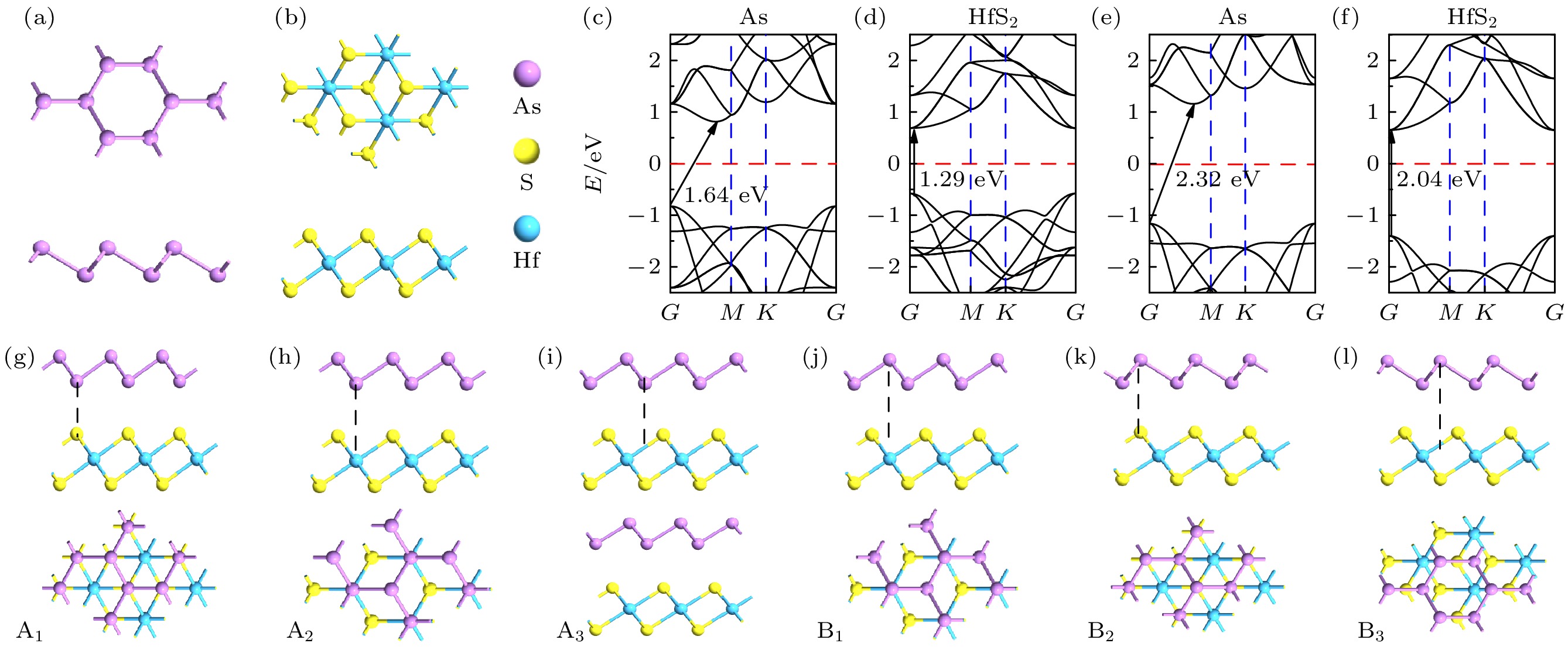
图 1 (a) As单层正视图和侧视图; (b) HfS2单层正视图和侧视图; (c) PBE计算的As单层能带结构; (d) PBE计算的HfS2单层能带结构; (e) HSE06计算的As单层能带结构; (f) HSE06计算的HfS2单层能带结构; (g)–(l) As/HfS2异质结的6种堆叠方式, 分别称为A1—A3和B1—B3
Figure 1. (a) Top and side view of As monolayer; (b) top and side view of HfS2 monolayer; (c) band structure of As monolayer by PBE calculation; (d) band structure of HfS2 monolayer by PBE calculation; (e) band structure of As monolayer by HSE06 calculation; (f) band structure of HfS2 monolayer by HSE06 calculation; (g)–(l) six stacking for As/HfS2 heterostructure, called as A1–A3 and B1–B3, respectively.
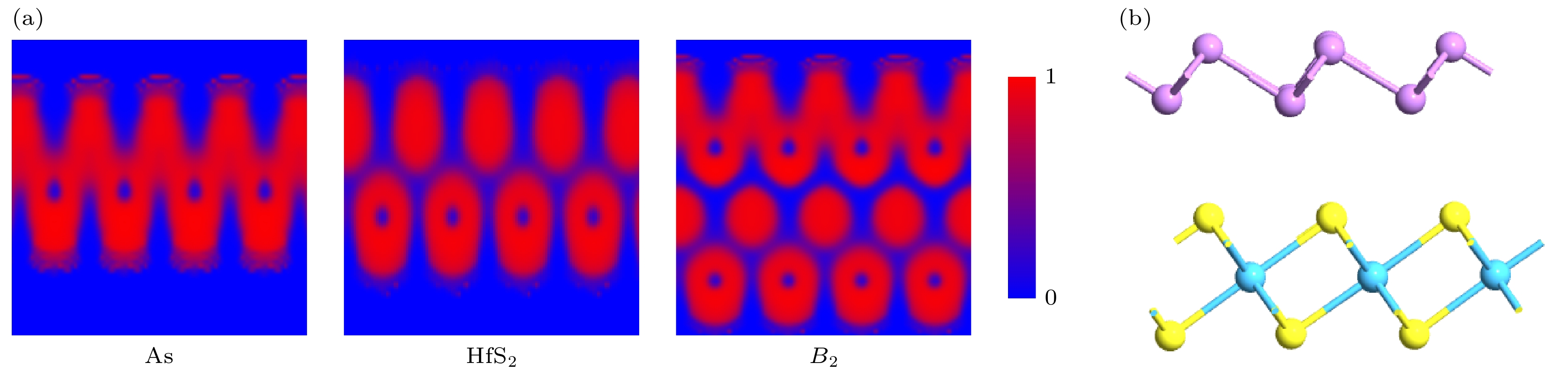
图 2 (a) As与HfS2单层以及As/HfS2异质结的电子局域函数(ELF); (b) B2堆叠的Forcite淬火的分子动力学模拟以检验结构的热稳定性
Figure 2. (a) The electronic localization function (ELF) of As and HfS2 monolayers and As/HfS2 heterostructure; (b) Forcite quenching molecular dynamics simulation for the B2 stacking to examine the structural thermal stability.

图 3 (a) As/HfS2异质结投影能带结构及投影态密度; (b) CBM与VBM的Bloch 态, 等值面为0.035 e/Å3; (c) As/HfS2异质结能带对齐; (d) 沿z轴电荷密度差及三维电荷密度差, 红色和蓝色分别代表电荷积累和消耗, 等值面为3.5×10⁻⁴ e/Å3; (e) 沿z轴方向有效势(eV)分布
Figure 3. (a) Projected band structure and projected state density of As/HfS2 heterostructure; (b) Bloch state for CBM and VBM, the isosurface is set to 0.035 e/A3; (c) band alignment for As/HfS2 heterostructure; (d) charge density difference along the z-axis and three-dimensional charge density difference, red and blue respectively represent charge accumulation and depletion, the isosurface is set to 3.5×10⁻⁴ e/Å3, and (e) electrostatic potential distribution along the z-axis.

图 4 (a)带隙及结合能随应变的变化; (b) 应变 ε = –0.6, –0.4, –0.2, 0, 0.2, 0.4, 0.6 Å 时有效势的变化; (c) 应变ε = –0.8, –0.3, –0.1, 0.1, 0.3, 0.8 Å 时异质结的能带结构, 最高导带上的红点代表VBM的位置
Figure 4. (a) Band gap and binding energy changes with strain; (b) the effective potential distribution along z-axis at ε = –0.6, –0.4, –0.2, 0, 0.2, 0.4 and 0.6 Å, respectively; (c) the As/HfS2 band structure at ε = –0.8, –0.3, –0.1, 0.1, 0.3 and 0.8 Å , respectively, the red dot at top conduction band indicates the VBM position.

图 5 不同垂直应变时的三维电荷密度差 (a) ε = –0.6 Å; (b) ε = –0.2 Å; (c) ε = 0.2 Å; (d) ε = 0.6 Å
Figure 5. Three dimensional charge density difference at (a) ε = –0.6 Å, (b) ε = –0.2 Å, (c) ε = 0.2 Å, (d) ε = 0.6 Å, respectively.

图 6 (a) 异质结外加电场方向示意图; (b)异质结带隙随外电场变化; (c) As与HfS2单层带边(VBM及CBM)位置以及能带对齐方式随外电场的变化; (d) 0.6 V/Å电场时, 异质结的电荷密度差; (e) –0.6 V/Å电场时, 异质结的电荷密度差; (f) 异质结电荷密度差随电场的变化趋势
Figure 6. (a) Schematic diagram of applied external electric field on heterostructure; (b) band gap variation of heterostructure with electric field; (c) evolution of band edges (VBM and CBM) for As and HfS2 monolayers and heterostructure and its band alignment manner with electric field. The charge density difference of heterostructure at: (d) Eext = 0.6 eV/Å, (e) Eext = –0.6 eV/Å, and (f) various electric field.
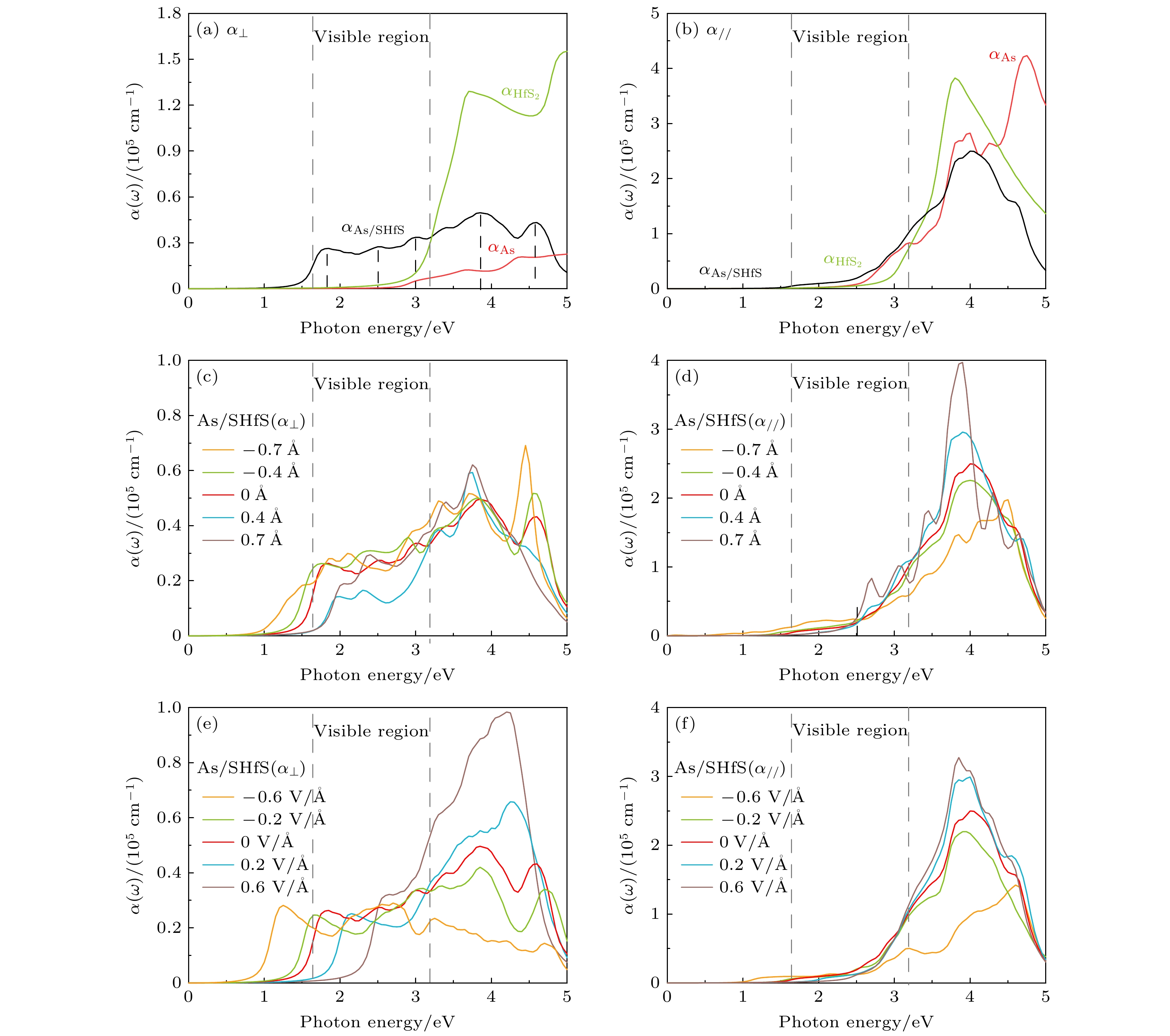
图 7 光吸收系数及调控效应 (a), (b)单层及本征异质结; (c), (d)应变调控的异质结; (e), (f)电场调控的异质结
Figure 7. Light absorption coefficients and tuning effects: (a), (b) The monolayer and intrinsic heterostructure; (b), (c) strain tuning effects; (e), (f) the electric field tuning effects .
表 1 不同堆叠异质结的结合能、层间距和带隙
Table 1. The binding energy, interlayer spacing and band gap for various stacking configurations.
Structure A1 A2 A3 B1 B2 B3 Eb/(meV·Å–2) –14.59 –8.81 –11.26 –8.93 –16.19 –11.71 d/Å 3.1 3.6 3.4 3.6 3.0 3.4 Gap/eV 0.94 1.12 1.04 1.15 0.84 1.06  DownLoad: CSV
-
[1] Gupta A, Sakthivel T, Seal S 2015 Prog. Mater. Sci. 73 44
Google Scholar
[2] Yang L, Chen W, Yu Q, Liu B 2021 Nano Res. 14 1583
Google Scholar
[3] Zhang R W, Zhang C W, Ji W X, Hu S J, Yan S S, Li S S, Li P, Wang P J, Liu Y S 2014 J. Phys. Chem. C 118 25278
Google Scholar
[4] Ni Z Y, Liu Q H, Tang K H, Zheng J X, Zhou J, Qin R, Gao Z X, Yu D P, Lu J 2012 Nano. Lett. 12 113
Google Scholar
[5] Massicotte M, Soavi G, Principi A, Tielrooij K J 2021 Nanoscale 13 8376
Google Scholar
[6] Blase X, Rubio A, Louie S G, Cohen M L, 1995 Phys. Rev. B 51 6868
Google Scholar
[7] Cahangirov S, Topsakal M, Aktürk E, Sahin H, Ciraci S 2009 Phys. Rev. Lett 102 236804
Google Scholar
[8] Kuang W, Hu R, Fan Z, Zhang Z 2019 Nanotechnology 30 145201
Google Scholar
[9] Xiao D, Liu G B, Feng W, Xu X, Yao W 2012 Phys. Rev. Lett 108 196802
Google Scholar
[10] Li X, Zhu H 2015 J. Materiomics 1 33
Google Scholar
[11] Yang G, Li L H, Lee W B, Ng M C 2018 Sci. Technol. Adv. Mater. 19 613
Google Scholar
[12] Low J, Yu J, Jaroniec M, Wageh S, Al‐Ghamdi A A 2017 Adv. Mater. 29 1601694
Google Scholar
[13] Wang H, Zhang L, Chen Z, Hu J Q, Li S J, Wang Z H, Liu J S, Wang X C 2014 Chem. Soc. Rev. 43 5234
Google Scholar
[14] Yan J A, Stein R, Schaefer D M, Wang X Q, Chou M Y 2013 Phys. Rev. B 88 121403
Google Scholar
[15] She L, Zhang F, Jia C, Kang L, Li Q, He X, Sun J, Lei Z, Liu Z 2021 Nanoscale 13 15781
Google Scholar
[16] He C, Zhang J H, Zhang W X, Li T T 2019 J. Phys. Chem. Lett. 10 3122
Google Scholar
[17] He C, Han F, Zhang W 2021 Chin. Chem. Lett. 33 404
[18] Li X, Li Z, Yang J 2014 Phys. Rev. Lett. 112 018301
Google Scholar
[19] Song W, Chen J, Li Z, Fang X 2021 Adv. Mater. 33 2101059
Google Scholar
[20] Chen F, Shi D, Yang M, Jiang H, Shao Y, Wang S, Zhang B, Shen J, Wu Y, Hao X 2021 Adv. Fun. Mater. 31 2007132
Google Scholar
[21] Peng D, Wang Y, Shi H, Wei J, Tao J, Zhao H, Chen Z 2022 J. Colloid Interface Sci. 613 194
Google Scholar
[22] Meitl M A, Zhu Z T, Kumar V, Lee K J, X. Feng, Huang Y Y, Adesida I, Nuzzo R G, Rogers J A 2006 Nat. Mater. 5 33
Google Scholar
[23] Castellanos-Gomez A, Buscema M, Molenaar R, Singh V, Janssen L, van der Zant H S J, Steele G A 2014 2D Mater. 1 011002
Google Scholar
[24] Gong Y, Lin J, Wang X, et al. 2014 Nat. Mater. 13 1135
Google Scholar
[25] Wang Y, Zhang C, Ji W, Wang P 2015 Appl. Phys. Express 8 065202
Google Scholar
[26] Kecik D, Durgun E, Ciraci S 2016 Phys. Rev. B 94 205410
Google Scholar
[27] Li Z J, Xu W, Yu Y Q, Du H Y, Zhen K, Wang J, Luo L B, Qiu H L, Yang X B, 2016 J. Mater. Chem. A 4 362
Google Scholar
[28] Xu C, Zhu M, Zheng H, Du X, Wang W, Yan Y 2016 RSC Adv. 6 43794
Google Scholar
[29] Sahin H, Sivek J, Li S, Partoens B, Peeters F M 2013 Phys. Rev. B 88 045434
Google Scholar
[30] Li Y, Xia C X, Wang T X, Tan X M, Zhao X, Wei S Y 2016 Solid State Commun. 230 6
Google Scholar
[31] Han J N, Zhang Z H, Fan Z Q, Zhou R L 2020 Nanotechnology 31 315206
Google Scholar
[32] Xie Z F, Sun F W, Yao R, Zhang Y, Zhang Y H, Zhang Z H, Fang Z B, Ni L, Duan L 2019 Appl. Surf. Sci. 475 839
Google Scholar
[33] Nie X R, Sun B Q, Zhu H, Zhang M, Zhao D H, Chen L, Sun Q Q, Zhang D W 2017 ACS Appl. Mater. Interfaces 9 26996
Google Scholar
[34] Kanazawa T, Amemiya T, Ishikawa A, Upadhyaya V, Tsuruta K, Tanaka T, Miyamoto Y 2016 Sci. Rep. 6 1
Google Scholar
[35] Fu L, Wang F, Wu B, Huang W 2017 Adv. Mater. 29 1700439
Google Scholar
[36] Xu K, Wang Z, Wang F, Huang Y, Wang F, Yin L, Jiang C, He J 2015 Adv. Mater. 27 7881
Google Scholar
[37] Wang B, Wang X, Wang P, Yang T, Yuan H, Wang H, Wang G, Chen H 2019 Nanomaterials 9 1706
Google Scholar
[38] Fu C F, Wu X, Yang J. 2018 Adv. Mater. 30 1802106
Google Scholar
[39] King'ori G W, Ouma C N M, Mishra A K, Amolo G O, Makau N W T 2020 RSC Adv. 10 30127
Google Scholar
[40] Lei C, Ma Y, Xu X, Zhang T, Huang B, Dai Y 2019 J. Phys. Chem. C 123 23089
Google Scholar
[41] Brandbyge M, Mozos J L, Ordejón P, Taylor J, Stokbro K 2002 Phys. Rev. B 65 165401
Google Scholar
[42] Hu R, Wang D, Fan Z Q, Zhang Z H 2018 Phys. Chem. Chem. Phys. 20 13574
Google Scholar
[43] 李野华, 范志强, 张振华 2019 物理学报 68 198503
Google Scholar
Li Y H, Fan Z Q, Zhang Z H 2019 Acta Phys. Sin. 68 198503
Google Scholar
[44] Zhao T, Fan Z Q, Zhang Z H, Zhou R L 2019 J. Phys. D Appl. Phys. 52 475301
Google Scholar
[45] Hu R, Li Y H, Zhang Z H, Fan Z Q, Sun L 2019 J. Mater. Chem. C 7 7745
Google Scholar
[46] He X, Deng X Q, Sun L, Zhang Z H, Fan Z Q 2022 Appl. Surf. Sci. 578 151844
Google Scholar
[47] Han J N, He X, Fan Z Q, Zhang Z H 2019 Phys. Chem. Chem. Phys. 21 1830
Google Scholar
[48] 徐永虎, 邓小清, 孙琳, 范志强, 张振华 2022 物理学报 71 046102
Google Scholar
Xu Y H, Deng X Q, Sun L, Fang Z Q, Zhang Z H 2022 Acta Phys. Sin. 71 046102
Google Scholar
[49] Grimme S 2006 J. Comput. Chem. 27 1787
Google Scholar
[50] Zhao J, Qi Z H, Xu Y, Dai J, Zeng X C, Guo W, Ma J 2019 Wiley Interdiscip. Rev. Comput. Mol. Sci. 9 e1387
[51] Kamal C, Ezawa M 2015 Phys. Rev. B 91 085423
Google Scholar
[52] Deng S, Li L, Rees P 2019 ACS Appl. Nano Mater. 2 3977
Google Scholar
[53] Zheng X, Wei Y, Pang K, Tolbert N K, Kong D, Xu X, Yang J, Li X, Li W 2020 Sci. Rep. 10 1
Google Scholar
[54] Huang L, Huo N, Li Y, Chen H, Yang J, Wei Z, Li J, Li S 2015 J. Phys. Chem. Lett. 6 2483
Google Scholar

 DownLoad:
Catalog
Metrics
- Abstract views: 2955
- PDF Downloads: 84
- Cited By: 0
