


-
With the development of nanoscale circuit technology, the on-track error rate of digital circuit and the effect of single event upset have become more pronounced. The radiation resistance research on DICE SRAM or DICE flip-flop device has been carried out extensively, including 65 nm, 90 nm, and 130 nm. However, the research on 55 nm DICE latch has not been reported. Using a three-dimensional device model of the 55 nm bulk silicon process established by the simulation tool TCAD, we verify the reinforcement performance of the DICE circuit, and clarify the effects of different incident conditions on DICE circuits. At the same time, we carry out a comparison of anti-SEU performance between NMOS transistor and PMOS transistor in the 55 nm process through comparative simulation experiments and quantitative analysis. The result shows that one of the important factors is the LET value which affects the generation rate of electron-hole pairs. A higher LET value will extend the upset recovery time of device and increase the peak of voltage. In addition, the difference in charge-sharing mechanism between transistors leads to the recovery time of PMOS higher than that of NMOS. As the angle of incidence increases, the charge-sharing mechanism between adjacent devices is enhanced, and electron-hole pairs ionized in sensitive regions increase. Due to the difference in charge mobility, the sensitivity of the angle of incidence of Nhit in DICE is much greater than that of Phit. Therefore, strict tilt angle incident test evaluation is required for DICE device before practical application. Finally, the large distance between adjacent MOS tubes will weaken the charge-sharing mechanism and reduce the charge collection of adjacent MOS tubes. Simulation result shows that the distance between the MOS transistors in the 55 nm process cannot be less than 1.2 μm. The relevant simulation results can provide a theoretical basis and data for supporting the study of the physical mechanism of SEU and reinforcement technology, thereby promoting the application of memory devices to the aerospace field.
-
Keywords:
- double interlocked inverter structure /
- numerical simulation /
- single event upset effect /
- charge sharing effect
Erratum: Three-dimensional numerical simulation of single event upset effect based on 55 nm DICE latch unit [Acta Phys. Sin. 2024, 73(6): 066103]
Zhang Xing, Liu Yu-Lin, Li Gang, Yan Shao-An, Xiao Yong-Guang, Tang Ming-Hua. Erratum: Three-dimensional numerical simulation of single event upset effect based on 55 nm DICE latch unit [Acta Phys. Sin. 2024, 73(7): 079901]. Acta Phys. Sin., 2024, 73(7): 079901. doi: 10.7498/aps.73.079901
[1] Lu Y F, Zhai X J, Saha S, Ehsan S, McDonald-Maier K 2022 IEEE Syst. J. 16 1436
 Google Scholar
[2] Rathore P, Nakhate S 2016 IEEE 1st International Conference on Power Electronics, Intelligent Control and Energy Systems Delhi, India, July 4–6, 2016 p38
[3] Trivedi R, Devashrayee N M, Mehta U S, Desai N M, Patel H 2015 19th International Symposium on VLSI Design and Test Ahmedabad, India, June 26–29, 2015 p46
[4] Li H S, Wu L S, Yang B, Jiang Y H 2017 J. Semicond. 38 085009
Google Scholar
[5] 李海松, 杨博, 蒋轶虎, 高利军, 杨靓 2022 电子科技大学学报 51 458
Li H S, Yang B, Jiang Y H, Gao L J, Yang L 2022 J. UEST China 51 458
[6] 江新帅, 罗尹虹, 赵雯, 张凤祁, 王坦 2023 物理学报 72 036101
Google Scholar
Jiang X S, Luo Y H, Zhao W, Zhang F Q, Wang T 2023 Acta Phys. Sin. 72 036101
Google Scholar
[7] Chi Y Q, Cai C, He Z, Wu Z Y, Fang Y H, Chen J J, Liang B 2022 Electronics 11 972
Google Scholar
[8] Lin T, Chong K, Shu W, Lwin N K Z, Jiang J Z, Chang J S 2016 IEEE International Symposium on Circuits and Systems Montreal, QC, Canada, May 22–25, 2016 p966
[9] Diggins Z J, Gaspard N J, Mahatme N N, Jagannathan S, Loveless T D, Reece T R, Bhuva B L, Witulski A F, Massengill L W, Wen S J, Wong R 2013 IEEE Trans. Nucl. Sci. 60 4394
Google Scholar
[10] Moradi F, Panagopoulos G, Karakonstantis G, Farkhani H, Wisland D T, Madsen J K, Mahmoodi H, Roy K 2014 Microelectron. J. 45 23
Google Scholar
[11] Maru A, Shindou H, Ebihara T, Makihara A, Hirao T, Kuboyama S 2010 IEEE Trans. Nucl. Sci. 57 3602
Google Scholar
[12] Xu H, Zeng Y, Liang B 2015 IEICE Electron. Expr. 12 20150629
Google Scholar
[13] Luo Y Y, Zhang F Q, Wei C, Ding L L, Pan X Y 2019 Microelectron. Reliab. 94 24
Google Scholar
[14] Hsiao S M H, Wang L P T, Liang A C W, Wen C H P 2022 IEEE International Test Conference Anaheim, CA, USA, August 24–26, 2022 p128
[15] 罗尹虹, 张凤祁, 郭红霞, Wojtek Hajdas 2020 物理学报 69 018501
Google Scholar
Luo Y H, Zhang F Q, Guo H X, Wojtek H 2020 Acta Phys. Sin. 69 018501
Google Scholar
[16] He Z, Zhao S W, Cai C, Yan X Y, Liu Y Z, Gao J L S 2021 Nucl. Sci. Tech. 32 139
Google Scholar
[17] 琚安安, 郭红霞, 张凤祁, 刘晔, 钟向丽, 欧阳晓平, 丁李利, 卢超, 张鸿, 冯亚辉 2023 物理学报 72 026102
Google Scholar
Ju A A, Guo H X, Zhang F Q, Liu Y, Zhong X L, Ouyang X P, Ding L L, Lu C, Zhang H, Feng Y H 2023 Acta Phys. Sin. 72 026102
Google Scholar
[18] Dodd P E 2006 IEEE T. Device. Mat. Re.5 343
Google Scholar
[19] Maru A, Matsuda A, Kuboyama S, Yoshimoto M 2022 IEICE T. Electron. E105-C 47
Google Scholar
[20] Wang J, Li L 2014 15th International Conference on Electronic Packaging Technology Chengdu, China, August 12–15, 2014 p1116
-

图 1 MOS管电流-电压特性校准结果 (a) nfet器件Id -Vd校准曲线; (b) nfet器件Id -Vg校准曲线; (c) pfet器件Id -Vd校准曲线; (d) pfet器件Id -Vg校准曲线
Figure 1. Current-voltage characteristics calibration results of MOS tube: (a) The Id -Vd calibration curve of nfet device; (b) the Id -Vg calibration curve of nfet device; (c) the Id -Vd calibration curve of pfet device; (d) the Id-Vg calibration curve of pfet device.

图 2 标准锁存单元电路原理图(VDD, 电源电压; VSS, 接地端电压; CLK1/CLK2, 时钟信号) (a) 标准锁存单元电路中粒子轰击MN1漏极; (b) 标准锁存单元电路中粒子轰击MP2漏极
Figure 2. Circuit diagram of standard latch cell: (a) Particle bombards the drain of MN1 in the standard latch cell circuit; (b) particle bombards the drain of MP2 in the standard latch cell circuit. VDD, power voltage; VSS, ground terminal voltage; CLK1/CLK2, clock signal.
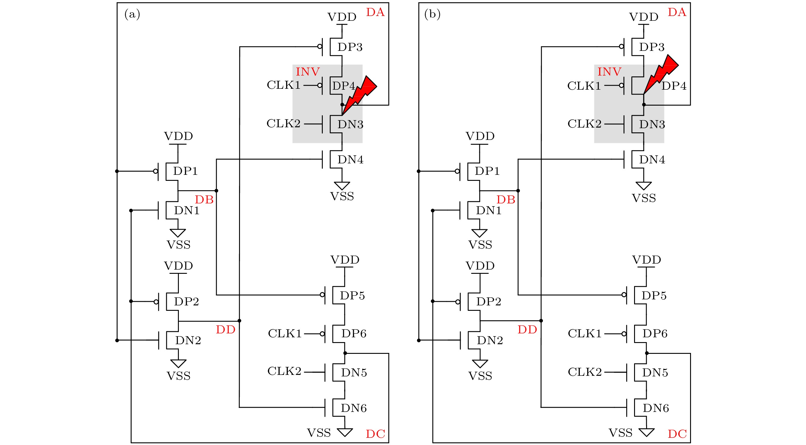
图 3 DICE结构电路原理图 (a)粒子轰击DICE电路中DN3漏极; (b)粒子轰击DICE电路中DP4漏极
Figure 3. Circuit diagrams of DICE structure: (a) Particle bombards the drain of DN3 in DICE circuit; (b) particle bombards the drain of DP4 in DICE circuit.

图 4 粒子轰击标准锁存单元中MN1漏极D1, D2节点电压变化
Figure 4. Transient voltage change of D1 and D2 nodes when particle bombards the drain of MN1 in the standard latch cell circuit.
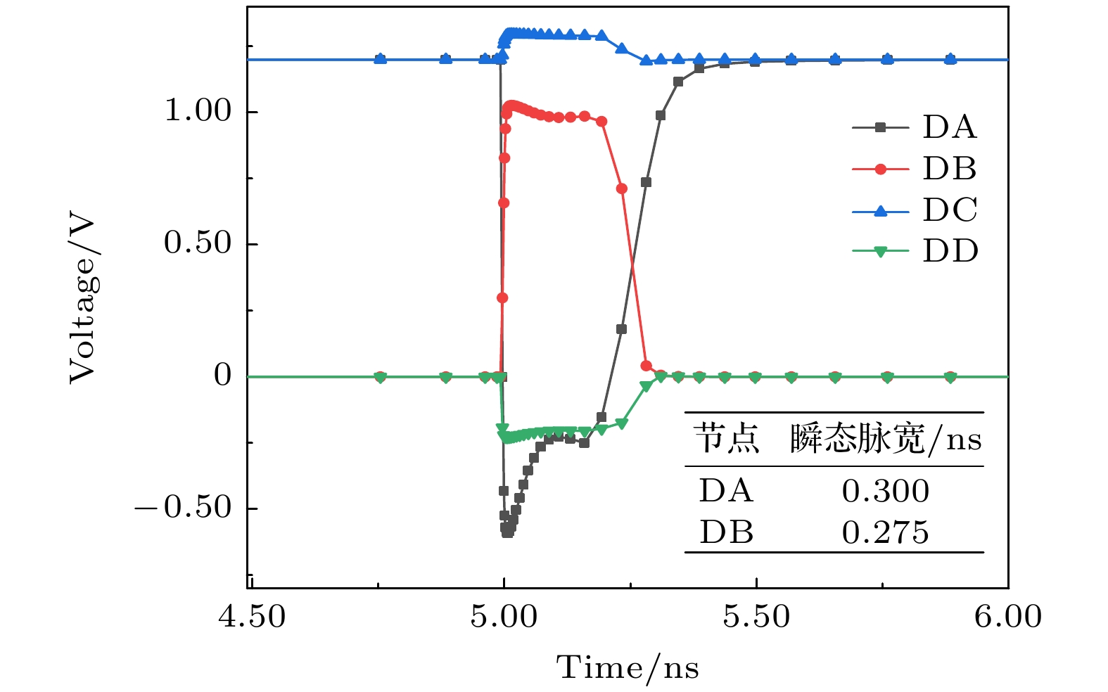
图 5 DICE电路中粒子轰击DN3漏极各节点电压变化
Figure 5. Voltage variation of each node when particle bombards the drain of DN3 in the DICE circuit.

图 6 DICE电路原理图 (a)粒子轰击DICE电路中DN3漏极; (b)粒子轰击DICE电路中DP4漏极
Figure 6. Circuit diagrams of DICE: (a) Particle bombards the drain of DN3 in DICE circuit; (b) particle bombards the drain of DP4 in DICE circuit.

图 7 不同LET值入射时DA节点电位变化图 (a) 轰击DN3晶体管时DA节点的电位变化图; (b) 轰击DP4晶体管时DA节点的电位变化图
Figure 7. Voltage variation diagram of DA node when particle incidents by different LET value: (a) Voltage variation diagram of DA node when bombarding DN3 transistor; (b) voltage variation diagram of DA node when bombarding DP4 transistor.

图 8 粒子不同方位角入射示意图
Figure 8. Diagram of particle incidents from different angles.

图 9 不同角度入射时主、从器件电位变化图 (a) 轰击DN3管漏极时主器件电位变化图; (b) 轰击DN3管漏极时从器件电位变化图; (c) 轰击DP4管漏极时主器件电位变化图; (d) 轰击DP4管漏极时从器件电位变化图
Figure 9. Voltage variation diagrams of master and slave devices when particle incidents from different angles: (a) Voltage variation diagram of the master device when particle bombards the drain of DN3; (b) voltage variation diagram of the slave device when particle bombards the drain of the DN3; (c) voltage variation diagram of the master device when particle bombards the drain of the DP4; (d) voltage variation diagram of the slave device when particle bombards the drain of DP4.

图 10 器件模型示意图 (a) 二维横截面图; (b) 二维俯视图
Figure 10. Device model schematic: (a) 2D cross-sectional view; (b) 2D top view.
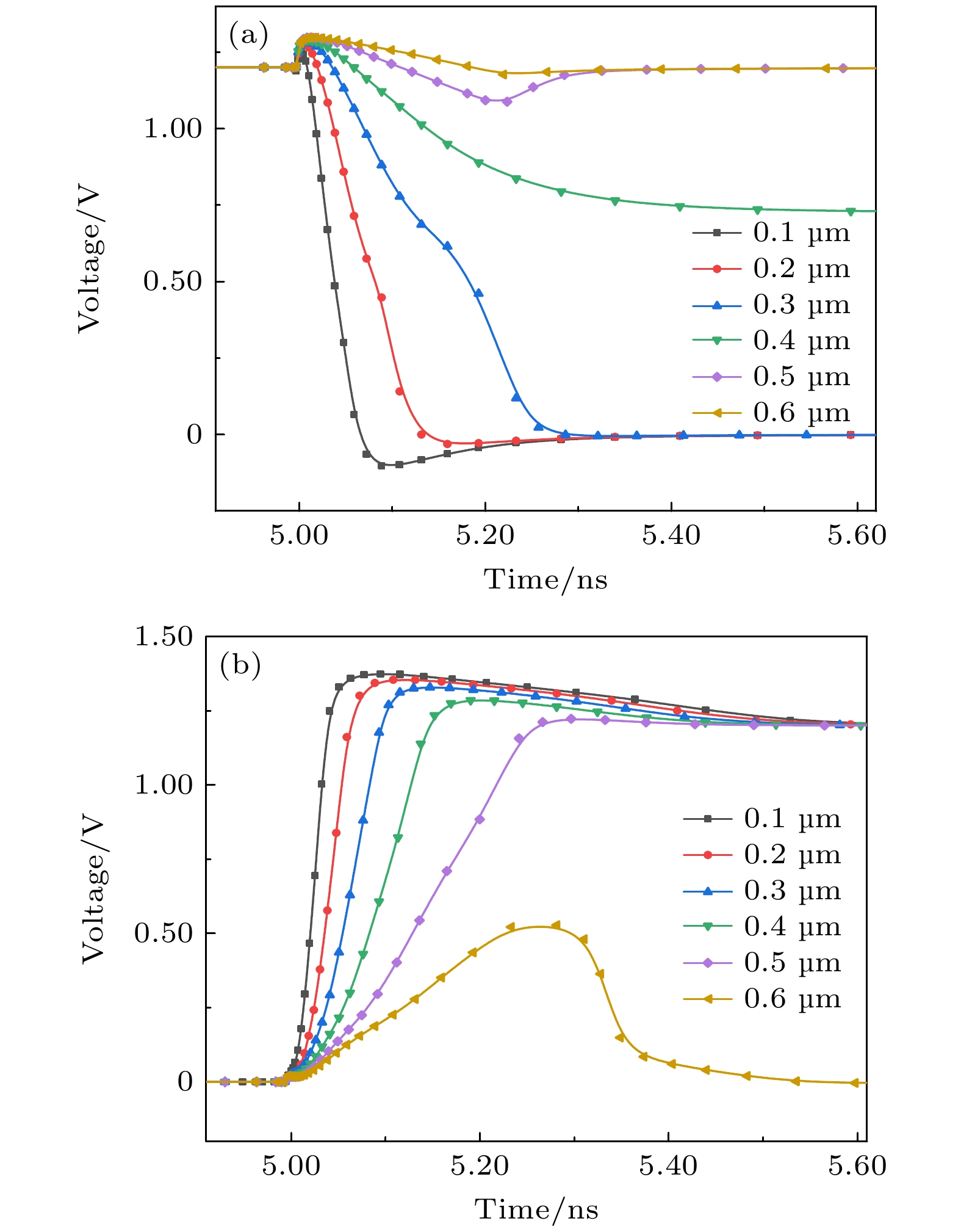
图 11 MOS管漏极间距对电压脉冲的影响 (a) 轰击DN3管漏极时从器件电位变化图; (b) 轰击DP4管漏极时从器件电位变化图
Figure 11. Influence of the distance between the drain of MOS tubes on the transient pulse: (a) Slave device voltage change diagram when bombarding the drain of the DN3 tube; (b) slave device voltage change diagram when bombarding the drain of the DP4 tube.
表 1 55 nm MOS晶体管工艺参数
Table 1. 55 nm MOS transistor process parameters.
名称 NMOS (nfet) PMOS (pfet) 栅长/nm 60 60 栅极氧化物厚度/m 2.6×10⁻⁹ 2.8×10⁻⁹ 源极/漏极结深/m 1.0×10⁻⁷ 1.0×10⁻⁸ 多晶硅栅极掺杂浓度/cm–3 1.0×10²¹ 2.6×10²⁰ 沟道掺杂浓度/cm–3 3.2×10¹⁷ 2.0×10¹⁸ 源极/漏极掺杂浓度/cm–3 1.0×10²⁰ 1.0×10²⁰  DownLoad: CSV
表 2 DICE电路中NMOS的翻转阈值
Table 2. Toggle threshold of NMOS in DICE circuit.
入射角度/(°) NMOS管间距/μm 0.4 0.8 1.2 LET阈值/
(MeV·cm2·mg–1)0 14 50+ 50++ 30 10 22 50+ 45 5 13 30 60 4 6 10
DownLoad: CSV
表 3 DICE电路中PMOS的翻转阈值
Table 3. Toggle threshold of PMOS in DICE circuit.
入射角度/(°) PMOS管间距/μm 0.4 0.8 1.2 LET阈值/
(MeV·cm2·mg–1)0 10 23 50+ 30 9 16 32 45 8 12 19 60 7 9 16
DownLoad: CSV
-
[1] Lu Y F, Zhai X J, Saha S, Ehsan S, McDonald-Maier K 2022 IEEE Syst. J. 16 1436
Google Scholar
[2] Rathore P, Nakhate S 2016 IEEE 1st International Conference on Power Electronics, Intelligent Control and Energy Systems Delhi, India, July 4–6, 2016 p38
[3] Trivedi R, Devashrayee N M, Mehta U S, Desai N M, Patel H 2015 19th International Symposium on VLSI Design and Test Ahmedabad, India, June 26–29, 2015 p46
[4] Li H S, Wu L S, Yang B, Jiang Y H 2017 J. Semicond. 38 085009
Google Scholar
[5] 李海松, 杨博, 蒋轶虎, 高利军, 杨靓 2022 电子科技大学学报 51 458
Li H S, Yang B, Jiang Y H, Gao L J, Yang L 2022 J. UEST China 51 458
[6] 江新帅, 罗尹虹, 赵雯, 张凤祁, 王坦 2023 物理学报 72 036101
Google Scholar
Jiang X S, Luo Y H, Zhao W, Zhang F Q, Wang T 2023 Acta Phys. Sin. 72 036101
Google Scholar
[7] Chi Y Q, Cai C, He Z, Wu Z Y, Fang Y H, Chen J J, Liang B 2022 Electronics 11 972
Google Scholar
[8] Lin T, Chong K, Shu W, Lwin N K Z, Jiang J Z, Chang J S 2016 IEEE International Symposium on Circuits and Systems Montreal, QC, Canada, May 22–25, 2016 p966
[9] Diggins Z J, Gaspard N J, Mahatme N N, Jagannathan S, Loveless T D, Reece T R, Bhuva B L, Witulski A F, Massengill L W, Wen S J, Wong R 2013 IEEE Trans. Nucl. Sci. 60 4394
Google Scholar
[10] Moradi F, Panagopoulos G, Karakonstantis G, Farkhani H, Wisland D T, Madsen J K, Mahmoodi H, Roy K 2014 Microelectron. J. 45 23
Google Scholar
[11] Maru A, Shindou H, Ebihara T, Makihara A, Hirao T, Kuboyama S 2010 IEEE Trans. Nucl. Sci. 57 3602
Google Scholar
[12] Xu H, Zeng Y, Liang B 2015 IEICE Electron. Expr. 12 20150629
Google Scholar
[13] Luo Y Y, Zhang F Q, Wei C, Ding L L, Pan X Y 2019 Microelectron. Reliab. 94 24
Google Scholar
[14] Hsiao S M H, Wang L P T, Liang A C W, Wen C H P 2022 IEEE International Test Conference Anaheim, CA, USA, August 24–26, 2022 p128
[15] 罗尹虹, 张凤祁, 郭红霞, Wojtek Hajdas 2020 物理学报 69 018501
Google Scholar
Luo Y H, Zhang F Q, Guo H X, Wojtek H 2020 Acta Phys. Sin. 69 018501
Google Scholar
[16] He Z, Zhao S W, Cai C, Yan X Y, Liu Y Z, Gao J L S 2021 Nucl. Sci. Tech. 32 139
Google Scholar
[17] 琚安安, 郭红霞, 张凤祁, 刘晔, 钟向丽, 欧阳晓平, 丁李利, 卢超, 张鸿, 冯亚辉 2023 物理学报 72 026102
Google Scholar
Ju A A, Guo H X, Zhang F Q, Liu Y, Zhong X L, Ouyang X P, Ding L L, Lu C, Zhang H, Feng Y H 2023 Acta Phys. Sin. 72 026102
Google Scholar
[18] Dodd P E 2006 IEEE T. Device. Mat. Re.5 343
Google Scholar
[19] Maru A, Matsuda A, Kuboyama S, Yoshimoto M 2022 IEICE T. Electron. E105-C 47
Google Scholar
[20] Wang J, Li L 2014 15th International Conference on Electronic Packaging Technology Chengdu, China, August 12–15, 2014 p1116

 DownLoad:
Catalog
Metrics
- Abstract views: 590
- PDF Downloads: 25
- Cited By: 0
