


-
Orientationally ordered liquid crystals (LCs) exhibit remarkable physical anisotropy and responsiveness to external fields, which give rise to distinguished physical effects and have led to the emergence of a new generation of electric-optical applications. The LCs are also renowned for their abundance of phases and topological defects, which are of significance in studying both fundamental science and practical technology. One simple approach to generating umbilic defects involves applying an electric field to a homeotropically aligned nematic LC with negative dielectric anisotropy
$\Delta \varepsilon $ . However, the influence of material properties and external conditions on the dynamic process of nematic LC defects remains unclear. Here, we select seven kinds of nematic LCs with negative dielectrically anisotropy, ranging from –1.1 to –11.5, to explore the dynamics of electric-field-induced umbilics. By using a linearly increasing electric field parallel to the molecular orientation of LC, we systematically investigate the effects of material property (dielectric anisotropy) and external conditions (temperature and electric field parameters) on the formation and annihilation of umbilic defects. The experimental results show that the dynamic process of forming the umbilic defects in nematic LCs is independent of dielectric anisotropy, temperature, and electric field frequency, but follows the Kibble-Zurek mechanism, in which the density of generated umbilic defects exhibits a power-law scaling with the change of the electric field ramp rate, with a scaling exponent of approximately$1/2$ . Interestingly, a stronger dielectric anisotropy leads to a higher density of umbilic defects. Additionally, a change in temperature has a significant influence on the density of umbilic defects , in which higher temperature leads to greater defect density under the same external electric field conditions. Furthermore, the annihilation rate of umbilic defects is closely related to the material properties and the ramp of the applied electric field. Specifically, the annihilation rate of umbilic defects becomes faster when dielectric anisotropy is stronger or the electric field ramp is larger. This study provides valuable insights into the relationship between the formation and annihilation of defects, material properties, and external conditions in nematic LCs with dielectrically negative anisotropy, contributing to our comprehensive understanding of the dynamic process of topological defects in soft matter.[1] Li J, Bisoyi H K, Tian J, Guo J, Li Q 2019 Adv. Mater. 31 1807751
 Google Scholar
[2] Wang J W, Li K, He H I, Cai W F, Liu J X, Yin Z, Mu Q Q, Hisao V K S, Gérard D, Luo D, Li G, Liu Y J 2022 Laser Photonics Rev. 16 2100396
Google Scholar
[3] Yang C, Wu B, Ruan J, Zhao P, Chen L, Chen D, Ye F 2021 Adv. Mater. 33 2006361
Google Scholar
[4] Li X, Ma S, Hu J, Ni Y, Lin Z, Yu H 2019 J. Mater. Chem. C 7 622
Google Scholar
[5] Hu J, Yu M, Wang M, Choy K L, Yu H 2022 ACS Appl. Mater. Interfaces 14 12951
Google Scholar
[6] Ji Z C, Zhang X Z, Zhang Y J, Wang Z H, Drevensek-Olenik I, Rupp R, Li W, Wu Q, Xu J J 2017 Chin. Opt. Lett. 15 070501
Google Scholar
[7] 王磊, 肖芮文, 葛士军, 沈志雄, 吕鹏, 胡伟, 陆延青 2019 物理学报 68 084205
Google Scholar
Wang L, Xiao R W, Ge S J, Shen Z X, Lü P, Hu W, Lu Y Q 2019 Acta Phys. Sin. 68 084205
Google Scholar
[8] 朱雨雯, 袁丛龙, 刘炳辉, 王骁乾, 郑致刚 2019 物理学报 72 174206
Google Scholar
Zhu Y W, Yuan C L, Liu B H, Wang X Q, Zheng Z G 2019 Acta Phys. Sin. 72 174206
Google Scholar
[9] Zurek WH 1985 Nature 317 505
Google Scholar
[10] Kibble TWB 1976 J. Phys. A: Math. Gen. 9 1387
Google Scholar
[11] del Campo A, Zurek WH 2014 Int. J. Mod. Phys. A 29 1430018
Google Scholar
[12] 张馨元, 崔慧林, 王钰, 陈宏一, 张心正 2022 液晶与显示 37 1032
Google Scholar
Zhang X Y, Cui H L, Wang Y, Chen H Y, Zhang X Z 2022 Chin. J. Liq. Cryst. Disp. 37 1032
Google Scholar
[13] Ohzono T, Katoh K, Wang C, Fukazawa A, Yamaguchi S, Fukuda J 2017 Sci. Rep. 7 16814
Google Scholar
[14] Rapini A 1973 J. Phys. France. 34 629
Google Scholar
[15] Wu S B, Wu J B, Cao H M, Lu Y Q, Hu W 2023 Phys. Rev. Lett. 130 078101
Google Scholar
[16] Fumeron S, Berche B 2023 Eur. Phys. J. Spec. Top. 232 1813
Google Scholar
[17] de Oliveira B F, Avelino P P, Moraes F, Oliveira J C R E 2010 Phys. Rev. E 82 041707
Google Scholar
[18] Shen Y, Dierking I 2019 Soft Matter 15 8749
Google Scholar
[19] Pismen LM, Rubinstein BY 1992 Phys. Rev. Lett. 69 96
Google Scholar
[20] Williams C, Pierański P, Cladis P E 1972 Phys. Rev. Lett. 29 90
Google Scholar
[21] Chuang I, Turok N, Yurke B 1991 Phys. Rev. Lett. 66 2472
Google Scholar
[22] Osterman N, Kotar J, Terentjev E M, Cicuta P 2010 Phys. Rev. E 81 061701
Google Scholar
[23] Harth K, Stannarius R 2020 Front. Phys. 8 112
Google Scholar
[24] Zhang Y H, Deserno M, Tu Z C 2020 Phys. Rev. E 102 012607
Google Scholar
[25] Grollau S, Abbott N L, de Pablo J J 2003 Phys. Rev. E 67 051703
Google Scholar
[26] Svenšek D, Žumer S 2002 Phys. Rev. E 66 021712
Google Scholar
[27] Bogi A, Martinot-Lagarde P, Dozov I, Nobili M 2002 Phys. Rev. Lett. 89 225501
Google Scholar
[28] Oswald P, Ignés-Mullol J 2005 Phys. Rev. Lett. 95 027801
Google Scholar
[29] Zurek WH 1996 Phys. Rep. 276 177
Google Scholar
[30] Dziarmaga J 2010 Adv. Phys. 59 1063
Google Scholar
[31] Kleman M, Lavrentovich OD 2006 Philos. Mag. 86 4117
Google Scholar
[32] Chuang I, Durrer R, Turok N, Yurke B 1991 Science 251 1336
Google Scholar
[33] Dierking I, Marshall O, Wright J, Bulleid N 2005 Phys. Rev. E 71 061709
Google Scholar
[34] Dierking I, Ravnik M, Lark E, Healey J, Alexander GP, Yeomans J M 2012 Phys. Rev. E 85 021703
Google Scholar
[35] Fowler N, Dierking I 2017 ChemPhysChem 18 812
Google Scholar
[36] Nagaya T, Hotta H, Oriharaand Yoshihiro Ishibashi H 1992 J. Phys. Soc. Jpn. 61 3511
Google Scholar
[37] Toyoki H 1990 J. Phys. Rev. A 42 911
Google Scholar
-

图 1 液晶盒加电前(a)后(b)示意图, 蓝色椭球代表液晶分子, 蓝色双向箭头表示取向方向. 脐点缺陷指向矢分布图 (c) $ S = + 1, $$ {\text{ }}\psi = 0 $; (d) $ S = - 1, {\text{ }}\psi = 0 $, 黑色双向箭头表示交流电场方向. 脐点缺陷$ S = - 1, {\text{ }}\psi = 0 $和$ S = + 1, {\text{ }}\psi = {\text{π }}/6 $的POM图像 (e) 正交偏振片; (f) 全波片(波长为$ {\text{530 nm}} $), 白色虚线代表指向矢场方向. 比例尺: $ {\text{30 μm}} $
Figure 1. The schematic configuration of the liquid crystal cell (a) before application of electric field and (b) under the application of electric field. Blue ellipsoids represent liquid crystal directors. Blue bidirectional arrow denotes the alignment direction. The schematic director field around (c) $ S = + 1, {\text{ }}\psi = 0 $ and (d) $ S = - 1, {\text{ }}\psi = 0 $ topological defects. The black bidirectional arrow denotes the directions of the alternating current field. POM image of $ S = - 1, {\text{ }}\psi = 0 $and $ S = + 1, {\text{ }}\psi = {\text{π }}/6 $umbilic defects (e) with crossed polarizers and (f) a full-wave plate of wavelength $ {\text{530 nm}} $. The white dotted line denotes the direction of director. Scale bar: $ {\text{30 μm}} $.
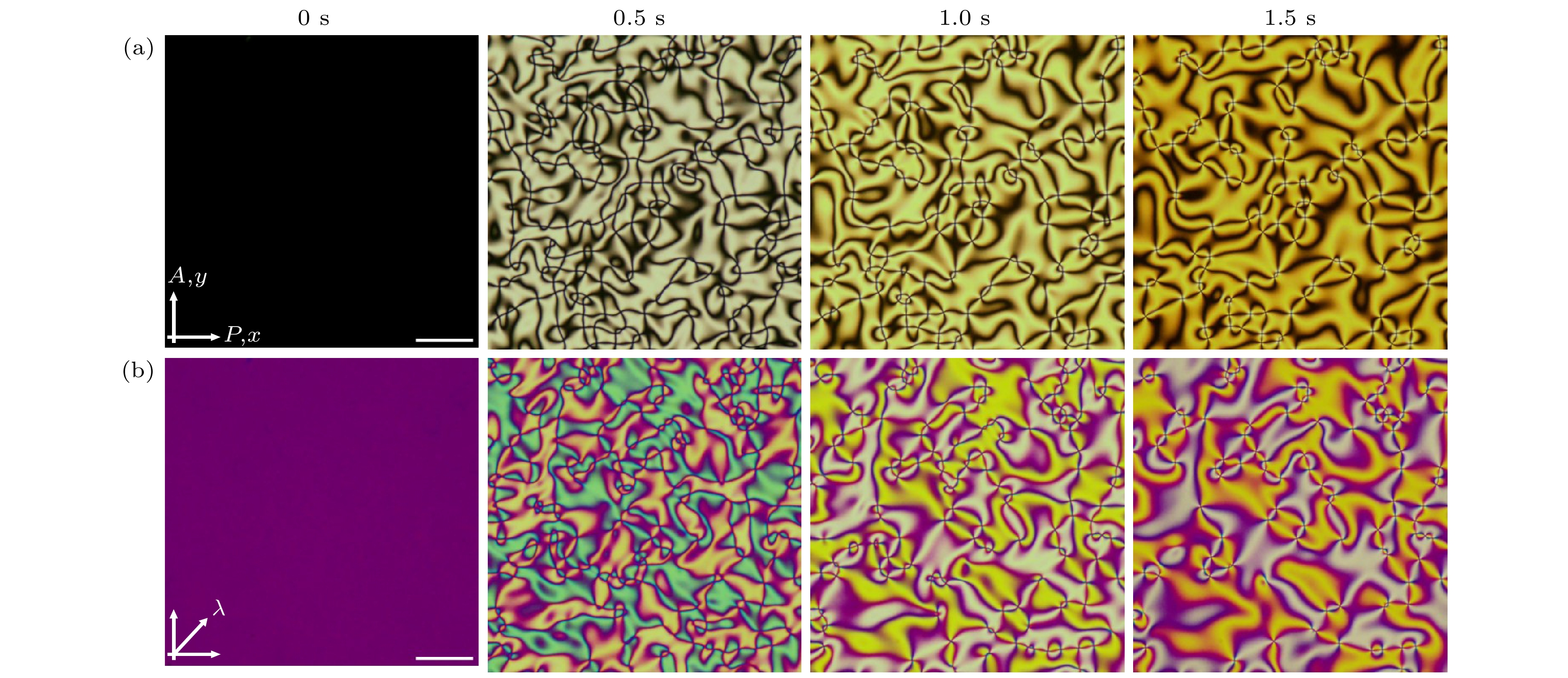
图 2 不同时刻t = 0, 0.5, 1.0, 1.5 s下, 电场作用下脐点缺陷产生的POM图像 (a) 正交偏振片下; (b) 插入全波片(波长为530 nm). 材料: H4, 电压变化率为1.0 V/s, 工作温度T = 25 ℃, 频率$f = {\text{1 kHz}}$, 盒厚$d = {7}{\text{.6 μm}}$. 比例尺: ${\text{100 μm}}$
Figure 2. POM images of umbilic defects formation under applied electric field at t = 0, 0.5, 1.0, 1.5 s. POM image: (a) With crossed polarizers; (b) a full wave plate of wavelength 530 nm. Material is H4, electric field ramp rate is 1.0 V/s, the working temperature is T = 25 ℃, frequency f = 1 kHz, cell gap $d = {7}{\text{.6 μm}}$. Scale bar: ${\text{100 μm}}$.
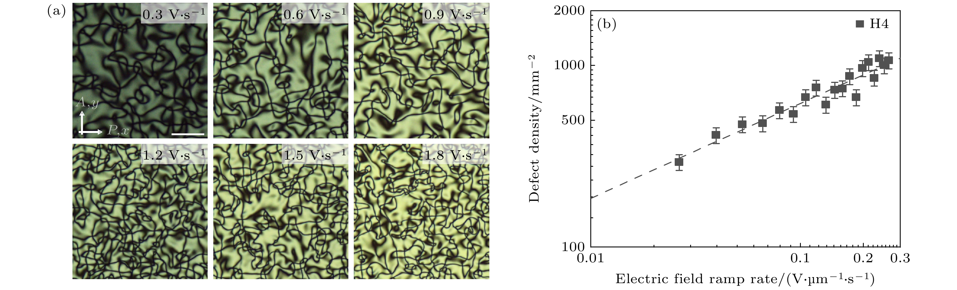
图 3 (a)不同电场变化率下, $ t = {0}{\text{.3 s}} $时刻下产生的脐点缺陷的POM图像, 每张图像素大小$ {\text{1488 pixel}} \times {\text{1500 pixel}} $, 实际对应尺寸为$ {\text{551 μm}} \times {\text{556 μm}} $; (b)电场变化率与缺陷密度的关系, 虚线为线性拟合. 液晶材料: H4, 工作温度T = 25 ℃, 频率$ f = {\text{1 kHz}} $, 盒厚$d = {7}{\text{.6 μm}}$, 比例尺: $ {\text{100 μm}} $
Figure 3. (a) POM image of umbilic defects generated at different electric field ramp rate over a time period of 0.3 s. Each image size is $ {\text{1488 pixel}} \times {\text{1500 pixel, }} $ corresponding to $ {\text{551 μm}} \times {\text{556 μm}} $. (b) The relationship between electric field ramp rate and the defects density. The dashed lines represent the linear fitting. Material: H4, the working temperature of T = 25 ℃, frequency of $ f = {\text{1 kHz}} $, cell gap of $d = {7}{\text{.6 μm}}$. Scale bar: $ {\text{100 μm}} $.

图 4 (a) 4种液晶材料H1, H3, H4和H7电场变化率与缺陷密度关系; (b) 7种不同负介电各向异性$\Delta \varepsilon $与标度指数$\alpha $和截距b值的依赖关系. 虚线为线性拟合. 液晶材料: H1, H2, H3, H4, H5, H6和H7. 工作温度T = 25 ℃, 频率$f = {\text{1 kHz}}$
Figure 4. (a) The relationship between defect density and the electric field ramp rate for four liquid crystals materials: H1, H3, H4 and H7; (b) the dependence of the scaling exponent $\alpha $ and b on the seven negative dielectric anisotropy $\Delta \varepsilon $. The dashed lines represent the linear fitting. The liquid crystals: H1, H2, H3, H4, H5, H6 and H7. The working temperature is T = 25 ℃, frequency $f = {\text{1 kHz}}$.

图 5 (a)—(c)不同温度$ T $下, 缺陷密度和电场变化率的关系; (d)标度指数$\alpha $与温度$ T - {T_{{\text{NI}}}} $的依赖关系. 虚线为线性拟合. 三种液晶材料: H1($ d = {8}{\text{.8 μm}} $), H4: ($ d = {7}{\text{.6 μm}} $), H7: ($ d = {8}{\text{.3 μm}} $), 工作温度$ T={T}_{\text{NI}}-40 $ ℃, ${T}_{\text{NI}}-30 $ ℃, ${T}_{\text{NI}}-20 $ ℃, 频率$f = {\text{1 kHz}}$
Figure 5. (a)–(c) The relationship between defect density and the electric field ramp rate at different temperatures $ T $; (d) the dependence of the scaling exponent $\alpha $ on reduced temperature $ T - {T_{{\text{NI}}}} $. The dashed lines represent the linear fitting. The three liquid crystals: H1($ d = {8}{\text{.8 μm}} $), H4 ($ d = {7}{\text{.6 μm}} $), H7 ($ d = {8}{\text{.3 μm}} $), the working temperature is $ T={T}_{\text{NI}}-40 $ ℃, ${T}_{\text{NI}}-30 $ ℃, ${T}_{\text{NI}}-20 $ ℃, frequency $f = {\text{1 kHz}}$

图 6 (a)—(c)不同频率$f$下, 缺陷密度和电场变化率的关系; (d)标度指数$\alpha $与频率$f$的依赖关系. 虚线为线性拟合. 三种液晶材料: H1($d = {8}{\text{.8 μm}}$), H4($d = {7}{\text{.6 μm}}$), H7($d = {8}{\text{.3 μm}}$), 工作温度$T =25 $ ℃
Figure 6. (a)–(c) The relationship between defect density and the electric field ramp rate at different frequency $f$; (d) the dependence of the scaling exponent $\alpha $ on the frequency $f$of the electric field. The dashed lines represent the linear fitting. The three liquid crystals: H1($d = {8}{\text{.8 μm}}$), H4 ($d = {7}{\text{.6 μm}}$), H7 ($d = {8}{\text{.3 μm}}$). The working temperature is $T =25 $ ℃
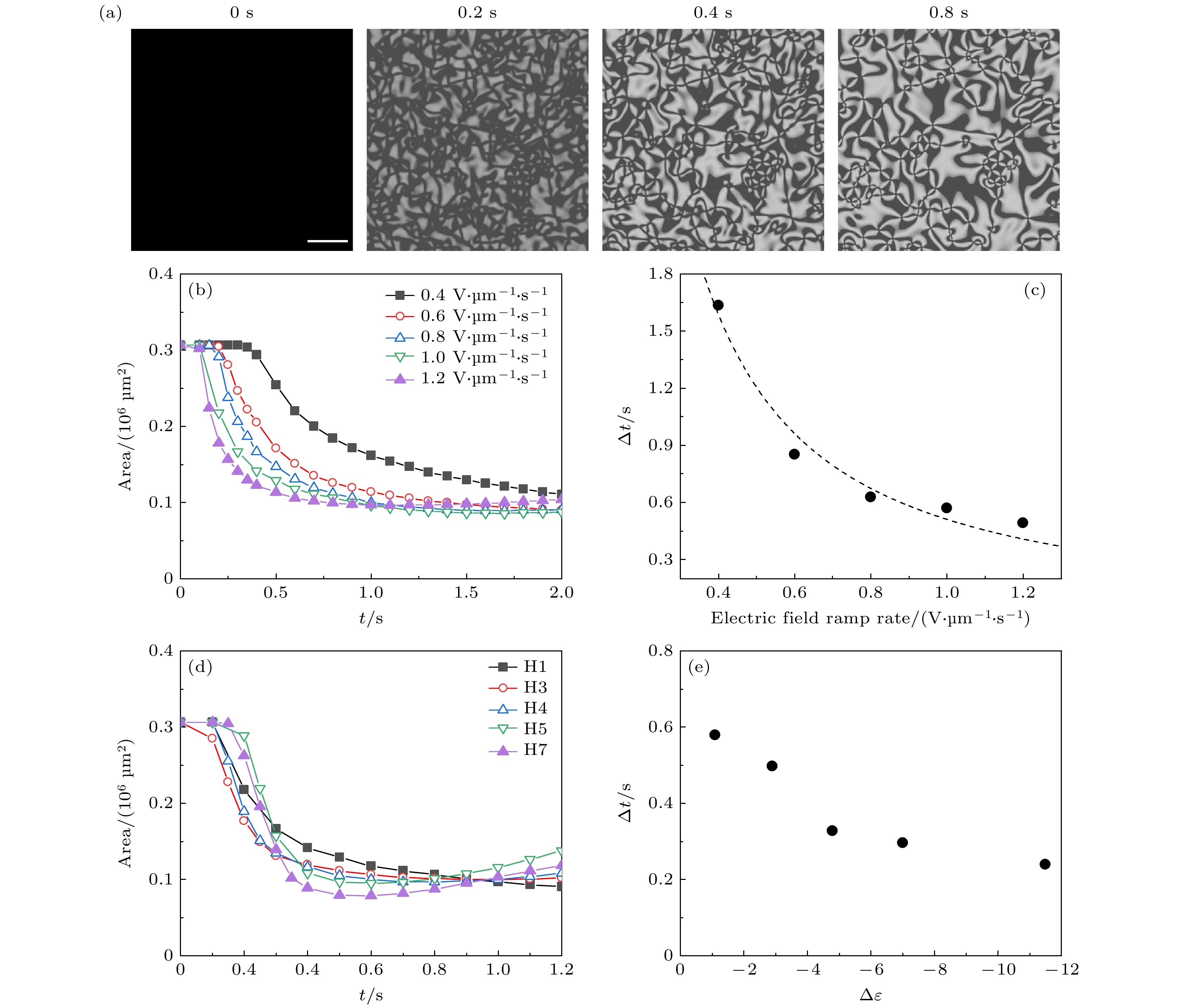
图 7 (a)不同时刻$ t = {\text{0 , }} {\text{0.2, 0}}{\text{.4, 0}}{\text{.8 s}}$, 经ImageJ二值化处理后的脐点缺陷时间序列图, 比例尺: ${\text{100 μm}}$. 液晶材料H1在0.4, 0.6, 0.8, 1.0, 1.2 V/s电场变化率下 (b) ${S_{\text{a}}}$与时间$t$关系; (c) 电压变化率与缺陷湮灭特征时间$\Delta t$的依赖关系. 虚线为$\Delta t \propto $$ \tau _{\text{C}}^{{{ - 1}}{.2}}$. 液晶材料H1, H3, H4, H5和H7, 在电场变化率为1.0 V/s时, (d) ${S_{\text{a}}}$与时间$t$关系, 以及(e)介电各向异性$\Delta \varepsilon $与缺陷湮灭特征时间$\Delta t$的依赖关系. 工作温度$T = $ 25 ℃, 频率$f = {\text{1 kHz}}$
Figure 7. (a) POM images of umbilic defects at different moments after binarization processed by ImageJ, $ t {\text{ = 0, 0}}{\text{.2, 0}}{\text{.4, 0}}{\text{.8 s}} $, scale bar: ${\text{100 μm}}$; (b) the relationship between the time $t$ and ${S_{\text{a}}}$, and (c) the dependence of the annihilation time $\Delta t$ at the electric field ramp rate of 0.4, 0.6, 0.8, 1.0, 1.2 V/s for H1. The dashed line represents $\Delta t \propto \tau _{\text{C}}^{{{ - 1}}{.2}}$. (d) The relationship between the time and ${S_{\text{a}}}$, and (e) the dependence of the annihilation time $\Delta t$on the dielectric anisotropy $\Delta \varepsilon $ at the electric field ramp rate of 1.0 V/s for H1, H3, H4, H5 and H7. The working temperature $T = $ 25 ℃, frequency $f = {\text{1 kHz}}$.
表 1 7种负介电各向异性向列相液晶材料的物理特性.
Table 1. Physical properties of seven nematic liquid crystals with negative dielectric anisotropy.
简称 液晶材料 $\Delta \varepsilon $(25 ℃,
1 kHz)$\Delta n$($\lambda = $ $ {\text{589 nm}}$) TNI/℃ H1 HNG723200-000 –1.1 0.071 70 H2 HNG733300-000 –2.0 0.078 100 H3 HNG715800-000 –2.9 0.074 88 H4 HNG736600-000 –4.8 0.080 95 H5 HNG735200-000 –7.0 0.088 96 H6 HNG715700-000 –8.1 0.075 87 H7 HNG725100-100 –11.5 0.077 77  DownLoad: CSV
-
[1] Li J, Bisoyi H K, Tian J, Guo J, Li Q 2019 Adv. Mater. 31 1807751
Google Scholar
[2] Wang J W, Li K, He H I, Cai W F, Liu J X, Yin Z, Mu Q Q, Hisao V K S, Gérard D, Luo D, Li G, Liu Y J 2022 Laser Photonics Rev. 16 2100396
Google Scholar
[3] Yang C, Wu B, Ruan J, Zhao P, Chen L, Chen D, Ye F 2021 Adv. Mater. 33 2006361
Google Scholar
[4] Li X, Ma S, Hu J, Ni Y, Lin Z, Yu H 2019 J. Mater. Chem. C 7 622
Google Scholar
[5] Hu J, Yu M, Wang M, Choy K L, Yu H 2022 ACS Appl. Mater. Interfaces 14 12951
Google Scholar
[6] Ji Z C, Zhang X Z, Zhang Y J, Wang Z H, Drevensek-Olenik I, Rupp R, Li W, Wu Q, Xu J J 2017 Chin. Opt. Lett. 15 070501
Google Scholar
[7] 王磊, 肖芮文, 葛士军, 沈志雄, 吕鹏, 胡伟, 陆延青 2019 物理学报 68 084205
Google Scholar
Wang L, Xiao R W, Ge S J, Shen Z X, Lü P, Hu W, Lu Y Q 2019 Acta Phys. Sin. 68 084205
Google Scholar
[8] 朱雨雯, 袁丛龙, 刘炳辉, 王骁乾, 郑致刚 2019 物理学报 72 174206
Google Scholar
Zhu Y W, Yuan C L, Liu B H, Wang X Q, Zheng Z G 2019 Acta Phys. Sin. 72 174206
Google Scholar
[9] Zurek WH 1985 Nature 317 505
Google Scholar
[10] Kibble TWB 1976 J. Phys. A: Math. Gen. 9 1387
Google Scholar
[11] del Campo A, Zurek WH 2014 Int. J. Mod. Phys. A 29 1430018
Google Scholar
[12] 张馨元, 崔慧林, 王钰, 陈宏一, 张心正 2022 液晶与显示 37 1032
Google Scholar
Zhang X Y, Cui H L, Wang Y, Chen H Y, Zhang X Z 2022 Chin. J. Liq. Cryst. Disp. 37 1032
Google Scholar
[13] Ohzono T, Katoh K, Wang C, Fukazawa A, Yamaguchi S, Fukuda J 2017 Sci. Rep. 7 16814
Google Scholar
[14] Rapini A 1973 J. Phys. France. 34 629
Google Scholar
[15] Wu S B, Wu J B, Cao H M, Lu Y Q, Hu W 2023 Phys. Rev. Lett. 130 078101
Google Scholar
[16] Fumeron S, Berche B 2023 Eur. Phys. J. Spec. Top. 232 1813
Google Scholar
[17] de Oliveira B F, Avelino P P, Moraes F, Oliveira J C R E 2010 Phys. Rev. E 82 041707
Google Scholar
[18] Shen Y, Dierking I 2019 Soft Matter 15 8749
Google Scholar
[19] Pismen LM, Rubinstein BY 1992 Phys. Rev. Lett. 69 96
Google Scholar
[20] Williams C, Pierański P, Cladis P E 1972 Phys. Rev. Lett. 29 90
Google Scholar
[21] Chuang I, Turok N, Yurke B 1991 Phys. Rev. Lett. 66 2472
Google Scholar
[22] Osterman N, Kotar J, Terentjev E M, Cicuta P 2010 Phys. Rev. E 81 061701
Google Scholar
[23] Harth K, Stannarius R 2020 Front. Phys. 8 112
Google Scholar
[24] Zhang Y H, Deserno M, Tu Z C 2020 Phys. Rev. E 102 012607
Google Scholar
[25] Grollau S, Abbott N L, de Pablo J J 2003 Phys. Rev. E 67 051703
Google Scholar
[26] Svenšek D, Žumer S 2002 Phys. Rev. E 66 021712
Google Scholar
[27] Bogi A, Martinot-Lagarde P, Dozov I, Nobili M 2002 Phys. Rev. Lett. 89 225501
Google Scholar
[28] Oswald P, Ignés-Mullol J 2005 Phys. Rev. Lett. 95 027801
Google Scholar
[29] Zurek WH 1996 Phys. Rep. 276 177
Google Scholar
[30] Dziarmaga J 2010 Adv. Phys. 59 1063
Google Scholar
[31] Kleman M, Lavrentovich OD 2006 Philos. Mag. 86 4117
Google Scholar
[32] Chuang I, Durrer R, Turok N, Yurke B 1991 Science 251 1336
Google Scholar
[33] Dierking I, Marshall O, Wright J, Bulleid N 2005 Phys. Rev. E 71 061709
Google Scholar
[34] Dierking I, Ravnik M, Lark E, Healey J, Alexander GP, Yeomans J M 2012 Phys. Rev. E 85 021703
Google Scholar
[35] Fowler N, Dierking I 2017 ChemPhysChem 18 812
Google Scholar
[36] Nagaya T, Hotta H, Oriharaand Yoshihiro Ishibashi H 1992 J. Phys. Soc. Jpn. 61 3511
Google Scholar
[37] Toyoki H 1990 J. Phys. Rev. A 42 911
Google Scholar


 DownLoad:
Catalog
Metrics
- Abstract views: 745
- PDF Downloads: 40
- Cited By: 0
