


INVITED REVIEW
INVITED REVIEW
2020, 69 (15): 154301.
doi: 10.7498/aps.69.20200406
Abstract +
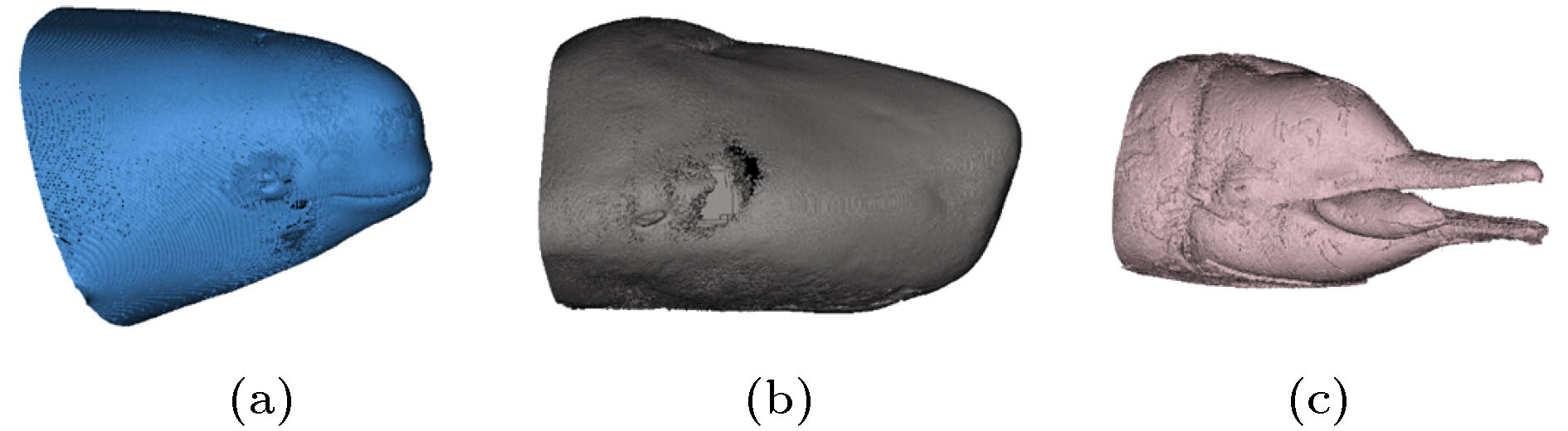
Odontocetes have evolved for millions of years to own a unique echolocation system. The exceptional performance of odontocetes echolocation system can provide reference to artificial sonar systems, acoustic metamaterials and sound control designs. Research on odontocetes biosonar requires interdisciplinary effort, including acoustics, biology, biomimetics, anatomy, physiology and signal analysis. In this paper, we review odontoctes’ biosonar emission process from aspects of anatomy, biosonar signal and beam formation. To begin, computed tomography scanning and untrasound measurements are combined to reconstruct the sound speed and density distributions. To follow, efforts are thrown to probe into the biosonar signal and its corresponding acoustic behavior. Numerical simulations are used to investigate the odontocetes’ biosonar beam formation. The secret of exceptional performance of odontocetes’ echolocation system lies in their unique anatomy. Odontocete integrates acoustic structures with different acoustic impedances, namely solid bony structures, air space and soft tissues as a whole emission system to efficiently modulate sound propagation and sound beam formation. These acoustic structures are well organized in the forehead, forming a natural acoustic metamaterial to perform a good control of sounds. These results can enlighten artificial sonar designs.

SPECIAL TOPIC—Optical metamaterials
2020, 69 (15): 150301.
doi: 10.7498/aps.69.20200258
Abstract +
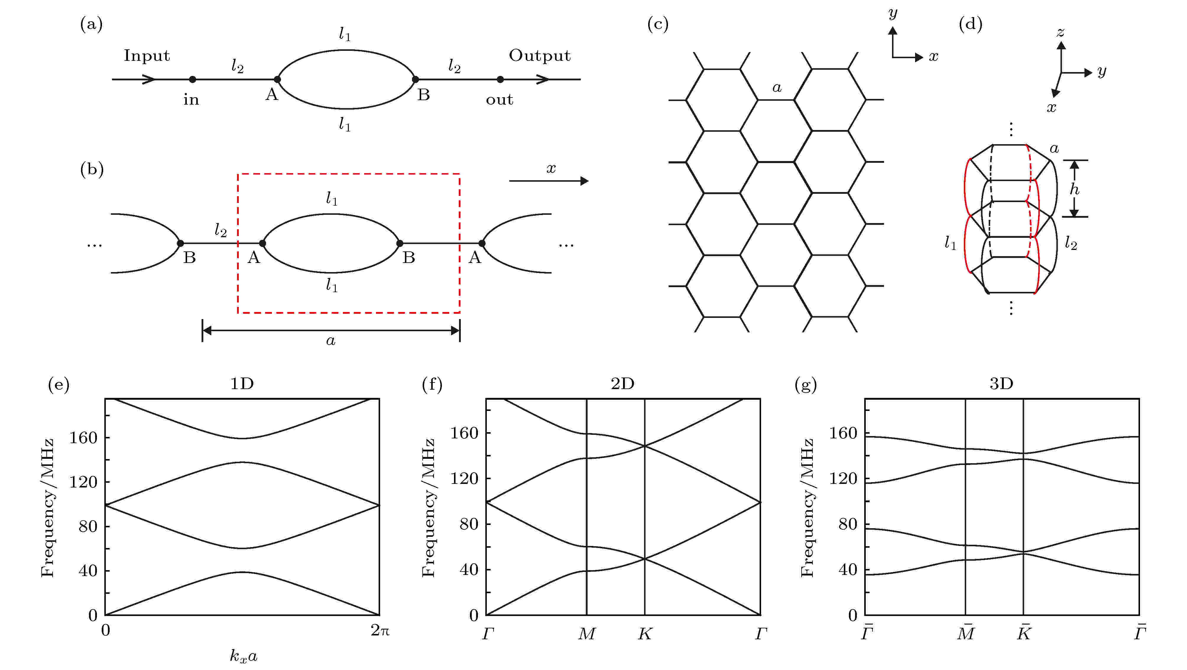
Transmission line is a common kind of one-dimensional waveguide. In addition to being widely used in engineering, the transmission lines can be used in proof-of-principle experiments in basic scientific research. For example, the wave equations governing the transmission line and quantum wire are equivalent, so transmission lines are widely used in the research of quantum graphs. The transmission line network equations are similar to the equations of zero-energy tight binding model, so the transmission line network can also be used to study some physical properties predicted by the theories based on tight binding model, and examples include Anderson localization, band dispersions, topological properties, etc. According to the transmission line network equations, we review some applications of transmission lines in the research fields mentioned above. We will discuss Anderson localization in one-, two-, and three-dimensional networks, the band structures of periodic and quasiperiodic networks, and the angular moment-dependent topological transport in transmission line network. We introduce the methods and results in detail to show the potential of transmission lines in basic scientific research.
2020, 69 (15): 154103.
doi: 10.7498/aps.69.20200260
Abstract +
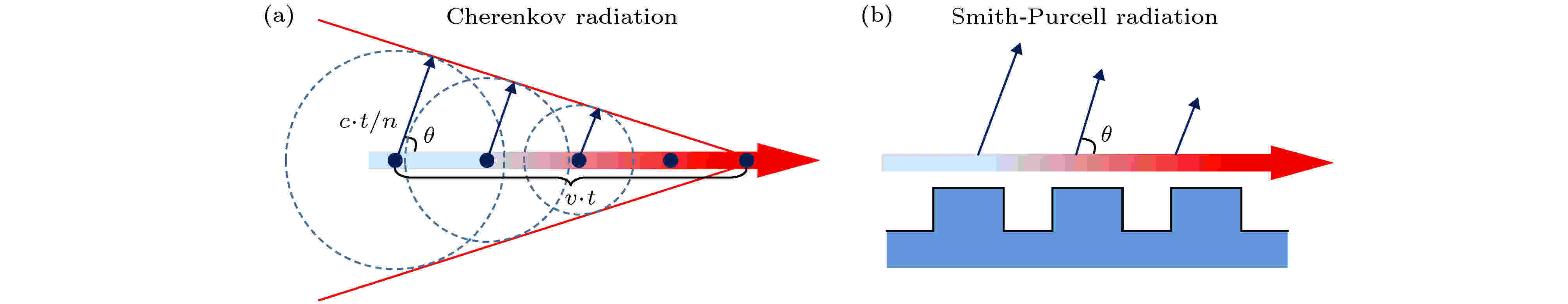
Cherenkov radiation (CR) is an electromagnetic radiation emitted by charged particles traveling through a dielectric medium at a speed faster than the phase velocity of light. CR plays an important role in the fields of particle detection, biomedicine and electromagnetic-radiation source. Recently, metamaterials demonstrate their novel mechanical, acoustic, and optical properties by delicately designing the structures and materials. In metamaterials, the electromagnetic properties, such as wave propagation, coupling, and radiation, could be flexibly manipulated. Thus, it is expected that the combination of vacuum electronics and micro- & nano-photonics would result in numerous novel phenomena and effects by having free electrons interacting with metamaterials. In this paper, we firstly review the concept and generation mechanism of CR. Then, recent research advances in the CR generation by using different types of metamaterials are reviewed, including threshold-less CR in hyperbolic metamaterials, reverse CR in negative metamaterials, CR lasing based on high Q-factor metamaterials and Smith-Purcell radiation manipulation with metasurfaces. The unique characteristics and interesting mechanisms of CR based on these metamaterials are elaborated. The research and development of interaction between free electrons and various metamaterials open up possibilities for realizing novel integrated free-electron devices.

2020, 69 (15): 154104.
doi: 10.7498/aps.69.20200976
Abstract +
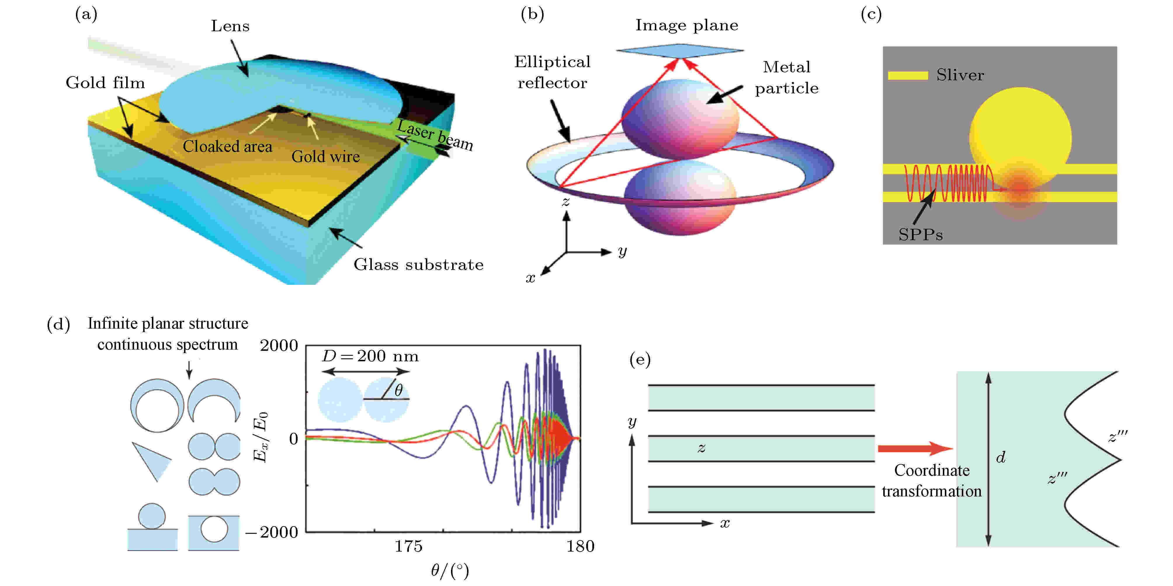
With the development of science and technology, the invisibility has gradually moved from a simple and plain visual deception trick to a precise and systematic modern technology system. By designing appropriate electromagnetic parameters, the novel electromagnetic wave cloaking technology is able to control the propagation and scattering of electromagnetic wave, thereby reducing the detectability of the cloaked object. The electromagnetic parameters of these novel cloaking devices can be realized by using the artificially designed nanostructures, or by combining the medium that already exists in nature. In this review, according to a detailed introduction of the research progress of novel electromagnetic wave cloaking, we discuss the difficulties and challenges in this field, and give an outlook on the future development.

2020, 69 (15): 154202.
doi: 10.7498/aps.69.20200453
Abstract +
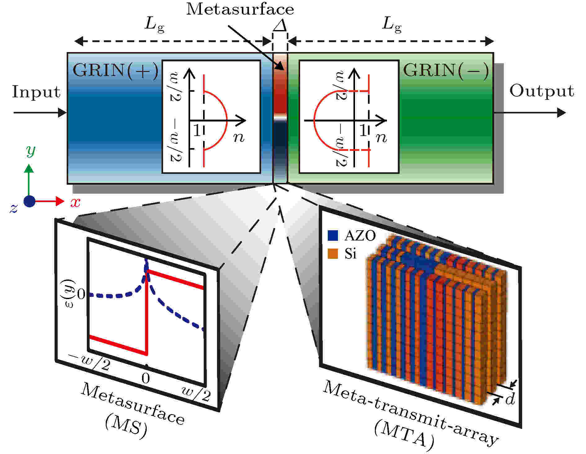
Due to their superior ability to control light, metasurfaces, ultrathin two-dimensional metamaterials composed of subwavelength nanostructures, have attracted great attention in recent years. Exploring geometric and material freedom in designing elementary nanostructures and their ambient environment of metasurfaces enables versatile optical devices, such as planar metalenses, holographic imaging and thermal radiators. With phase-change materials (PCMs) such as GeSbTe and VO2 integrated into metasurfaces, the optical functionalities of metasurfaces can be flexibly tuned by exploiting the phase transitions of PCMs induced by external stimuli, thereby opening up new directions and perspectives for dynamic tunable metamasurfaces. In this article, we review the recent progress of tunable metasurfaces based on PCMs, analyze their underlying working mechanisms and highlight their important applications. We conclude this review by bringing our perspectives on challenges and future directions in this field.
2020, 69 (15): 154205.
doi: 10.7498/aps.69.20200084
Abstract +
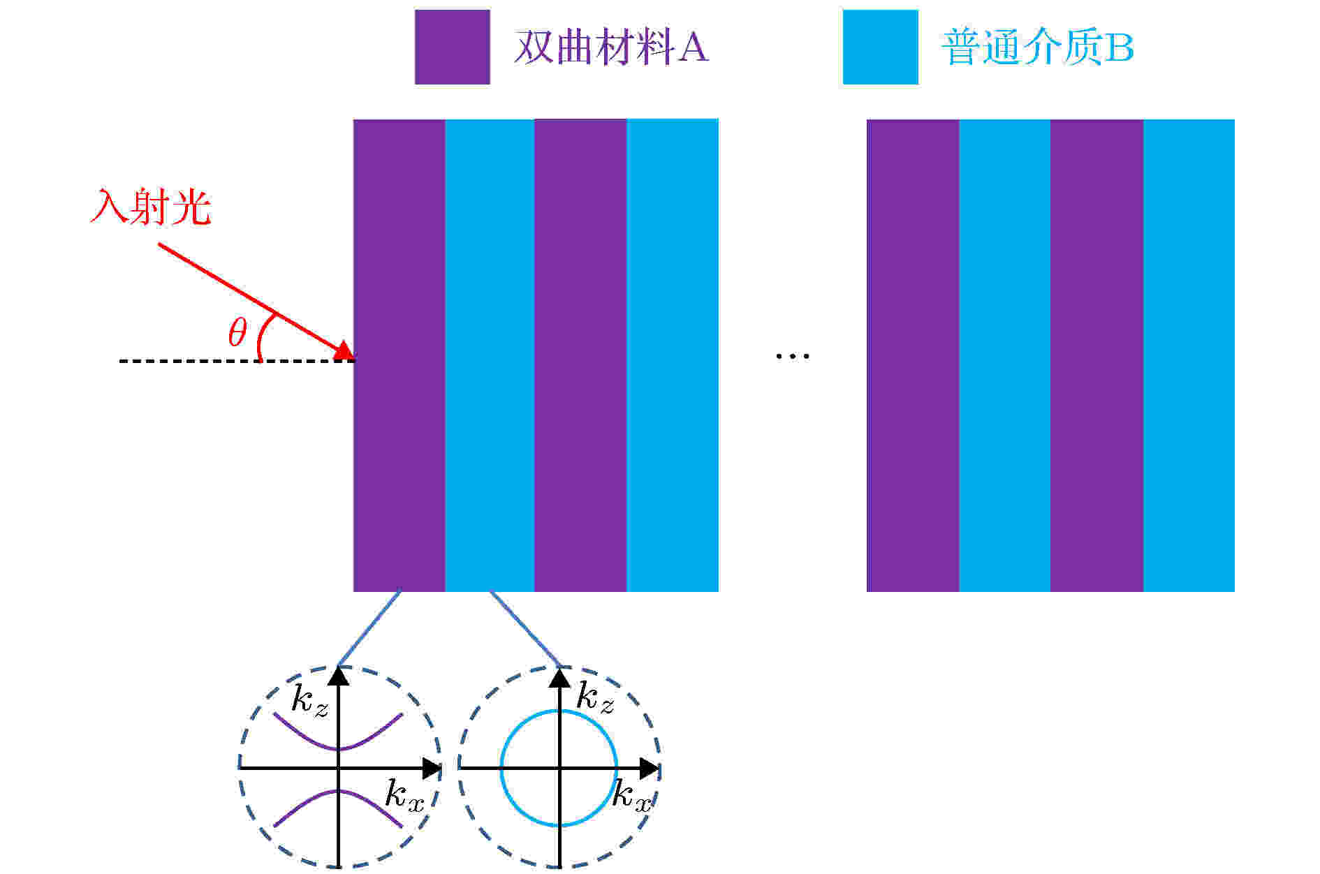
Behaviours of light in materials strongly depend on the topological structure of the iso-frequency surface (IFS). The usual materials, of which the unit cell of photonic crystal is made up, are dielectrics, whose IFSs have the same closed topological structure. As a simplest photonic crystal, one-dimensional photonic crystal (1DPC) has attracted intensive attention due to its simple fabrication technique as well as numerous applications. However, in a conventional all-dielectric 1DPC, photonic band gaps (PBGs) for both transverse magnetic (TM) and transverse electric (TE) polarizations will shift toward short wavelengths (i.e. blueshift) as incident angle increases. The underlying physical reason is that the propagating phase in isotropic dielectric will decrease as incident angle increases. The blueshift property of band gap for TM and TE polarization will limit the band width of omnidirectional band gap and the range of operating incident angles in some PBG-based applications, including near-perfect absorption, polarization selection and sensitive refractive index sensing. However, for TM polarization, the propagating phase in a hyperbolic metamaterial (HMM) will increase with incident angle increasing. This special phase property of HMM provides us with a way to flexibly tune the angle-dependent property of band gap in periodic compound structure composed of alternative HMM with open IFS and dielectric with close IFS. In this review, we realize zeroshift (i.e. angle-independent) band gaps as well as redshift band gaps in 1DPCs containing HMMs, which can be utilized to realize near-perfect absorption, sensitive refractive index sensing and polarization selection working in a wide range of incident angles.
2020, 69 (15): 154206.
doi: 10.7498/aps.69.20200194
Abstract +
Mode coupling is a common phenomenon in waveguides. The mode coupling among different guided modes in fiber-optic communication can cause crosstalk, and the mode coupling of guided mode and radiated mode can reduce the power of the guided mode. Application of mode coupling can guide the design of optical devices such as couplers and beam splitters with specific functions, which have been widely used in fiber optic communication and fiber sensing. So it is important to analyze how waveguide modes are coupled. The coupled-mode theory is a common method of studying mode coupling in waveguides. It provides not only an intuitive picture of how the photonic modes are hybridized, but also a quantitative assessment of how the hybridization among those relevant modes evolves. In recent years, non-Hermitian waveguides, represented by parity-time symmetrical structures, have become a research hotspot. However the conventional coupled-mode theory no longer works in this case. In this review, we briefly summarize the development history of coupled-mode theory and introduce the representative work in reciprocal waveguide coupled-mode theory in detail. Then the relationship among several coupled-mode theories is analyzed and their applications are briefly introduced.
2020, 69 (15): 154207.
doi: 10.7498/aps.69.20200384
Abstract +
In recent years, flatband systems have aroused considerable interest in different branches of physics, from condensed-matter physics to engineered flatband structures such as in ultracold atoms, various metamaterials, electronic materials, and photonic waveguide arrays. Flatband localization, as an important phenomenon in solid state physics, is of broad interest in the exploration of many fundamental physics of many-body systems. We briefly review the recent experimental advances in light localization in engineered flatband lattices, with the emphasis on the optical induction technique of various photonic lattices and unconventional flatband states. The photonic lattices, established by various optical induction techniques, include quasi-one-dimensional diamond lattices and two-dimensional super-honeycomb, Lieb and Kagome lattices. Nontrivial flatband line states, independent of linear superpositions of conventional compact localized states, are demonstrated in photonic Lieb and super-honeycomb lattices, and they can be considered as an indirect illustration of the non-contractible loop states. Furthermore, we discuss alternative approaches to directly observing the non-contractible loop states in photonic Kagome lattices. These robust loop states are direct manifestation of real-space topology in such flatband systems. In this paper we do not intend to comprehensively account the vast flatband literature, but we briefly review the relevant work on photonic lattices mainly from our group. We hope that the mentioned concepts and techniques can be further explored and developed for subsequent applications in other structured photonic media such as photonic crystals, metamaterials, and other synthetic nanophotonic materials.
2020, 69 (15): 157301.
doi: 10.7498/aps.69.20200193
Abstract +
Due to its special optical properties the surface plasmon polariton (SPP) has been applied to many fields such as chemistry, biology, communication, nano energy. The more in-depth researches on plasmonic band structures can conduce to understanding more the properties of plasmonic micro- and nano-structures. In this review, we first introduce some metal structures which have plasmonic band structures. Then, we review some unique properties of plasmonic band structures including bound state in the continuum, waveguide, complete band gap, topology, etc. Based on the above properties, the plasmonic applications are introduced. Finally, we briefly introduce the band structures of graphene-based plasmonics and its applications.
2020, 69 (15): 157802.
doi: 10.7498/aps.69.20200183
Abstract +
Optical metamaterial is a kind of artificially designed microstructured material. Its occurrence breaks the localization of traditional material design thinking and provides a new paradigm for artificially controlling electromagnetic waves on a micro-nano scale, especially realizes optical properties beyond conventional materials in nature. Furthermore, metamaterial has the ability to couple electromagnetic waves into the sub-wavelength regime, meeting the high-speed development of modern science and technology, which puts forward new requirements for high performance, miniaturization and integration of optical components. Therefore, optical chips based on metamaterials bring many encouraging applications such as in perfect imaging that breaks through the diffraction limit, multifunctional integrated optics, etc. In addition, metamaterial photonic chips can also simulate some phenomena in general relativity, especially exploring some phenomena that have not been experimentally proven. This review paper briefly introduces the study of analogical gravitation based on different kinds of photonic chips on the basis of metamaterials. In the end, there present the summary and outlook about the current development, advantages and challenges of this field.
2020, 69 (15): 157803.
doi: 10.7498/aps.69.20200283
Abstract +
Spatial analog optical computing devices possess the capability of high-throughput, real-time and low-energy information processing. Optical metamaterials, which are ultracompact in structure and possess powerful ability to control the light, can be utilized to establish miniatured and integrated spatial analog optical computing devices. The methods of designing the spatial analog optical computing devices could be mainly classified as two kinds—4F system method and Green’s function method. The 4F system method requires two Fourier transform lenses and a spatial frequency filter, where the actual computing procedure is performed in the spatial domain. The 4F system is usually bulky and complicated. The Green’s function method directly leverages the nonlocal response of the carefully tailored optical materials to implement analog computing procedure in the spatial frequency domain and its structure is compact without extra Fourier transform components. Research advances in spatial analog optical computing devices by using these two methods for the last few years are introduced in this paper. These researches could be classified as differentiators, integrators, equation solvers and spatial frequency filters according to the standard of computing functions. The approaches to designing these devices are further demonstrated. Then, computing devices which could realize spatial analog first-order difference by use of the spin-orbit interaction proposed recently are introduced. Finally, application fields and study prospects of spatial analog optical computing devices are discussed and summarized.
2020, 69 (15): 157804.
doi: 10.7498/aps.69.20200614
Abstract +
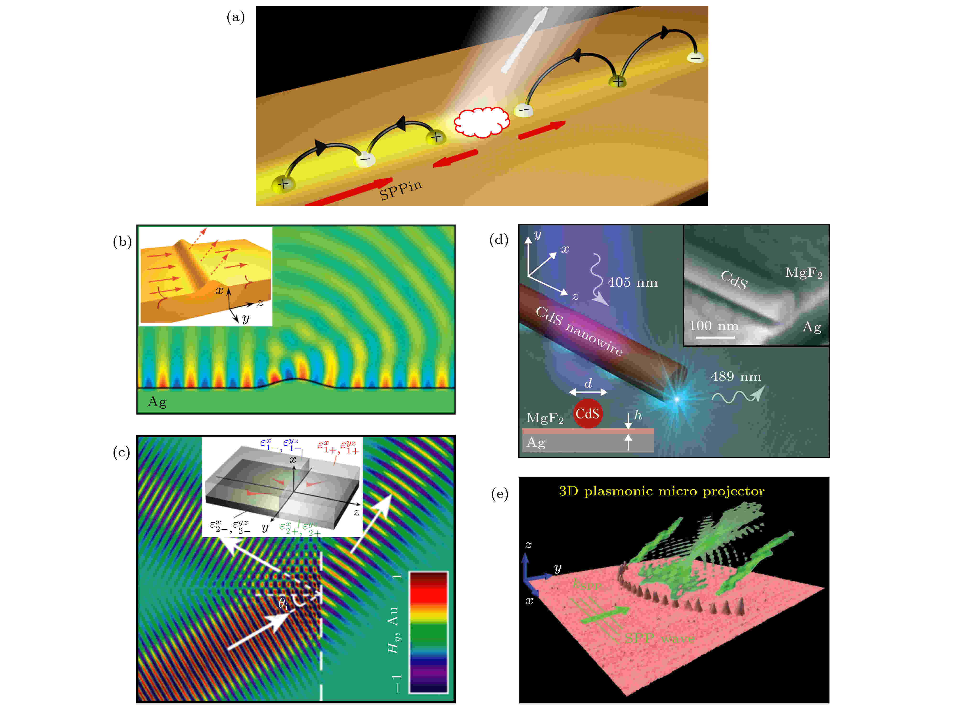
Surface plasmon polaritons (SPPs) have found many important applications in on-chip signal transportation, enhanced nonlinear/Raman effect, biological/chemical sensing, super resolution imaging, etc. In these applications, the near-field propagation and far-field scattering of SPPs play a vital role. However, there has been strong desire to understand these physical effects. In this paper, we first briefly review the history and progress of SPPs. Next, we mainly focus on the near-field propagation and far-field scattering of SPPs, including their fundamental theories and practical applications. Finally, we review several different approaches to manipulating the near-field wavefronts of SPPs. These researches offer us a more in-depth understanding and the ability to more strongly control the scattering characteristics of SPPs, which may promote the scientific researches and practical applications of SPPs in the future.
2020, 69 (15): 158101.
doi: 10.7498/aps.69.20200246
Abstract +
2020, 69 (15): 154101.
doi: 10.7498/aps.69.20200147
Abstract +
Field enhancement is an interesting and important topic in electromagnetic study. Electromagnetic field concentration and enhancement devices have wide applications in high directional antenna design, laser ignition, optical control, etc. At present, there are usually two ways of implementing the field enhancement, one is to use the artificial electromagnetic materials to realize the radiation direction control and energy concentration, which is more suitable for the applications at microwave or lower frequencies, and the other is to use the materials with high permittivity or high permeability. However, the latter is extremely sensitive to the position and characteristic of the radiation source and the cross-sectional area of the material, and depends heavily on the value of the relative permittivity or the relative permeability of the material. Therefore, both methods cannot fully meet the application requirements of creating high field intensity in optical band, such as laser ignition, etc. In this paper, based on the theory of photonic crystal doping, the strong electromagnetic field enhancement has been successfully realized by epsilon-near-zero medium filled with ordinary dielectric dopant. We first make the comprehensive theoretical analysis of the field enhancement in the structure of epsilon-near-zero medium with dielectric dopant. The method of calculating the central magnetic field in the doped medium is then rigorously derived, and the formula for the ratio of the central magnetic field in the doped medium to the external radiation field is deduced. We find that the optimal magnetic field enhancement occurs only when the proposed structure is equivalent to an epsilon-mu-near-zero medium. Subsequently, under the above condition, various parameters (radius of the cylindrical dopant, number of sources, etc.) are studied to analyze the magnetic field enhancement performance inside the doped medium. The theoretical analysis and simulation results show that the proposed structure can significantly enhance the magnetic field which is applicable in a broad frequency band from microwave to optical region, and meets the application requirements of providing high field intensity. Finally, as a practical realization example, an ultraviolet ignition device working at 270 nm is designed, which presents an efficient and alternative way of developing electromagnetic (optical) devices for producing strong field enhancement.

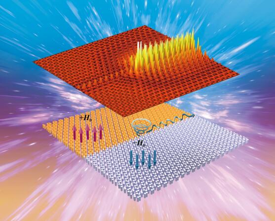
COVER ARTICLE
2020, 69 (15): 154102.
doi: 10.7498/aps.69.20200198
Abstract +
The topological transitions in two-dimensional photonic crystals (PCs) originate from the opening-closing-reopening of the bandgap, accompanied with the band order inversion. The topological bandgap in magnetic PC can be created by applying a bias magnetic field or deforming the geometry structure of the PC. In this paper, we demonstrate that the direction of the bias magnetic field also plays a key role in modifying the band structure in a two-dimensional magnetic PC. The results show that by reversing the direction of the bias magnetic field, the eigenstates with the same parity may exchange their orders in the band structure. We investigate this type of band order exchange in the applications of constructing topological edge states and its influence on the properties of edge states. We find, for example, reversing the direction of the bias magnetic field can create two almost degenerated topological edge modes, which propagate in the same direction but have opposite orbital angular momenta. The edge modes and their characteristics can be determined by the schematics of the band orders for the photonic crystals on the two sides of the boundary. The relative relationship of the band orders determines the emergence of the topological edge states, the number of edge states, and edge modes’ properties such as the orbital angular momentum and group velocity. Also, it affects the transmission efficiency of the electromagnetic wave on the boundary. The direction effect of the bias magnetic field on band order exchange presented in this paper provides us with a new way to change the feature of topological edge states and helps us to better understand the influence of band order on topological phases of photonic crystals. It may have potential applications, such as in pseudo-spin splitter and reflection-free one-way optical switch.
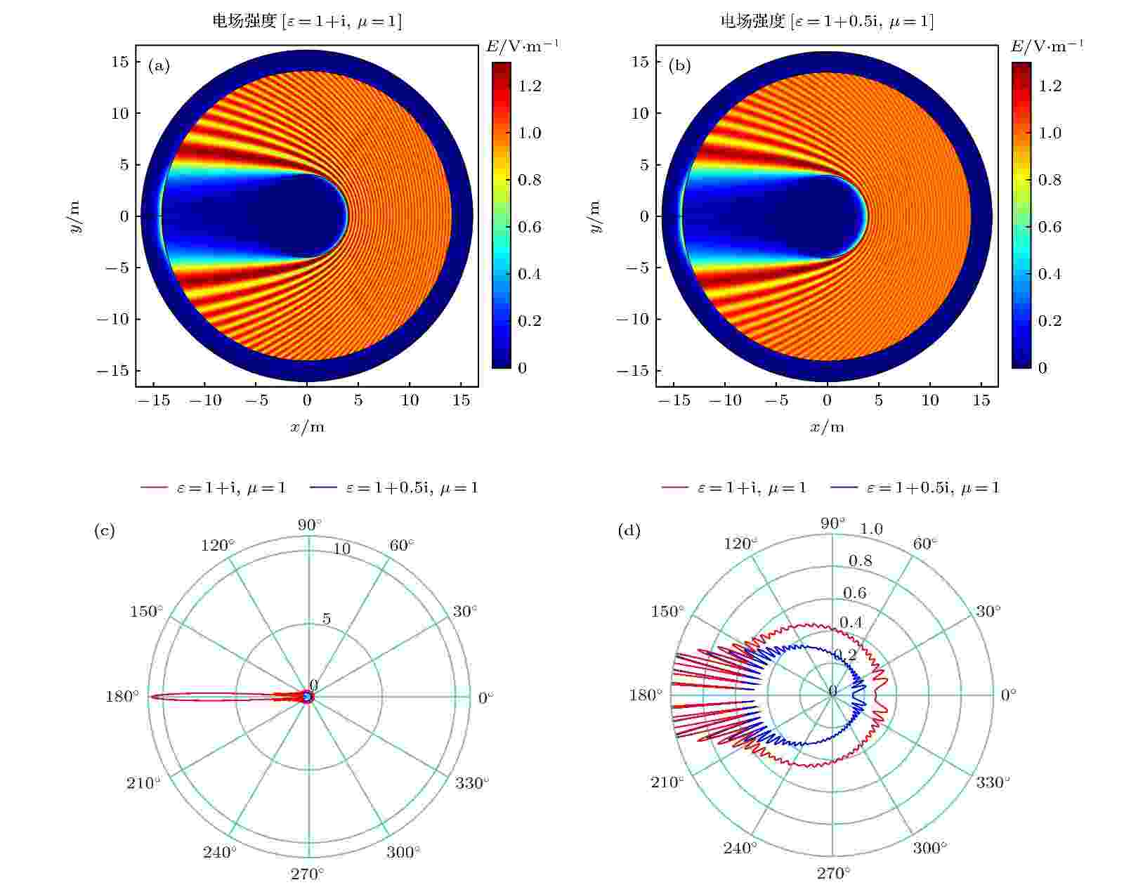
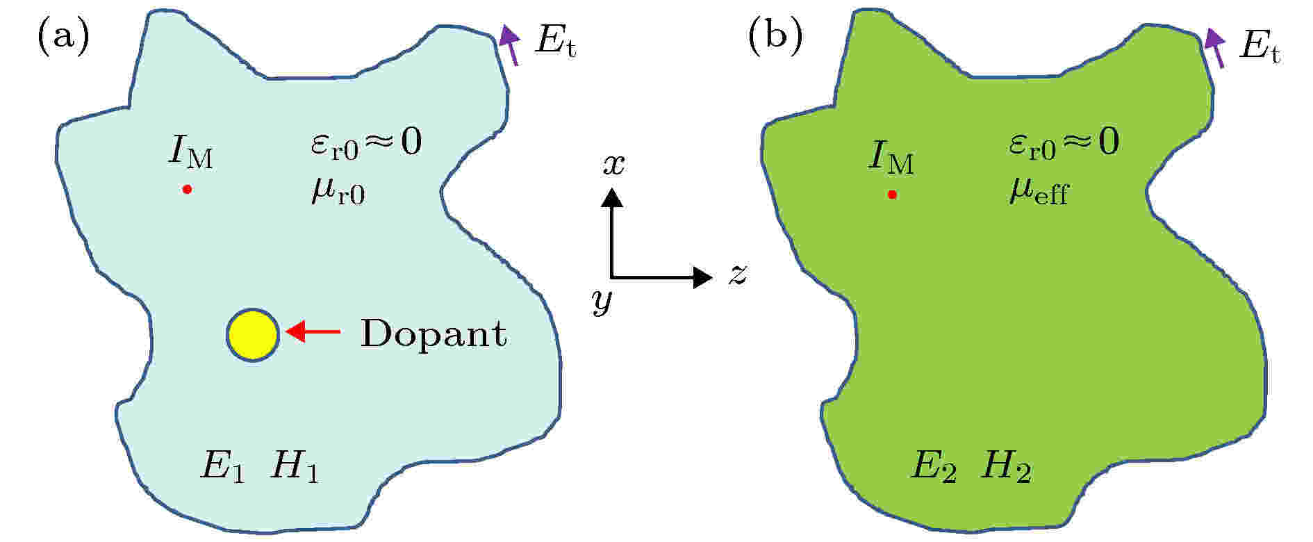
2020, 69 (15): 154201.
doi: 10.7498/aps.69.20200110
Abstract +
The perfectly matched layer plays a key role in electromagnetic simulations, and it makes the infinite space look like a finite space, so that the electromagnetic waves propagating to the boundary seem like their propagations to the infinity. The inner perfectly matched layer has a similar concept, usually in the form of a cylinder or sphere placed inside the physical field. It makes the electromagnetic field matched at the boundary, so that the electromagnetic waves propagate on its convex surface as if they were propagating to an infinite distance, without any scattering. In addition to the perfectly matched layer, planar absorbers can be realized in a variety of ways, such as spatial Kramers-Kronig relations, photonic crystals, metamaterials, etc. On the other hand, the inner cylindrical or spherical absorbers are generally perfect absorbers, electromagnetic “black hole”, etc. Transformation optics always arouse great research interests. For its property of controlling propagation of electromagnetic waves arbitrarily under coordinate mappings, transformation optics has a wide range of applications and has also been used as a theoretical tool for designing absorbers. However, to the authors’ knowledge, there is no effective method to achieve perfect absorption of inner absorbers with no reflections and independence of incident angle or wave frequency. In this paper, transformation optics theory is used to design an inner perfectly matched layer whose material parameters are obtained by a radial coordinate transformation of the complex plane. Through investigating the electromagnetic wave patterns and the two-dimensional far-field diagrams, we intuitively compare and analyse one by one the absorption characteristics of the matched and mismatched perfect absorber, electromagnetic “black hole” and the inner perfectly matched layer. It is found that the matched perfect absorber has better absorption property than mismatched one and electromagnetic “black hole”. In the electromagnetic “black hole” there appear a lot of scatterings. While our inner perfectly matched layer demonstrates the best effectiveness of absorption with no back scattering. It can be used as an absorbing kernel in electromagnetic simulations and relevant experiments.
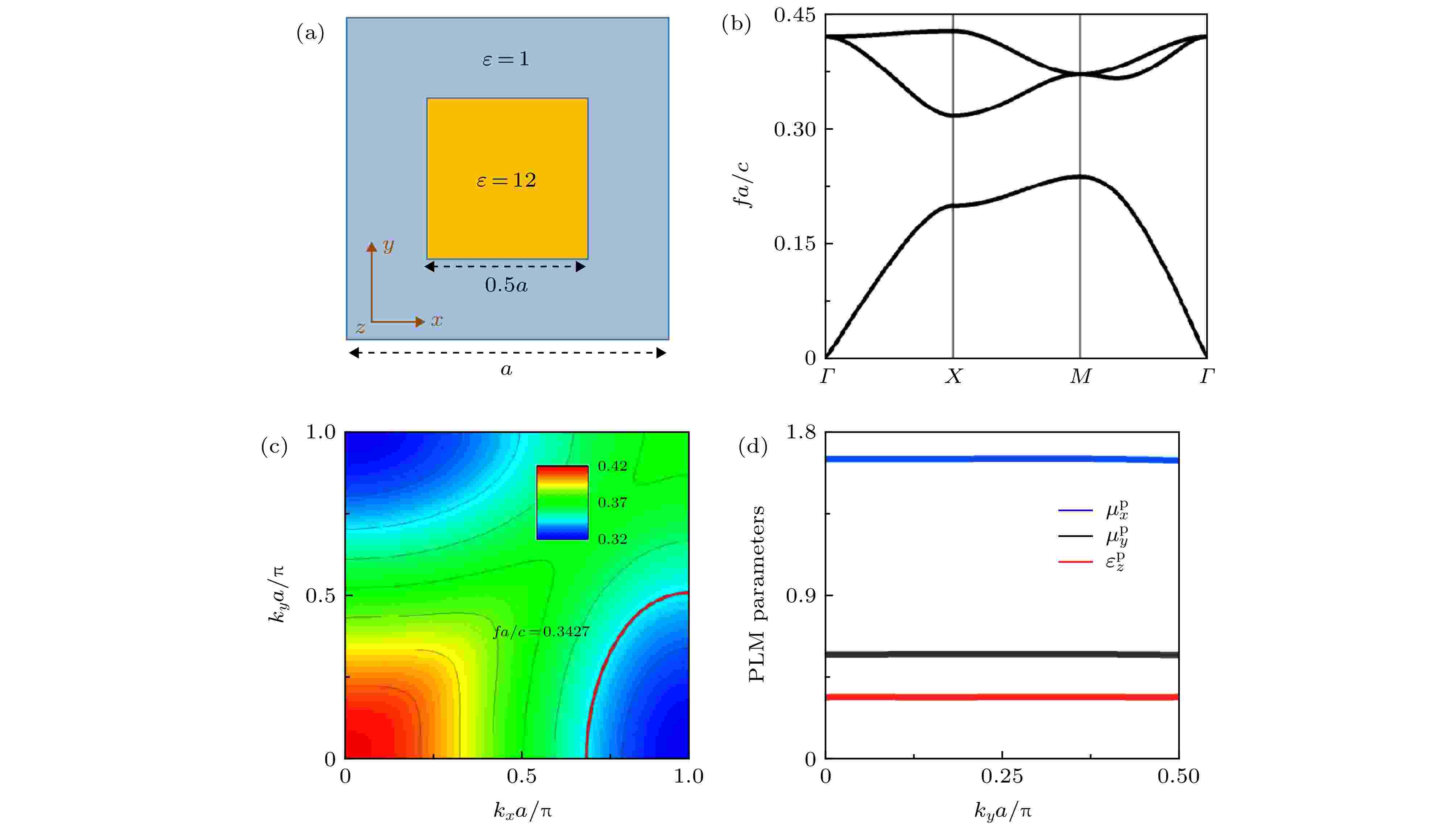
2020, 69 (15): 154203.
doi: 10.7498/aps.69.20200196
Abstract +
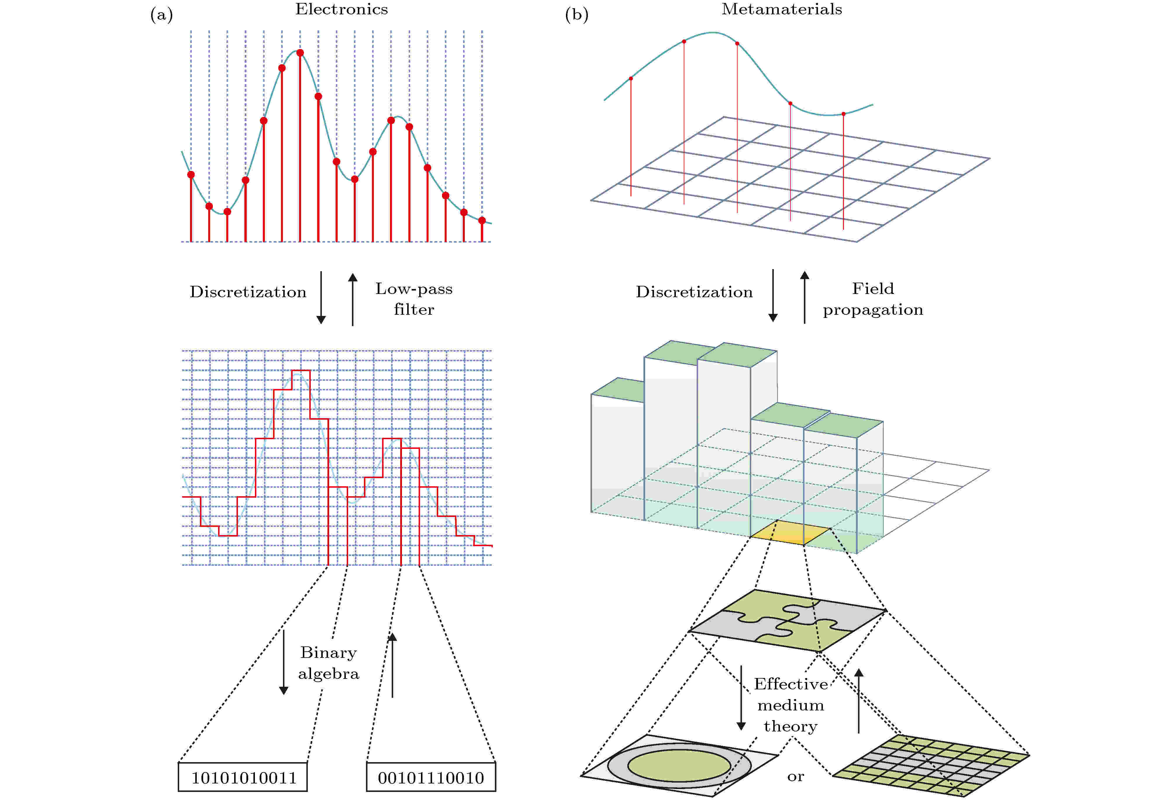
Effective medium theory is of great importance for using the artificial microstructure materials to extend the optical parameters. In this article, we develop a new kind of effective medium theory for artificial microstructures with nonlocal effects, like photonic crystals, which we name the pseudo-local effective medium theory. The optical properties of the pseudo-local effective medium are described by effective local permittivity ${\overleftrightarrow \varepsilon ^{\rm{p}}}\left( \omega \right)$ and permeability ${\overleftrightarrow \mu ^{\rm{p}}}\left( \omega \right)$ , together with an additional wave vector ${{{k}}_a}$ . We find that the pseudo-local medium exhibits a unique blend of local and nonlocal characteristics. On the surface normal to ${{{k}}_a}$ , the pseudo-local medium is optically equivalent to its local medium counterpart. While on the surface parallel to ${{{k}}_a}$ , the abnormal wave phenomena induced by inherent nonlocality, such as negative refraction and total reflection, may occur. Furthermore, it is found that a $\text{π}$ phase shift is added to transmission wave through the pseudo-local medium composed of odd number of unit cells under all incident angles. Based on this unique feature, an all-angle phase grating is proposed. Our work opens a route towards the advanced optical devices based on the pseudo-local effective media.


2020, 69 (15): 154204.
doi: 10.7498/aps.69.20200195
Abstract +
Weyl semimetal has the massless and chiral low-energy electronic excitation charateristic, and its quasi-particle behavior can be described by Weyl equation, and may lead to appealing transport properties, such as Fermi arc surface state, negative magnetic resistance, chiral Landau level, etc. By analogous with Weyl semimetal, one has realized Weyl point degeneracy of electromagnetic wave in an ideal Weyl metamaterial. In this article, by breaking the mirror symmetry of the saddle-shaped meta-atom structure, we theoretically investigate chirality-dependent split and shift effect of Weyl point frequencies which would otherwise be identical. The frequency shift can be tuned by the symmetry-broken intensity. Finally, we study the Fermi arc surface state connecting two Weyl points on $\left\langle {001} \right\rangle $ crystal surface.

REVIEW

EDITOR'S SUGGESTION
2020, 69 (15): 157801.
doi: 10.7498/aps.69.20200302
Abstract +
GENERAL
EDITOR'S SUGGESTION
2020, 69 (15): 150601.
doi: 10.7498/aps.69.20200706
Abstract +
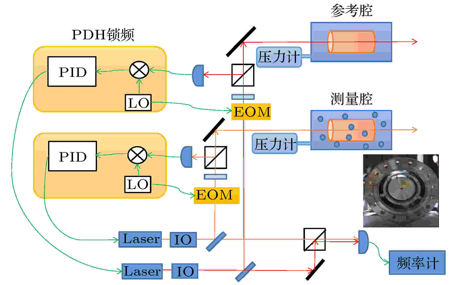
With the development of vacuum technology, subject to the influence of directional flow and uneven temperature, the thermodynamic equilibrium state is destroyed. In this case, the pressure reference is not suitable for characterizing the vacuum state. To ensure the long-term stability and reproducibility of the measurement system, vacuum metrology will be characterized by gas density. The precisive measurement of gas refractive index based on a Fabry-Perot cavity can be used to derive the gas density. This kind of an optical measurement of vacuum links macroscopic dielectric constants of gases with microscopic polarization parameters of atoms and molecules. It replaces the physical standard based on the mercury pressure gauge with the quantum standard. In this paper, we discuss the reverse process from refractive index to gas pressure, and use the laser-locked Fabry-Perot cavity method to measure the refractive index of argon gas. The contribution of related parameters to the uncertainty of determined gas pressure is analyzed. The influences of material parameters and experimental parameters such as gas molar susceptibility, molar susceptibility, dielectric second Virial coefficient and temperature on gas pressure accuracy are analyzed. The result shows that the uncertainty in our measurement of argon within 1 atm is $u = \sqrt {{{(6\;{\rm{mPa}})}^2} + {{(73 \times {{10}^{ - 6}}p)}^2}} $ . Currently, the uncertainty mainly comes from the measurement deviation of gas temperature inside the cavity. After repeating the measurement a few times, the results show that the statistical uncertainty of refractive index is within 100 ppm, which is limited by the accuracy of the pressure gauge used here. In addition, we compare the dipole calculated by the ab initio method with that by the DOSD method. The results show that the dynamic polarizability obtained by the ab initio method is consistent with our experimental results. In conclusion, these experimental results show that the measurement of gas pressure based on the gas refractive index has high repeatability and accuracy. If the temperature control and corresponding measurement accuracy of the gas are further improved, this method can also be used to obtain high-precision microscopic parameters such as the polarizabilities of atoms and molecules. In the future work, we will focus on improving the temperature control and the design of the cavity to reduce cavity leakage and deflation. It is possible that the measurement accuracy of the gas pressure will be increased to 10 ppm level, which is the same level as the current standard pressure gauge and will become a new standard for pressure measurement in the future.


2020, 69 (15): 150701.
doi: 10.7498/aps.69.20200576
Abstract +
Instrument background is an important content in implementing the space-based astronomical mission. For the focusing X-ray telescope, the observation ability is affected by the particle background, which is directly related to the sensitivity of the instrument and the systematic error of background reproducibility. In the iterative process of instrument design and engineering implementation, it is necessary to make sure that the particle background level is within the acceptable level. In this paper, we propose a method of fast estimating the particle background of the space-based focusing X-ray telescope, which is based on interpolation of planar density distribution. With acceptable accuracy and efficiency, this method is suitable for rapidly estimating the background shielding effects of various design schemes, especially in the early stage of telescope scheme design. This can greatly improve the availability of early scheme design. This method has a certain reference significance for developing the focusing space high-energy astronomical instruments and other similar instruments. The commonly used method of estimating the particle background of space X-ray instruments is the Monte Carlo method, which relies on constructing an overall mass model of instrument and simulating the response of the detectors to the space radiation environment, but the calculation efficiency of this method is lower. In order to meet the needs of instrument design optimization of mission during initial stage, we simulate the responses of simplified aluminum spherical shells with different sizes and planar desities to the space radiation environment, and count energy depositing events in a concerned energy range. Then we obtain the relationship between the particle background caused by various spatial radiation components and the thickness of the simplified aluminum spherical shell after being normalized. The particle track tracking method is used to calculate the area density distribution of the equivalent aluminum around the sensitive detectors of the telescope. Finally, the average particle background level of each component is obtained by interpolating calculation according to the relationship between equivalent thickness and the particle background. The method is verified through the simulation of the payload SFA onboard eXTP satellite by comparing the results of the simulation calculation of the whole star mass model with the results from the area density distribution interpolation method, and good consistency is obtained. The method based on the interpolation of the planar density distribution can well depict the relationship between the whole structure and the particle background level, which can be applied to the particle background estimation and shielding optimization for X-ray focusing instruments in different orbital space radiation environments.
ATOMIC AND MOLECULAR PHYSICS

Theoretical study on electronic structure and transition properties of excited states for SeH+ anion
2020, 69 (15): 153101.
doi: 10.7498/aps.69.20200278
Abstract +

PHYSICS OF GASES, PLASMAS, AND ELECTRIC DISCHARGES

2020, 69 (15): 155201.
doi: 10.7498/aps.69.20200216
Abstract +
Pulsed arc plasma excitation is characterized by strong local heating effect and wide disturbance range, and it has a broad application prospect in supersonic flow control. In this paper, by using electrical parameter measurement system and high speed schlieren technique, we study the electrical and flow field characteristics of pulsed arc plasma excitation under the condition of Ma = 3 incoming flow. The nano-particle planar laser scattering (NPLS) is used to investigate the flow structure of the supersonic flat boundary layer, and the transition characteristics of the boundary layer at different plasma excitation frequencies are studied. The experimental results show that in the flow field with Ma = 3 and the total incoming pressure P0 = 1 atm (1 atm = 1.01 × 10⁵ Pa), the peak voltage of the pulsed arc plasma actuator discharge is 6 kV, the peak current is 70 A, the time scale of the discharge is about 300 ns, the single discharge energy is 70 mJ; the pulsed arc discharge will produce the precursor shock wave with higher velocity and the thermal deposition zone with higher temperature, which will exert continuously disturbance on the boundary layer. The pulsed arc plasma excitation with perturbation can promote the transition of supersonic plate boundary layer. Moreover, the high-frequency impact effect of pulsed discharge can promote the transition to occur ahead of time, and the higher the frequency, the better the effect is. As the excitation frequency increases, the transition position of the boundary layer of the supersonic flat plate moves forward, and the length of the transition area of the boundary layer becomes shorter as the excitation frequency increases. When the excitation frequency is 60 kHz, the length of transition zone is 0 and the thickness of turbulent boundary layer is 25 mm. When a high frequency is applied (f = 40, 60 kHz), the transition path of the boundary layer is that the shock wave generated by the plasma excitation triggers the unstable wave, and the development of unstable waves directly skips the linear growth stage, passes through the bypass and transitions into turbulent flow. The pulsed arc plasma excitation can be used to promote supersonic boundary layer transition.
CONDENSED MATTER: STRUCTURAL, MECHANICAL, AND THERMAL PROPERTIES

EDITOR'S SUGGESTION
2020, 69 (15): 156201.
doi: 10.7498/aps.69.20200542
Abstract +


2020, 69 (15): 156202.
doi: 10.7498/aps.69.20200289
Abstract +
MgF2 is an important member of alkaline-earth fluorides and has a wide range of applications in industry. Meanwhile, MgF2 occurs naturally as a mineral sellaite. Compared with the study of its electronic structure and optical properties, the researches of the behavior under high pressure of MgF2, especially the thermodynamic properties are still limited. The high-pressure melting, volume thermal expansion coefficient, and thermoelastic parameter of the Earth’s lower mantle mineral, like MgF2, are of interest and importance for understanding the physical nature of the functional material and for recognizing the structural compositions, dynamics, evolution and origin of the earth. Using the first-principles calculations based on density functional theory, the thermodynamic, mechanical, and dynamic stability of the fluorite-type structure for MgF2 are systematically studied. The calculations indicate that the fluorite-type structure is a high-pressure phase and it is stable at least up to 135 GPa. According to the principle of equal enthalpies, the phase transition pressure of MgF2 crystal from stable rutile structure to high pressure fluorite structure is determined to be 19.26 GPa and 18.15 GPa based on the the generalized gradient approximation and local density approximation calculations, respectively. The high-temperature structural stability of MgF2 with the fluorite-type structure is investigated and confirmed by using the classical molecular dynamics (MD) simulations by taking into account the molar volume and total energy change behavior in a temperature range from 300 to 6000 K. On the basis of previous research, the volume thermal expansion coefficient, isothermal bulk modulus, and thermoelastic parameter of MgF2 with the CaF2-type fluorite structure are predicted systematically in a temperature range from 300 to 1500 K and in a pressure range from 0 to 135 GPa with the help of the generalized gradient approximation of the revised Perdew-Burke-Ernzerhof form combined with quasiharmonic Debye model calculations and the molecular dynamics method combined with reliable interatomic potentials. An important discovery is that the thermoelastic parameter of this material under low temperature and low pressure is not a constant as assumed usually in previous studies of the equation of states, but it approaches to a constant under both high temperature and high pressure.
CONDENSED MATTER: ELECTRONIC STRUCTURE, ELECTRICAL, MAGNETIC, AND OPTICAL PROPERTIES

2020, 69 (15): 157302.
doi: 10.7498/aps.69.20191987
Abstract +
The contacts between semiconductor and metal are vital in the fabrication of nano electronic and optoelectronic devices. The contact type has a great influence on the function realization and performance of the device. In order to prepare multifunctional devices with high performance, it is necessary to modulate the barrier height and contact type at the interface. First-principles calculations based on the density functional theory (DFT) are implemented in the VASP package. The generalized gradient approximation of Perdew, Burke, and Ernzerhof (GGA-PBE) with van der Waals (vdW) correction proposed by Grimme (DFT-D3) is chosen due to its good description of long-range vdW interactions. It is demonstrated that weak vdW interactions dominate between graphene and InSe with their intrinsic electronic properties preserved. We find that the n-type ohmic contact is formed at the graphene/InSe interface with the Fermi level through the conduction band of InSe (ΦBn < 0). The Fermi level of graphene/InSe heterostructure moves down to below the Dirac point of graphene layer, which results in p-type (hole) doping in graphene. Moreover, the external electric field is effective to tune the Schottky barrier, which can control not only the Schottky barrier height but also the type of contact. With the negative external electric field varying from 0 to –1 V/nm, the conduction band minimum of InSe below the Fermi level declines gradually but the n-type ohmic contact is still preserved. Nevertheless, with the positive external electric field varying from 0 to 0.8 V/nm, the conduction band minimum of InSe shifts upward and across the Fermi level, the conduction band minimum of InSe is closer to the Fermi level than the valence band maximum, which indicates that the n-type Schottky contact is formed. The Fermi level moves from the the conduction band minimum to the valence band maximum of InSe when the positive external electric field increases from 0.8 V/nm to 2 V/nm. The n-type Schottky barrier height exceeds the p-type Schottky barrier height gradually, which demonstrates that the positive external electric field transforms the n-type Schottky contact into the p-type Schottky contact at the graphene/InSe interface. When the positive external electric field exceeds 2 V/nm, the valence band of InSe moves upward and cross the Fermi level (ΦBp < 0), the ohmic contact is obtained again. Meanwhile, p-type (hole) doping in graphene is enhanced under negative external electric field and a large positive external electric field is required to achieve n-type (electron) doping in graphene. The external electric field can control not only the amount of charge transfer but also the direction of charge transfer at the graphene/InSe interface.
2020, 69 (15): 157303.
doi: 10.7498/aps.69.20200250
Abstract +

INTERDISCIPLINARY PHYSICS AND RELATED AREAS OF SCIENCE AND TECHNOLOGY
2020, 69 (15): 158102.
doi: 10.7498/aps.69.20200261
Abstract +
All-inorganic cesium lead halide (CsPbX3, X = Cl, Br, I) perovskite nanocrystals (NCs) are promising candidates for the next-generation luminescent materials due to their fascinating physic-optical properties, such as size-tunable optical band gaps, high luminescent quantum yields, and narrow emissive bandwidths. At present, the prepared CsPbX3 NCs are concentrated in the range of green and red. The research of blue CsPbX3 NCs is lacking and these CsPbX3 NCs still suffer problems of low quantum efficiency and poor stability, which limit their application areas. In this paper, 2-acrylamide-2-methyl-propionic sulfonic acid (AMPS) with strong electronegativity is used to prepare CsPbX3 NCs by the thermal injection method. All CsPbBr3 NCs each have a uniform size, good crystallization, and nanoplate morphology. The CsPbBr3 NCs each exhibit an optical absorption at 450 nm and a photoluminescence (PL) emission at 462 nm with a full width of half maximum of 20 nm. To further investigate the physical mechanism of the PL shift and explore the effect of AMPS on the transient dynamics of the photocarriers in CsPbBr3 NCs, we measure the time-resolved PL spectrum and transient absorption spectrum. It can be found that the CsPbBr3 NCs have only one lifetime of 222 ns, which is one order of magnitude longer than that of the CsPbBr3 NCs without AMPS. Meanwhile, there is no obvious transient absorption signal. Based on the above experimental results, this blue shift is caused by three reasons. Firstly, AMPS has a strong attraction to the excited electrons, which causes the electrons in the excited state to stay for a long time before returning to the ground state. Because of the relaxation behavior before the radiation transition, the energy released by the radiation transition is larger and the fluorescence wavelength is shorter. Secondly, the prepared CsPbBr3 NCs have stronger quantum confinement than CsPbBr3 NCs with cubic block morphology. Finally, AMPS can passivate the surface defects of CsPbBr3 NCs more effectively. The prepared CsPbBr3 NCs have less defects, which also causes the PL to be blue-shifted. This study provides not only a method of synthsizing the CsPbBr3 NCs with blue emitting but also an insight into the surface engineering or physical functionalization of inorganic perovskite NCs.
2020, 69 (15): 158401.
doi: 10.7498/aps.69.20200314
Abstract +
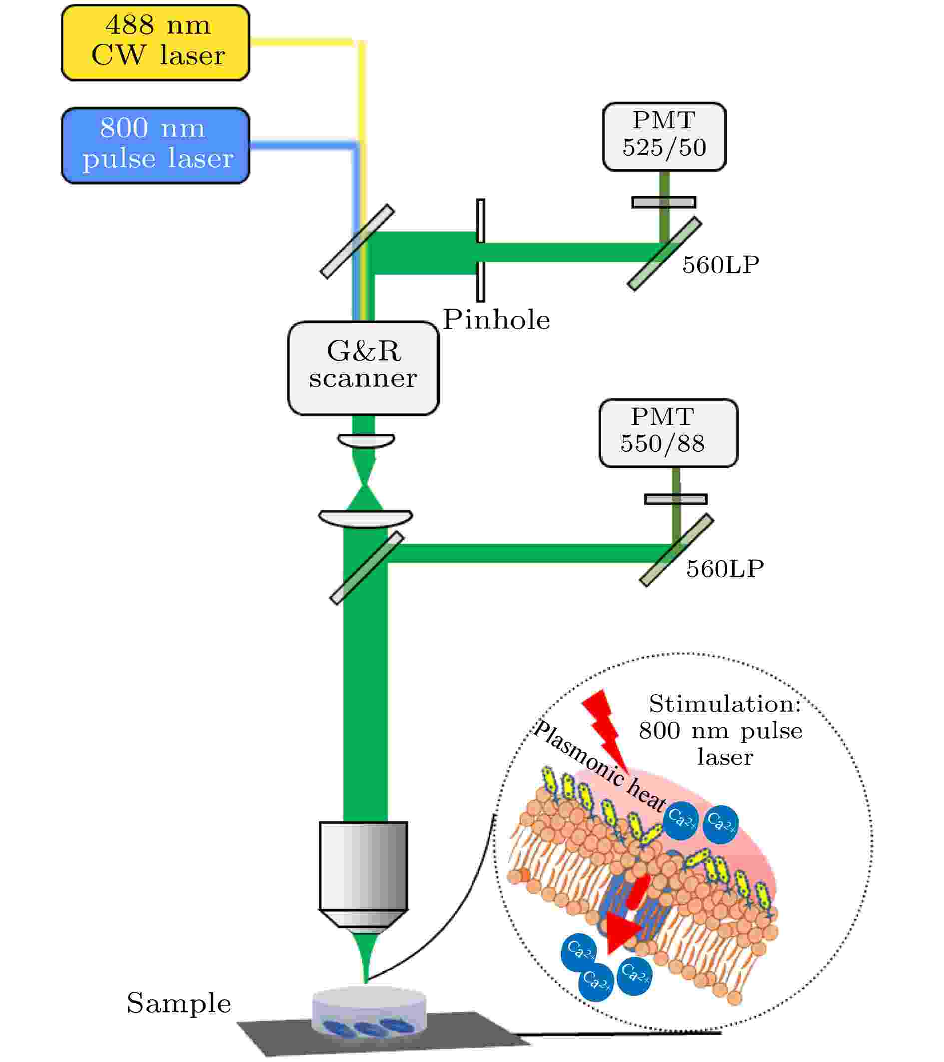
2020, 69 (15): 158701.
doi: 10.7498/aps.69.20200489
Abstract +
Calcium ions (Ca2+) play a key role of the nerve cells generating universal intracellular signals and controlling important functions. Ca2+ activation is of great significance for explaining the subcellular-level biological process. Light stimulated nerve cells to control intracellular signals and membrane activities has become a main method in neuroscience, and the photoactivation is one of the main ways to study intracellular Ca2+ transmission. Nerve cells can be directly stimulated by light to produce action potentials, but such techniques are inaccurate in the delivered light energy. To improve this, here in this work we show that gold nanorods (GNRs) can be conjugated to ligands to bound to human neuroblast cells (SH-SY5Y), and introduce an optical method of stimulating and monitoring Ca2+ signal in nerve cells in which the plasmonic excitation of GNRs is used. In this paper, we use confocal microscopy to display the 488 nm continuous wave laser irradiating SH-SY5Y cells with Ca2+ indicator (Fluo-4, AM) to check fluorescence. Near-infrared pulsed light at the plasmon resonance absorption peak of GNRs is used to stimulate Ca2+ signal transduction in SH-SY5Y labeled with GNRs, and Fluo-4, AM is used for two-photon excited fluorescence imaging. In addition, we use the pulsed laser with power of 0.5 mW and a wavelength of 800 nm. The Ca2+ activation can be achieved in 10 s on average. The release rate of Ca2+ from SH-SY5Y cells labeled with GNRs is 6 times that without GNRs. Next, in order to determine the source of changes in Ca2+, we use the BPATA to deplete the intracellular Ca2+, after 5 min, 200 μmol/L Ca2+ solution is added, and its ΔF/F is found to be more than 1.5 times that without GNRs. Thus, we believe that GNRs could enhance photoactivation through local surface plasmon resonance induced membrane depolarization and generate an action potential. The results prove the feasibility of using GNRs to enhance the activation of Ca2+ in nerve cells, and provide an optical means of lower photodamage and more precise for studying nerve cell ion channels. Our study demonstrates that enhancing photoactivation by GNRs could provide an outlook of basic research in neuroscience.
