


-
Transition-metal dichalcogenides with exceptional electrical and optical properties have emerged as a new platform for atomic-scale optoelectronic devices. However, the poor optical absorption resists their potential applications. In this paper, monolayer molybdenum disulfide four-band perfect absorber based on critical coupling and guided mode resonance is proposed theoretically and numerically by the finite difference time domain method. Meanwhile, the physical mechanism can be better analyzed through impedance matching and coupled mode theory. Monolayer molybdenum disulfide is placed between the silicon dioxide and a two-dimensional polymethyl methacrylate layer with a periodic square-shaped air groove structure. The three form a sandwich-like stacked structure similar to a rectangle. The bottom of the absorber uses a silver layer as the back reflection layer. Using the critical coupling principle of guided resonance, the high-efficiency light absorption of the monolayer molybdenum disulfide is obtained, that is, four perfect resonances are obtained at the resonance wavelengths (λ1 = 510.0 nm, λ2 = 518.8 nm, λ3 = 565.9 nm, and λ4 = 600.3 nm), the absorption rates are 99.03%, 98.10%, 97.30%, and 95.41%, and the average absorption rate is as high as 97.46% in the visible light spectrum range, which is over 12 times more than that of a bare monolayer MoS2. The simulation results show that the adjusting of the geometric parameters of the structure can control the range of the resonance wavelength of the monolayer molybdenum disulfide, the system experiences three states, i.e. under-coupling, critical coupling, and over-coupling because of the leakage rate of resonance, thereby exhibiting advantageous tunability of operating wavelength in monolayer MoS2, which has important practical significance for improving the absorption intensity and selectivity of the monolayer molybdenum disulfide. The novel idea of using critical coupling to enhance the light-MoS2 interaction can also be adopted in other atomically thin materials. At the same time, in this article the sensing performance of the absorber is discussed, and it is found that the highest quality factor, sensitivity and figure of merit of the sensor are 1294.1, 155.1 nm/RIU, and 436, respectively. The proposed structure is simple and the program is versatile. And these results indicate that the designed structure may offer a promising technology for improving the light-matter interaction in two-dimensional transition metal binary compounds, and has excellent application prospects in wavelength selective photoluminescence and photodetection. -
Keywords:
- critical coupling /
- molybdenum disulfide /
- perfect absorption /
- visible light spectrum range
[1] Smith D R, Padilla W J, Vier D C, Nemat-Nasser S C, Schultz S 2000 Phys. Rev. Lett. 84 4184
 Google Scholar
[2] Smith D R, Vier D C, Koschny T, Soukoulis C M 2005 Phys. Rev. E. 71 036617
Google Scholar
[3] Smith D R, Pendry J B, Wiltshire M C K 2004 Science 305 788
Google Scholar
[4] Pendry J B 2000 Phys. Rev. Lett. 85 3966
Google Scholar
[5] Pendry J B, Schurig D, Smith D R 2006 Science 312 1780
Google Scholar
[6] Cai W, Chettiar U K, Kildishev A V, Shalaev V M 2007 Nat. Photonics 1 224
Google Scholar
[7] Landy N I, Sajuyigbe S, Mock J J, Smith D R, Padilla W J 2008 Phys. Rev. Lett. 100 207402
Google Scholar
[8] Wang X X, Zhu J K, Xu Y Q, Qi Y P, Zhang L P, Yang H, Yi Z 2021 Chin. Phys. B 30 024207
Google Scholar
[9] Lee K, Choi H J, Son J, Park H S, Ahn J, Min B 2015 Sci. Rep. 5 14403
Google Scholar
[10] Liu Z M, Zhang X, Zhang Z B, Gao E D, Zhou F Q, Li H J, Luo X 2020 New J. Phys. 22 083006
Google Scholar
[11] Song S C, Chen Q, Jin L, Sun F H 2013 Nanoscale 5 9615
Google Scholar
[12] Yi Z, Li J K, Lin J C, Qin F, Chen X F, Yao W T, Liu Z M, Cheng S B, Wu P H, Li H L 2020 Nanoscale 12 23077
Google Scholar
[13] 徐依全, 王聪 2020 物理学报 69 184216
Google Scholar
Xu Y Q, Wang C 2020 Acta Phys. Sin. 69 184216
Google Scholar
[14] Sun Z, Chang H 2014 ACS Nano 8 4133
Google Scholar
[15] 许杰, 周丽, 黄志祥, 吴先良 2015 物理学报 64 238103
Google Scholar
Xu J, Zhou L, Huang Z X, Wu X L 2015 Acta Phys. Sin. 64 238103
Google Scholar
[16] 谢剑锋, 曹觉先 2013 物理学报 62 017302
Google Scholar
Xie J F, Cao J X 2013 Acta Phys. Sin. 62 017302
Google Scholar
[17] Mak K F, Shan J 2016 Nat. Photonics 10 216
Google Scholar
[18] Zhang Y, Shi Y, Liang C 2016 Opt. Mater. Express 6 3036
Google Scholar
[19] Li J S, Sun J Z 2019 Appl. Phys. B 125 183
Google Scholar
[20] Li J K, Chen X F, Yi Z, Yang H, Tang Y J, Yi Y, Yao W T, Wang J Q, Yi Y G 2020 Mater. Today Energy 16 100390
Google Scholar
[21] Splendiani A, Sun L, Zhang Y, Li T, Kim J, Chim C Y, Galli G, Wang F 2010 Nano Lett. 10 1271
Google Scholar
[22] Li J K, Chen Z Q, Yang H, Yi Z, Chen X F, Yao W T, Duan T, Wu P H, Li G F, Yi Y G 2020 Nanomaterials 10 257
Google Scholar
[23] Bahauddin S M, Robatjazi H, Thomann I 2016 ACS Photonics 3 853
Google Scholar
[24] Lopez-Sanchez O, Lembke D, Kayci M, Radenovic A, Kis A 2013 Nat. Nanotechnol. 8 497
Google Scholar
[25] Sobhani A, Lauchner A, Najmaei S, Ayala-Orozco C, Wen F, Lou J, Halas N J 2014 Appl. Phys. Lett. 104 031112
Google Scholar
[26] Late D J, Liu B, Matte H S, Dravid V P, Rao C N R 2012 ACS Nano 6 5635
Google Scholar
[27] Bernardi M, Palummo M, Grossman J C 2013 Nano Lett. 13 3664
Google Scholar
[28] Janisch C, Song H, Zhou C, Lin Z, Elías A L, Ji D, Liu Z 2016 2D Mater. 3 025017
Google Scholar
[29] Liu J T, Wang T B, Li X J, Liu N H 2014 J. Appl. Phys. 115 193511
Google Scholar
[30] Lu H, Gan X, Mao D, Fan Y, Yang D, Zhao J 2017 Opt. Express 25 21630
Google Scholar
[31] Cao J, Wang J, Yang G, Lu Y, Sun R, Yan P, Gao S 2017 Superlattices Microstruct. 110 26
Google Scholar
[32] Zheng J B, Barton R A, Englund D 2014 ACS Photonics 1 768
Google Scholar
[33] Piper J R, Fan S H 2016 ACS Photonics 3 3571
Google Scholar
[34] Li Y, Chernikov A, Zhang X, Rigosi A, Hill H M, Van der Zande A M, Chenet D A, Shih E M, Hone J, Heinz T F 2014 Phys. Rev. B 90 205422
Google Scholar
[35] Bade W 1957 Chem. Phys. 27 1280
Google Scholar
[36] Cheng L, Wang T, Jiang X, Yan X, Xiao S 2015 J. Phys. D 50 435104
Google Scholar
[37] Qin F, Chen X F, Yi Z, Yao W T, Yang H, Tang Y J, Yi Y, Li H L, Yi Y G 2020 Sol. Energy Mater. Sol. Cells 211 110535
Google Scholar
[38] He Z H, Li L Q, Ma H Q, Pu L H, Xu H, Yi Z, Cao X L, Cui W 2021 Results Phys. 21 103795
Google Scholar
[39] Haus H A, Huang W 1991 Proc. IEEE 79 1505
Google Scholar
[40] Li Q, Wang T, Su Y, Yan M, Qiu M 2010 Opt. Express 18 8367
Google Scholar
[41] An S, Lv J, Yi Z, Liu C, Yang L, Wang F, Liu Q, Su W, Li X, Sun T, Chu P 2021 Optik 226 165779
Google Scholar
[42] Qing Y M, Ma H F, Cui T J 2018 Opt. Express 26 32442
Google Scholar
[43] El-Aasser M A, Mahmoud S A 2017 Optoelectron. Adv. Mater. Rapid Commun. 118 398
[44] Li J Y, Wang S F, Sun G G, Gao H J, Yu X L, Tang S N, Zhao X X, Yi Z, Wang Y, Wei Y 2021 Mater. Today Chem. 19 100390
Google Scholar
[45] Wang S, Magnusson R 1993 Appl. Opt. 32 2606
Google Scholar
[46] Pan M, Su Z, Yu Z, Wu P, Jile H, Yi Z, Chen Z 2020 Result. Phys. 19 103415
Google Scholar
[47] Zhang X, Liu Z, Zhang Z, Gao E, Luo X, Zhou F, Li H, Yi Z 2020 Opt. Express 28 36771
Google Scholar
[48] Chu P X, Chen J X, Xiong Z G, Yi Z 2020 Opt. Commun. 476 126338
Google Scholar
[49] Zhang Y B, Yi Z, Wang X Y, Chu P X, Yao W T, Zhou Z G, Cheng S B, Liu Z M, Wu P H, Pan M, Yi Y G 2021 Physica E 127 114526
Google Scholar
[50] Guo C, Zhu Z, Yuan X, Ye W, Liu K, Zhang J, Xu Wei, Qin S 2016 Adv. Opt. Mater. 4 1955
Google Scholar
[51] Li H, Qin M, Wang L, Zhai X, Ren R, Hu J 2017 Opt. Express 25 31612
Google Scholar
[52] Cao J T, Yang J F, Gu Y, Fang X D, Lu N Y, Hua B, Yan.X M 2019 Mater. Res. Express. 6 15050
Google Scholar
[53] Piper J. R, Liu V, Fan S 2014 Appl. Phys. Lett. 104 251110
Google Scholar
[54] Sourav A, Li Z W, Huang Z H, Botcha V D, Hu C, YAO J P, Peng F, Kuo H C, Wu J, Liu X K, Ang K W, Transparent L S 2018 Adv. Opt. Mater. 6 1800461
Google Scholar
[55] Qi Y, Zhang B, Liu C, Deng X 2020 IEEE Access 8 116675
Google Scholar
[56] Jiang L Y, Yuan C, Li Z Y, Su J, Yi Z, Yao W T, Wu P, Liu Z M, Cheng S B, Pan M 2021 Diamond Relat. Mater. 111 108227
Google Scholar
[57] Yu P Q, Yang H, Chen X F, Yi Z, Yao W T, Chen J F, Yi Y G, Wu P H 2020 Renewable Energy 158 227
Google Scholar
[58] Deng Y H, Yang Z J, He J 2018 Opt. Express 26 31116
Google Scholar
[59] Maurer T, Nicolas R, Lévêque G, Subramanian P, Proust J, Béal J, Schuermans S, Vilcot J P, Herro Z, Kazan M, Plain J, Boukherroub R, Akjouj A, Djafari-Rouhani B, Adam P M, Szunerits S 2014 Plasmonics 9 507
Google Scholar
[60] Lu X, Zhang L, Zhang T 2015 Opt. Express 23 20715
Google Scholar
[61] Lin L H, Zheng Y B 2015 Sci. Rep. 5 14788
Google Scholar
[62] Ye J, Dorpe P V 2011 Plasmonics 6 665
Google Scholar
[63] Ameling R, Langguth L, Hentschel M, Mesch M, Braun P V, Giessen H 2010 Appl. Phys. Lett. 97 253116
Google Scholar
[64] Huang C, Ye J, Wang S, Stakenborg T, Lagae L 2012 Appl. Phys. Lett. 100 173114
Google Scholar
-
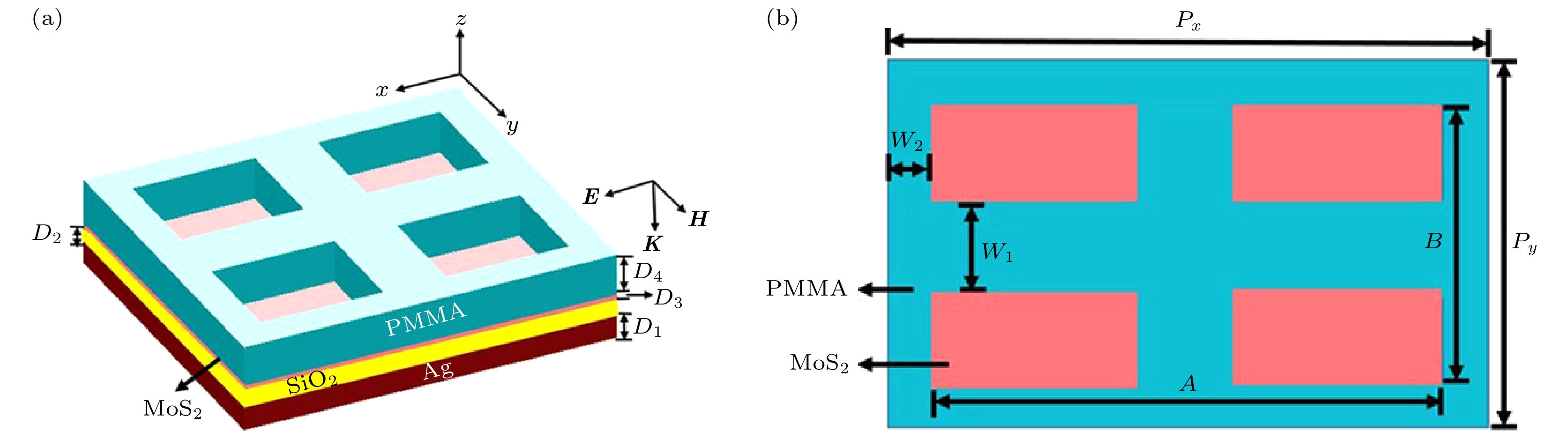
图 1 (a) 单层MoS2吸收增强系统的3D示意图; (b) 对应的俯视图; 具体的几何参数如图中所示
Figure 1. (a) 3D schematic diagram of monolayer MoS2 absorption enhancement system; (b) the corresponding top view. The specific geometric parameters are shown in the figure.
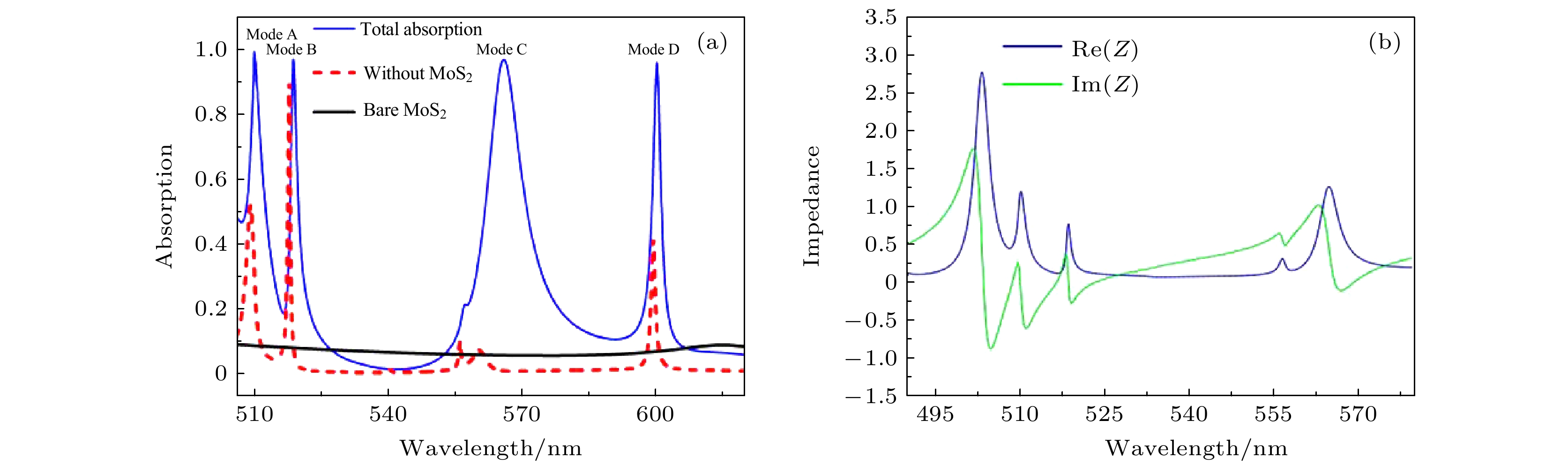
图 2 (a) 在D1 = 220 nm, D2 = 175 nm, D3 = 0.615 nm, D4 = 380 nm, Px = 1010 nm, Py = 890 nm, W1 = 89 nm, W2 = 170 nm, A = 832 nm, B = 712 nm时完美吸收器中的MoS2单层(蓝线)的吸收光谱, 为了进行比较, 示出了无MoS2整个吸收器(红线)和裸MoS2单层(黑线)的光吸收光谱(图中Mode A对应吸收峰1, Mode B对应吸收峰2, Mode C对应吸收峰3, Mode D对应吸收峰4); (b)理想吸收峰的有效阻抗的实部(蓝线Re(Z))和虚部(绿线Im(Z))
Figure 2. (a) Absorption spectrum of MoS2 monolayer (blue line) in the perfect absorber at D1 = 220 nm, D2 = 175 nm, D3 = 0.615 nm, D4 = 380 nm, Px = 1010 nm, Py = 890 nm, W1 = 89 nm, W2 = 170 nm, A = 832 nm, B = 712 nm. For comparison, the light absorption spectra of the entire absorber without MoS2 (red line) and bare MoS2 monolayer (black line) are shown (Mode A corresponds to absorption peak 1, Mode B corresponds to absorption peak 2, Mode C corresponds to absorption peak 3, Mode D corresponds to absorption peak 4); (b) the real part (blue line Re(Z)) and imaginary part (green line Im(Z)) of the effective impedance showing the ideal absorption peak.
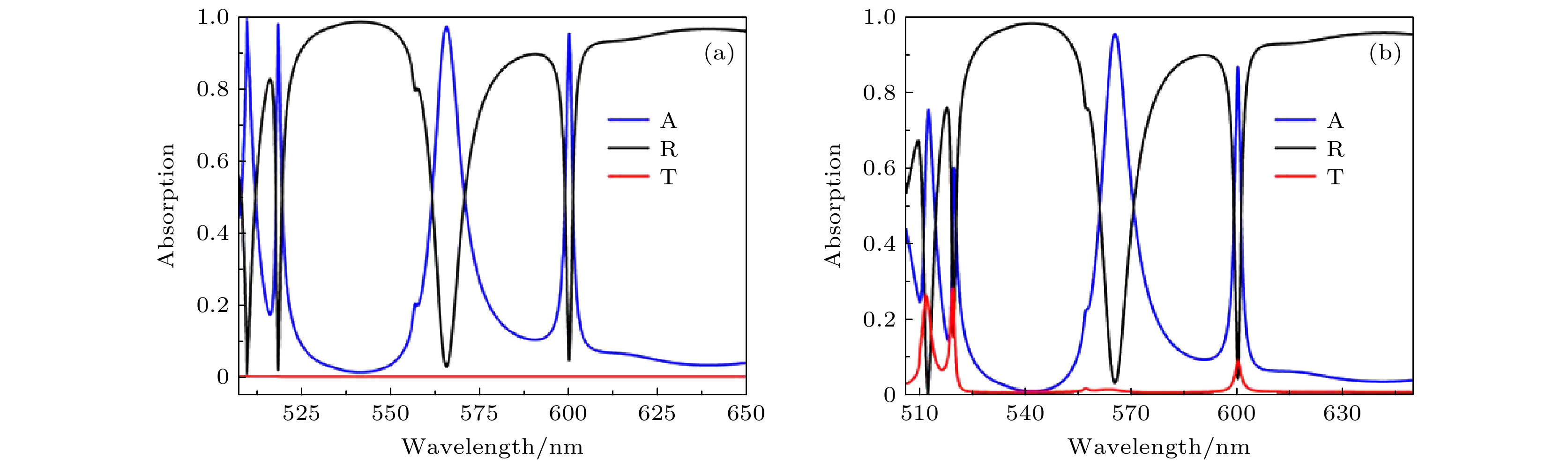
图 3 正常TM偏振光下含(a) 和不含 (b) 银反射层结构的吸收、反射和透射光谱的数值计算, 其中A代表吸收, R代表反射, T代表透射
Figure 3. Numerical calculation of the absorption, reflection and transmission spectra of the structure with (a) and without (b) silver layer under normal TM polarized light, where A represents absorption, R represents reflection, and T represents transmission.

图 4 在D1 = 220 nm, D2 = 175 nm, D3 = 0.615 nm, D4 = 380 nm, Px = 1010 nm, Py = 890 nm, A = 832 nm, B = 712 nm条件下, 空气槽为(a) 长方体、(b) 交叉椭圆盘与 (c) 三棱柱时的吸收光谱
Figure 4. Absorption spectra when the air groove is (a) cuboid, (b) cross-elliptic disk, (c) triangular prism. D1 = 220 nm, D2 = 175 nm, D3 = 0.615 nm, D4 = 380 nm, Px = 1010 nm, Py = 890 nm, A = 832 nm, B = 712 nm,
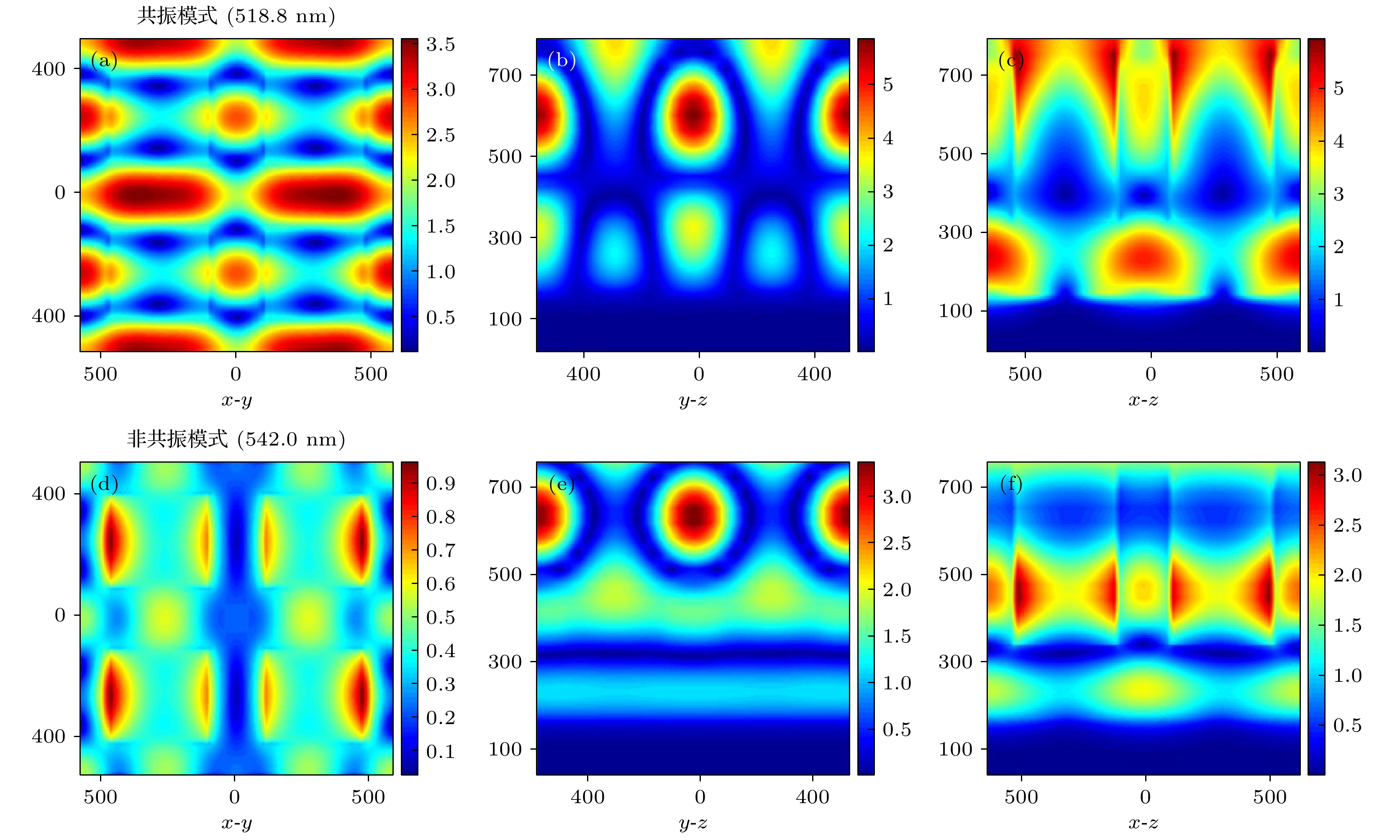
图 5 MoS2吸收器在(a)−(c) 共振模式B (共振波长为518.8 nm)下x -y, y -z和x -z截面的电场(|E|)分布的模拟结果; 在垂直入射下, (d)−(f) 非共振模式(非共振波长542.0 nm)时其x -y, y -z和x -z截面的电场(|E|)分布的模拟结果
Figure 5. Simulated electric field (|E|) distributions of (a)−(c) resonance mode B (resonant wavelength of 518.8 nm) in x -y, y -z and x -z based on the MoS2 absorber; (d)−(f) simulated electric field (|E|) distributions of non-resonant mode (non-resonant wavelength 542.0 nm) in x -y, y -z and x -z under normal incidence.

图 6 (a)−(d) x -y截面的电场图; (e)−(h) y -z截面的电场图; (i)−(l) x -z截面的电场图 (图中Mode A对应吸收峰1, Mode B对应吸收峰2, Mode C对应吸收峰3, Mode D对应吸收峰4, λ1 = 510.0 nm, λ2 = 518.8 nm, λ3 = 565.9 nm, λ4 = 600.3 nm)
Figure 6. (a)−(d) Electric field diagrams of the x -y cross section; (e)−(h) the electric field diagrams of the y -z cross section; (i)−(l) the electric field diagrams of the x -z cross section. Mode A corresponds to absorption peak 1, Mode B corresponds to absorption peak 2, Mode C corresponds to absorption peak 3, Mode D corresponds to absorption peak 4. λ1 = 510.0 nm, λ2 = 518.8 nm, λ3 = 565.9 nm, λ4 = 600.3 nm.
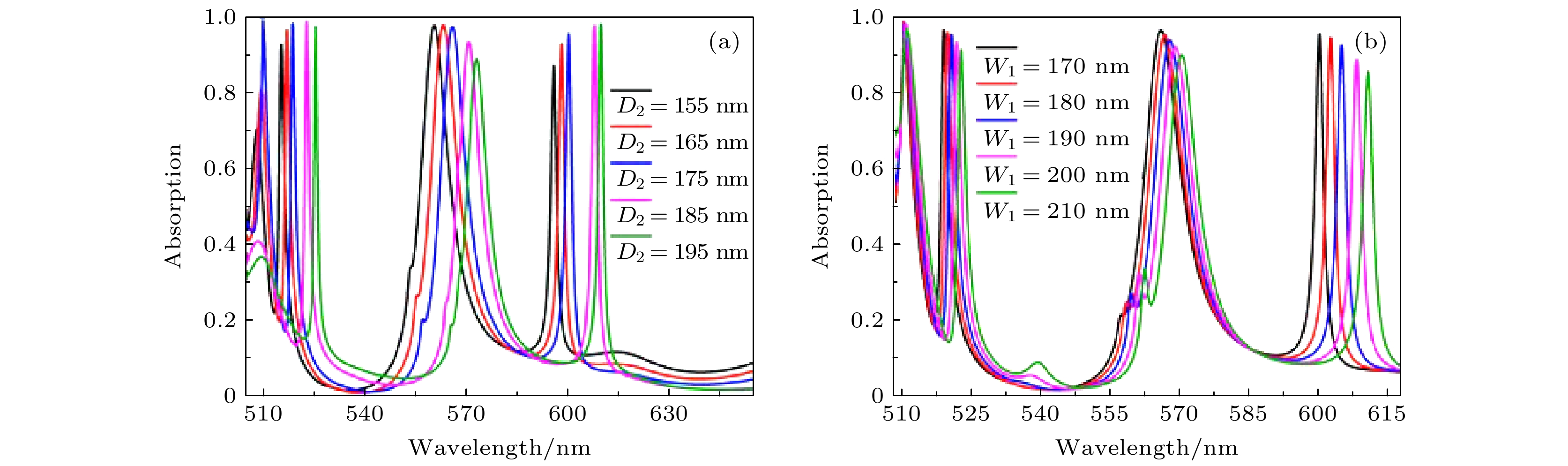
图 7 (a) 当D2从155 nm增长到195 nm时, 结构对应的光吸收情况; (b) 当W1从170 nm增长到210 nm时, 结构对应的光吸收情况
Figure 7. (a) Corresponding light absorption of the structure when D2 increases from 155 to 195 nm; (b) the corresponding light absorption of the structure when W1 increases from 170 to 210 nm.
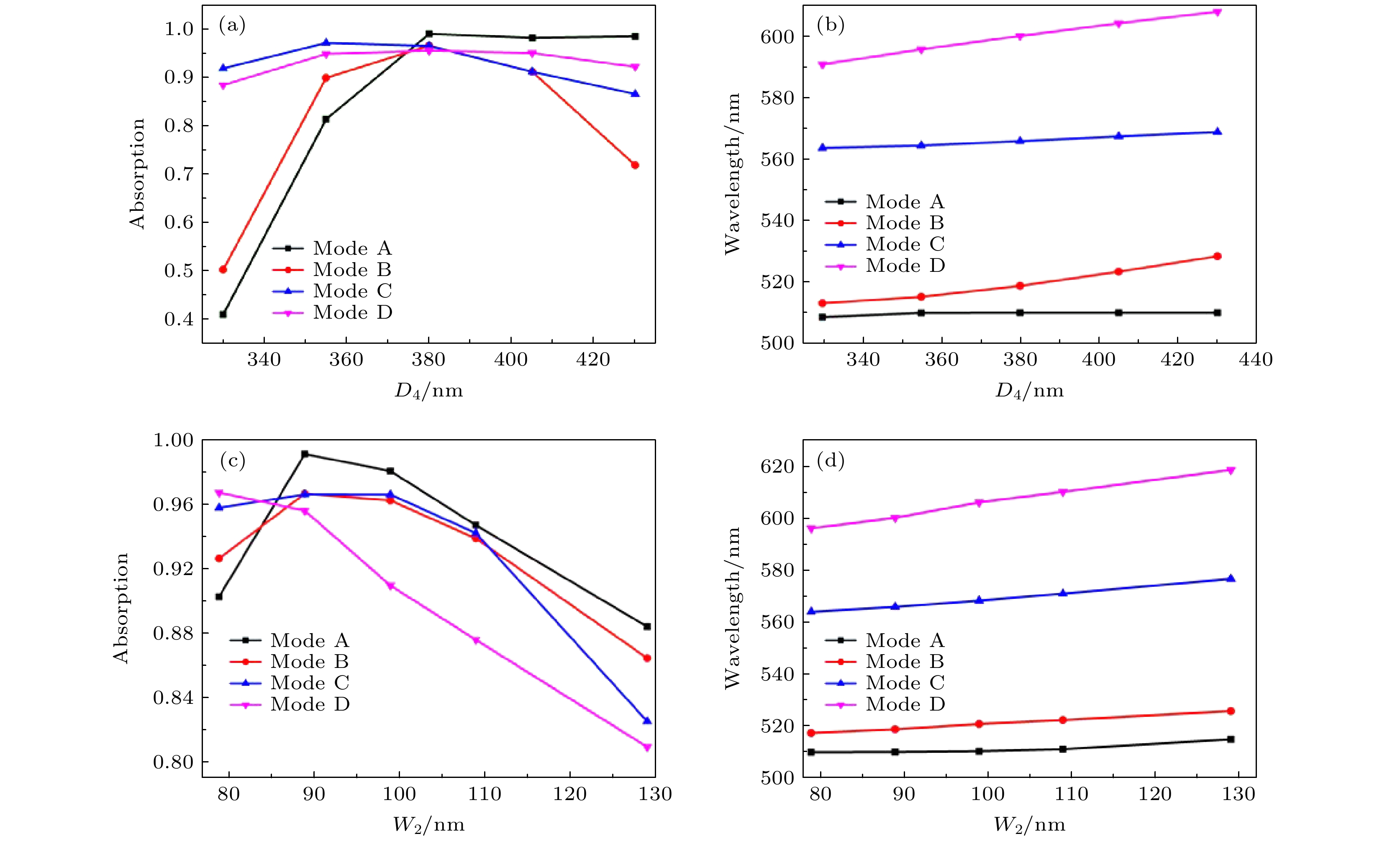
图 8 (a) D4与吸收率的关系图; (b) D4与对应共振波长范围的关系图; (c) W2与吸收率的关系图; (d) W2与对应共振波长范围的关系图; 图中Mode A对应吸收峰1, Mode B对应吸收峰2, Mode C对应吸收峰3, Mode D对应吸收峰4
Figure 8. (a) Relationship diagram between D4 and the absorption rate; (b) the relationship diagram between D4 and the corresponding resonance wavelength range; (c) the relationship diagram between W2 and the absorption rate; (d) the relationship diagram between W2 and the corresponding resonance wavelength range. Mode A corresponds to absorption peak 1, Mode B corresponds to absorption peak 2, Mode C corresponds to absorption peak 3, Mode D corresponds to absorption peak 4.

图 9 (a)−(d) 保持其他参数不变, 周期与吸收峰波长和品质因子的函数关系(图中Mode A对应吸收峰1, Mode B对应吸收峰2, Mode C对应吸收峰3, Mode D对应吸收峰4)
Figure 9. (a)−(d) Relationship among the period, the absorption peak wavelength, and Q-factor (quality factor) when other parameters are kept constant (Mode A corresponds to absorption peak 1, Mode B corresponds to absorption peak 2, Mode C corresponds to absorption peak 3, Mode D corresponds to absorption peak 4).

图 10 (a) 四个共振峰的吸收光谱随周围介质折射率的变化而移动; (b)−(e)当周围传感介质的折射率发生变化时(折射率从1.0到1.08, 间隔为0.02), 四个峰值的FOM与FWHM和波长的关系图 (图中Mode A对应吸收峰1, Mode B对应吸收峰2, Mode C对应吸收峰3, Mode D对应吸收峰4)
Figure 10. (a) Absorption spectra of the four resonance peaks move with the change in the refractive index of the surrounding medium; (b)−(e) when the refractive index of the surrounding sensing medium changes (the refractive index is from 1.0 to 1.08, the interval is 0.02), the relationships of FOM value of the four peaks and FWHM to wavelength (Mode A corresponds to absorption peak 1, Mode B corresponds to absorption peak 2, Mode C corresponds to absorption peak 3, Mode D corresponds to absorption peak 4).
表 1 所提出的吸收器与其他类似吸收器的比较
Table 1. Comparisons of the proposed absorber with other similar absorbers.
 DownLoad: CSV
-
[1] Smith D R, Padilla W J, Vier D C, Nemat-Nasser S C, Schultz S 2000 Phys. Rev. Lett. 84 4184
Google Scholar
[2] Smith D R, Vier D C, Koschny T, Soukoulis C M 2005 Phys. Rev. E. 71 036617
Google Scholar
[3] Smith D R, Pendry J B, Wiltshire M C K 2004 Science 305 788
Google Scholar
[4] Pendry J B 2000 Phys. Rev. Lett. 85 3966
Google Scholar
[5] Pendry J B, Schurig D, Smith D R 2006 Science 312 1780
Google Scholar
[6] Cai W, Chettiar U K, Kildishev A V, Shalaev V M 2007 Nat. Photonics 1 224
Google Scholar
[7] Landy N I, Sajuyigbe S, Mock J J, Smith D R, Padilla W J 2008 Phys. Rev. Lett. 100 207402
Google Scholar
[8] Wang X X, Zhu J K, Xu Y Q, Qi Y P, Zhang L P, Yang H, Yi Z 2021 Chin. Phys. B 30 024207
Google Scholar
[9] Lee K, Choi H J, Son J, Park H S, Ahn J, Min B 2015 Sci. Rep. 5 14403
Google Scholar
[10] Liu Z M, Zhang X, Zhang Z B, Gao E D, Zhou F Q, Li H J, Luo X 2020 New J. Phys. 22 083006
Google Scholar
[11] Song S C, Chen Q, Jin L, Sun F H 2013 Nanoscale 5 9615
Google Scholar
[12] Yi Z, Li J K, Lin J C, Qin F, Chen X F, Yao W T, Liu Z M, Cheng S B, Wu P H, Li H L 2020 Nanoscale 12 23077
Google Scholar
[13] 徐依全, 王聪 2020 物理学报 69 184216
Google Scholar
Xu Y Q, Wang C 2020 Acta Phys. Sin. 69 184216
Google Scholar
[14] Sun Z, Chang H 2014 ACS Nano 8 4133
Google Scholar
[15] 许杰, 周丽, 黄志祥, 吴先良 2015 物理学报 64 238103
Google Scholar
Xu J, Zhou L, Huang Z X, Wu X L 2015 Acta Phys. Sin. 64 238103
Google Scholar
[16] 谢剑锋, 曹觉先 2013 物理学报 62 017302
Google Scholar
Xie J F, Cao J X 2013 Acta Phys. Sin. 62 017302
Google Scholar
[17] Mak K F, Shan J 2016 Nat. Photonics 10 216
Google Scholar
[18] Zhang Y, Shi Y, Liang C 2016 Opt. Mater. Express 6 3036
Google Scholar
[19] Li J S, Sun J Z 2019 Appl. Phys. B 125 183
Google Scholar
[20] Li J K, Chen X F, Yi Z, Yang H, Tang Y J, Yi Y, Yao W T, Wang J Q, Yi Y G 2020 Mater. Today Energy 16 100390
Google Scholar
[21] Splendiani A, Sun L, Zhang Y, Li T, Kim J, Chim C Y, Galli G, Wang F 2010 Nano Lett. 10 1271
Google Scholar
[22] Li J K, Chen Z Q, Yang H, Yi Z, Chen X F, Yao W T, Duan T, Wu P H, Li G F, Yi Y G 2020 Nanomaterials 10 257
Google Scholar
[23] Bahauddin S M, Robatjazi H, Thomann I 2016 ACS Photonics 3 853
Google Scholar
[24] Lopez-Sanchez O, Lembke D, Kayci M, Radenovic A, Kis A 2013 Nat. Nanotechnol. 8 497
Google Scholar
[25] Sobhani A, Lauchner A, Najmaei S, Ayala-Orozco C, Wen F, Lou J, Halas N J 2014 Appl. Phys. Lett. 104 031112
Google Scholar
[26] Late D J, Liu B, Matte H S, Dravid V P, Rao C N R 2012 ACS Nano 6 5635
Google Scholar
[27] Bernardi M, Palummo M, Grossman J C 2013 Nano Lett. 13 3664
Google Scholar
[28] Janisch C, Song H, Zhou C, Lin Z, Elías A L, Ji D, Liu Z 2016 2D Mater. 3 025017
Google Scholar
[29] Liu J T, Wang T B, Li X J, Liu N H 2014 J. Appl. Phys. 115 193511
Google Scholar
[30] Lu H, Gan X, Mao D, Fan Y, Yang D, Zhao J 2017 Opt. Express 25 21630
Google Scholar
[31] Cao J, Wang J, Yang G, Lu Y, Sun R, Yan P, Gao S 2017 Superlattices Microstruct. 110 26
Google Scholar
[32] Zheng J B, Barton R A, Englund D 2014 ACS Photonics 1 768
Google Scholar
[33] Piper J R, Fan S H 2016 ACS Photonics 3 3571
Google Scholar
[34] Li Y, Chernikov A, Zhang X, Rigosi A, Hill H M, Van der Zande A M, Chenet D A, Shih E M, Hone J, Heinz T F 2014 Phys. Rev. B 90 205422
Google Scholar
[35] Bade W 1957 Chem. Phys. 27 1280
Google Scholar
[36] Cheng L, Wang T, Jiang X, Yan X, Xiao S 2015 J. Phys. D 50 435104
Google Scholar
[37] Qin F, Chen X F, Yi Z, Yao W T, Yang H, Tang Y J, Yi Y, Li H L, Yi Y G 2020 Sol. Energy Mater. Sol. Cells 211 110535
Google Scholar
[38] He Z H, Li L Q, Ma H Q, Pu L H, Xu H, Yi Z, Cao X L, Cui W 2021 Results Phys. 21 103795
Google Scholar
[39] Haus H A, Huang W 1991 Proc. IEEE 79 1505
Google Scholar
[40] Li Q, Wang T, Su Y, Yan M, Qiu M 2010 Opt. Express 18 8367
Google Scholar
[41] An S, Lv J, Yi Z, Liu C, Yang L, Wang F, Liu Q, Su W, Li X, Sun T, Chu P 2021 Optik 226 165779
Google Scholar
[42] Qing Y M, Ma H F, Cui T J 2018 Opt. Express 26 32442
Google Scholar
[43] El-Aasser M A, Mahmoud S A 2017 Optoelectron. Adv. Mater. Rapid Commun. 118 398
[44] Li J Y, Wang S F, Sun G G, Gao H J, Yu X L, Tang S N, Zhao X X, Yi Z, Wang Y, Wei Y 2021 Mater. Today Chem. 19 100390
Google Scholar
[45] Wang S, Magnusson R 1993 Appl. Opt. 32 2606
Google Scholar
[46] Pan M, Su Z, Yu Z, Wu P, Jile H, Yi Z, Chen Z 2020 Result. Phys. 19 103415
Google Scholar
[47] Zhang X, Liu Z, Zhang Z, Gao E, Luo X, Zhou F, Li H, Yi Z 2020 Opt. Express 28 36771
Google Scholar
[48] Chu P X, Chen J X, Xiong Z G, Yi Z 2020 Opt. Commun. 476 126338
Google Scholar
[49] Zhang Y B, Yi Z, Wang X Y, Chu P X, Yao W T, Zhou Z G, Cheng S B, Liu Z M, Wu P H, Pan M, Yi Y G 2021 Physica E 127 114526
Google Scholar
[50] Guo C, Zhu Z, Yuan X, Ye W, Liu K, Zhang J, Xu Wei, Qin S 2016 Adv. Opt. Mater. 4 1955
Google Scholar
[51] Li H, Qin M, Wang L, Zhai X, Ren R, Hu J 2017 Opt. Express 25 31612
Google Scholar
[52] Cao J T, Yang J F, Gu Y, Fang X D, Lu N Y, Hua B, Yan.X M 2019 Mater. Res. Express. 6 15050
Google Scholar
[53] Piper J. R, Liu V, Fan S 2014 Appl. Phys. Lett. 104 251110
Google Scholar
[54] Sourav A, Li Z W, Huang Z H, Botcha V D, Hu C, YAO J P, Peng F, Kuo H C, Wu J, Liu X K, Ang K W, Transparent L S 2018 Adv. Opt. Mater. 6 1800461
Google Scholar
[55] Qi Y, Zhang B, Liu C, Deng X 2020 IEEE Access 8 116675
Google Scholar
[56] Jiang L Y, Yuan C, Li Z Y, Su J, Yi Z, Yao W T, Wu P, Liu Z M, Cheng S B, Pan M 2021 Diamond Relat. Mater. 111 108227
Google Scholar
[57] Yu P Q, Yang H, Chen X F, Yi Z, Yao W T, Chen J F, Yi Y G, Wu P H 2020 Renewable Energy 158 227
Google Scholar
[58] Deng Y H, Yang Z J, He J 2018 Opt. Express 26 31116
Google Scholar
[59] Maurer T, Nicolas R, Lévêque G, Subramanian P, Proust J, Béal J, Schuermans S, Vilcot J P, Herro Z, Kazan M, Plain J, Boukherroub R, Akjouj A, Djafari-Rouhani B, Adam P M, Szunerits S 2014 Plasmonics 9 507
Google Scholar
[60] Lu X, Zhang L, Zhang T 2015 Opt. Express 23 20715
Google Scholar
[61] Lin L H, Zheng Y B 2015 Sci. Rep. 5 14788
Google Scholar
[62] Ye J, Dorpe P V 2011 Plasmonics 6 665
Google Scholar
[63] Ameling R, Langguth L, Hentschel M, Mesch M, Braun P V, Giessen H 2010 Appl. Phys. Lett. 97 253116
Google Scholar
[64] Huang C, Ye J, Wang S, Stakenborg T, Lagae L 2012 Appl. Phys. Lett. 100 173114
Google Scholar
-
 128101-20202163补充材料.pdf


 DownLoad:
Catalog
Metrics
- Abstract views: 5523
- PDF Downloads: 137
- Cited By: 0
