


-
As a non-volatile memory, zero-dimensional quantum dot resistive random access memory (RRAM) has shown broad application prospects in the field of intelligent electronic devices due to its advantages of simple structure, low switching voltage, fast response speed, high storage density, and low power consumption. Tin dioxide quantum dots (SnO2 QDs) are a good option for resistive functional materials with excellent physical and chemical stabilities, high electron mobilities, and adjustable energy band structures. In this paper, the SnO2 QDs with sizes of 2.51 nm, 2.96 nm and 3.53 nm are prepared by the solvothermal method, and the quantum size effect is observed in a small size range and the effective regulation of resistive switching voltage is achieved based on its quantum size effect, which is the unique advantage of quantum dot material in comparison with that of bulk material. Research result shows that as the size of SnO2 QD increases, the SET/RESET voltage gradually decreases from –3.18 V/4.35 V to –2.02 V/3.08 V. The 3.53 nm SnO2 QDs have lower SET/RESET voltage (–2.02 V/3.08 V) and larger resistive switching ratio (> 104), and the resistive switching performance of the device has changed less than 5% after having experienced durability tests 2 × 10⁴ times, showing good stability and retention. Besides, according to the fitting of charge transport mechanism, SnO2 QD RRAM exhibits Ohmic conduction under LRS, while Ohmic conduction, thermionic emission and space charge limit current work together during HRS. The resistive switching effect of SnO2 QDs is controlled by trap filled limit current and interface Schottky Barrier modulation; the trapping/de-trapping behavior of internal defect potential well of SnO2 QDs on electrons dominates the HRS/LRS switching, while the effective control of ITO/SnO2 QDs and SnO2 QDs/Au interface Schottky barrier is the key to accurately regulating the switching voltage. The reason why SnO2 QD RRAM exhibits good size-switching voltage dependence is that the larger SnO2 QD has lower Fermi level and interface Schottky barrier height, so the junction resistance voltage division is reduced, and the SET/RESET voltage decrease accordingly. This work reveals the huge application potential and commercial application value of SnO2 QDs in the field of resistive switching memory, and provides a new option for the development of RRAM.
-
Keywords:
- SnO2 quantum dots /
- resistive random access memory /
- quantum size effect /
- interface barrier
[1] Chen A 2016 Solid-State Electron. 125 25
 Google Scholar
[2] Chang T C, Chang K C, Tsai T M, Chu T J, Sze S M 2016 Mater. Today 19 254
Google Scholar
[3] Li Y, Chu J, Duan W, Cai G, Fan X, Wang X, Wang G, Pei Y 2018 ACS Appl. Mater. Interfaces 10 24598
Google Scholar
[4] 史晨阳, 闵光宗, 刘向阳 2020 物理学报 69 178702
Google Scholar
Shi C Y, Min G Z, Liu X Y 2020 Acta Phys. Sin. 69 178702
Google Scholar
[5] Zhou G, Yang X, Xiao L, Sun B, Zhou A 2019 Appl. Phys. Lett. 114 163506
Google Scholar
[6] Gao S, Yi X, Shang J, Liu G, Li R W 2019 Chem. Soc. Rev. 48 1531
Google Scholar
[7] Zhou D, Chen F G, Han S, Hu W, Zang Z G, Hu Z P, Li S Q, Tang X S 2018 Ceram. Int. 44 S152
Google Scholar
[8] 孙劲鹏, 王太宏 2003 物理学报 52 2563
Google Scholar
Sun J P, Wang T H 2003 Acta Phys. Sin 52 2563
Google Scholar
[9] Datta S 2013 Quantum Transport: Atom to Transistor (England: Cambridge University Press) pp18, 170, 285
[10] Fan F, Zhang B, Cao Y, Yang X, Gu J, Chen Y 2017 Nanoscale 9 10610
Google Scholar
[11] Yan X, Pei Y, Chen H, Zhao J, Zhou Z, Wang H, Zhang L, Wang J, Li X, Qin C, Wang G, Xiao Z, Zhao Q, Wang K, Li H, Ren D, Liu Q, Zhou H, Chen J, Zhou P 2019 Adv. Mater. 31 1805284
Google Scholar
[12] Younis A, Chu D, Mihail I, Li S 2013 ACS Appl. Mater. Interfaces 5 9429
Google Scholar
[13] Wang Z Q, Liu Y L, Shen J, Chen W, Miao J, Li A, Liu K, Zhou J 2020 Sci. China Mater. 63 2497
Google Scholar
[14] Chen Z, Zhang Y, Yu Y, Cao M, Che Y, Jin L, Li Y, Li Q, Li T, Dai H, Yang J, Yao J 2019 Appl. Phys. Lett. 114 181103
Google Scholar
[15] Wang H, Yan X B 2019 Phys. Status Solidi RRL 13 1900073
Google Scholar
[16] Banerjee W, Liu Q, Long S B, Lv H B, Liu M 2017 J. Phys. D: Appl. Phys. 50 303002
Google Scholar
[17] Hwang B H, Lee J S 2018 Adv. Electron. Mater. 5 1800519
[18] 贾林楠, 黄安平, 郑晓虎, 肖志松, 王玫 2012 物理学报 61 217306
Google Scholar
Jia L N, Huang A P, Zheng X H, Xiao Z S, Wang M 2012 Acta Phys. Sin. 61 217306
Google Scholar
[19] Chen K Q, Zhou J, Chen W, Zhou P, He F, Liu Y L 2015 Part. Part. Syst. Char. 32 999
Google Scholar
[20] Chen D Y, Huang S H, Huang R, Zhang Q, Le T T, Cheng E, Hu Z J, Chen Z W 2018 Mater. Res. Lett. 6 462
Google Scholar
[21] Xu Z M, Guan P Y, Younis A, Chu D W, Li S 2017 RSC Adv. 7 56390
Google Scholar
[22] Sarkar P K, Bhattacharjee S, Prajapat M, Roy A 2015 RSC Adv. 5 105661
Google Scholar
[23] Shaalan N W, Hamad D, Abdel-Latief A Y, Abdel-Rahim M A 2016 Prog. Nat. Sci. 26 145
Google Scholar
[24] Onlaor K, Thiwawong T, Tunhoo B 2014 Org. Electron. 15 1254
Google Scholar
[25] Braun D 2010 J. Polym. Sci. Pol. Phys. 41 2622
[26] Zhang X G, Pantelides S T 2012 Phys. Rev. Lett. 108 266602
Google Scholar
[27] Valov I, Waser R, Jameson J R, Kozicki M N 2011 Nanotechnology 22 254003
Google Scholar
[28] Waser R, Dittmann R, Staikov G, Szot K 2009 Adv. Mater. 21 2632
Google Scholar
[29] Anoop G, Kim T Y, Lee H J, Panwar V, Kwak J H, Heo Y J, Yang J H, Lee J H, Jo J Y 2017 Adv. Electron. Mater. 3 1700264
Google Scholar
[30] Zhang P, Xu B, Gao C, Chen G L, Gao M Z 2016 ACS Appl. Mater. Interfaces 8 30336
Google Scholar
[31] Nieh C H, Lu M L, Weng T M, Chen Y F 2014 Appl. Phys. Lett. 104 1951
[32] 刘东青, 程海峰, 朱玄, 王楠楠, 张朝阳 2014 物理学报 63 187301
Google Scholar
Liu D Q, Cheng H F, Zhu X, Wang N N, Zhang C Y 2014 Acta Phys. Sin. 63 187301
Google Scholar
[33] Dash C S, Prabaharan S R S 2019 Rev. Adv. Mater. Sci. 58 248
Google Scholar
[34] Jeong J S, Topsakal M, Xu P, Jalan B, Wentzcovitch R M, Mkhoyan K A 2016 Nano Lett. 16 6816
Google Scholar
[35] Kumar A, Mukherjee S, Kranti A 2018 J. Phys. D: Appl. Phys. 51 405601
Google Scholar
[36] Hsu C C, Wang S Y, Lin Y S, Chen Y T 2018 J. Alloys Compd. 779 609
[37] Shi H P, Zheng J P, Cheng B C, Zhao J, Su X H, Xiao Y H, Lei S J 2017 J. Mater. Chem. C 5 229
Google Scholar
[38] Khan M T, Agrawal V, Almohammedi A, Gupta V 2018 Solid State Electron. 145 49
Google Scholar
[39] Mei F, Shen H, Li L B, Zang G Z, Zhou M, Ti R X, Yang D Y, Huang F Z, Lu X M, Zhu J S 2017 Appl. Phys. Lett. 111 143503
Google Scholar
[40] Liu Y, Guo J, Zhu E B, Liao L, Lee S J, Ding M N, Shakir I, Gambin V, Huang Y, Duan X F 2018 Nature 557 696
Google Scholar
-
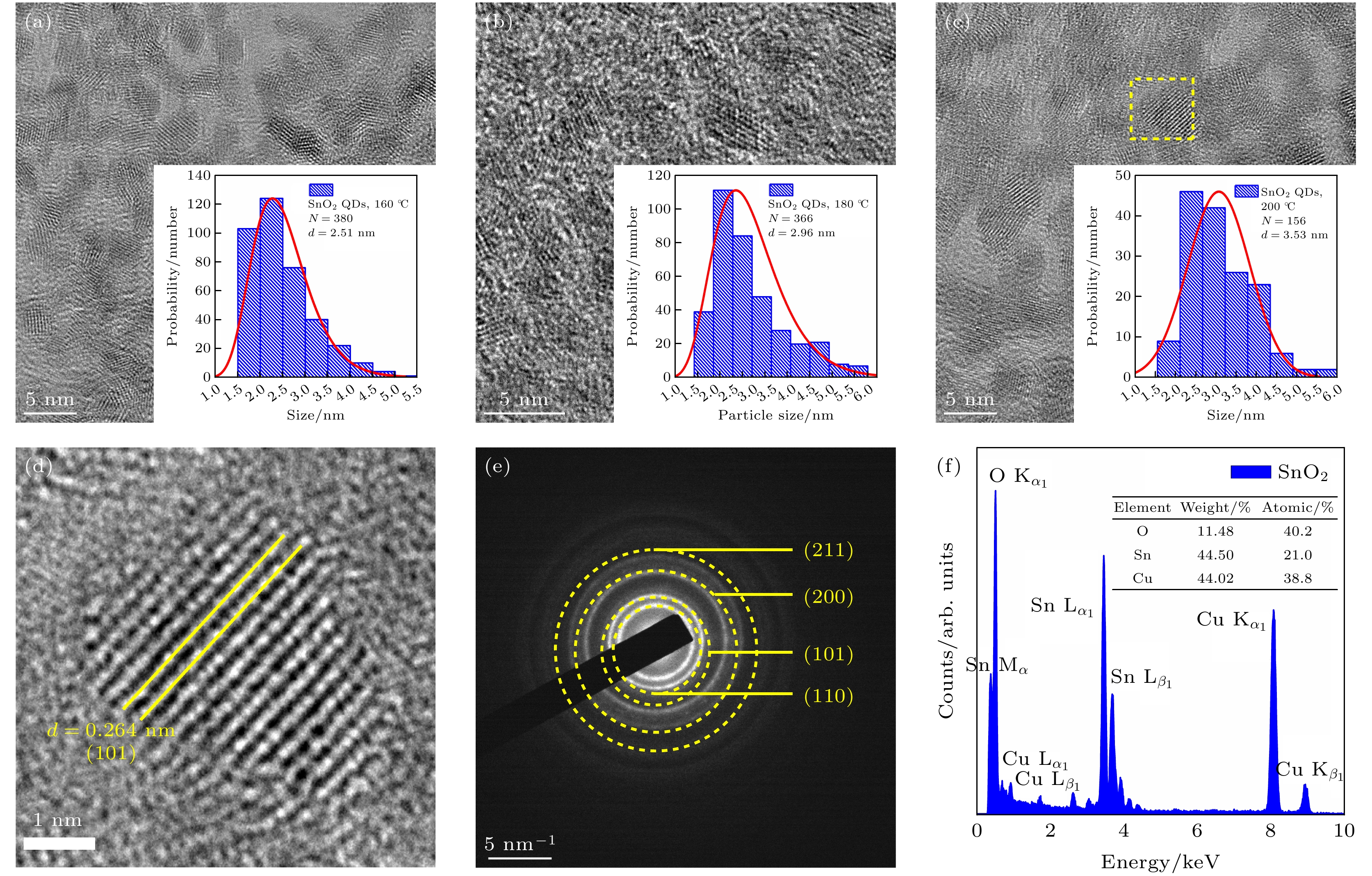
图 1 不同反应温度下制备的SnO2 QDs 的TEM图像 (a) 160 ℃; (b) 180 ℃; (c) 200 ℃. 插图分别为对应的SnO2 QDs尺寸分布直方图. 3.53 nm SnO2 QDs的(d)局部HRTEM图像, (e) 选区电子衍射图像与(f) EDS能谱分析
Figure 1. TEM images of SnO2 QDs prepared at (a) 160 ℃, (b) 180 ℃ and (c) 200 ℃. Inset gives the distribution histogram of SnO2 QDs size. (d) Magnified TEM image, (e) SAED pattern and (f) EDS spectrum of 3.53 nm SnO2 QDs.
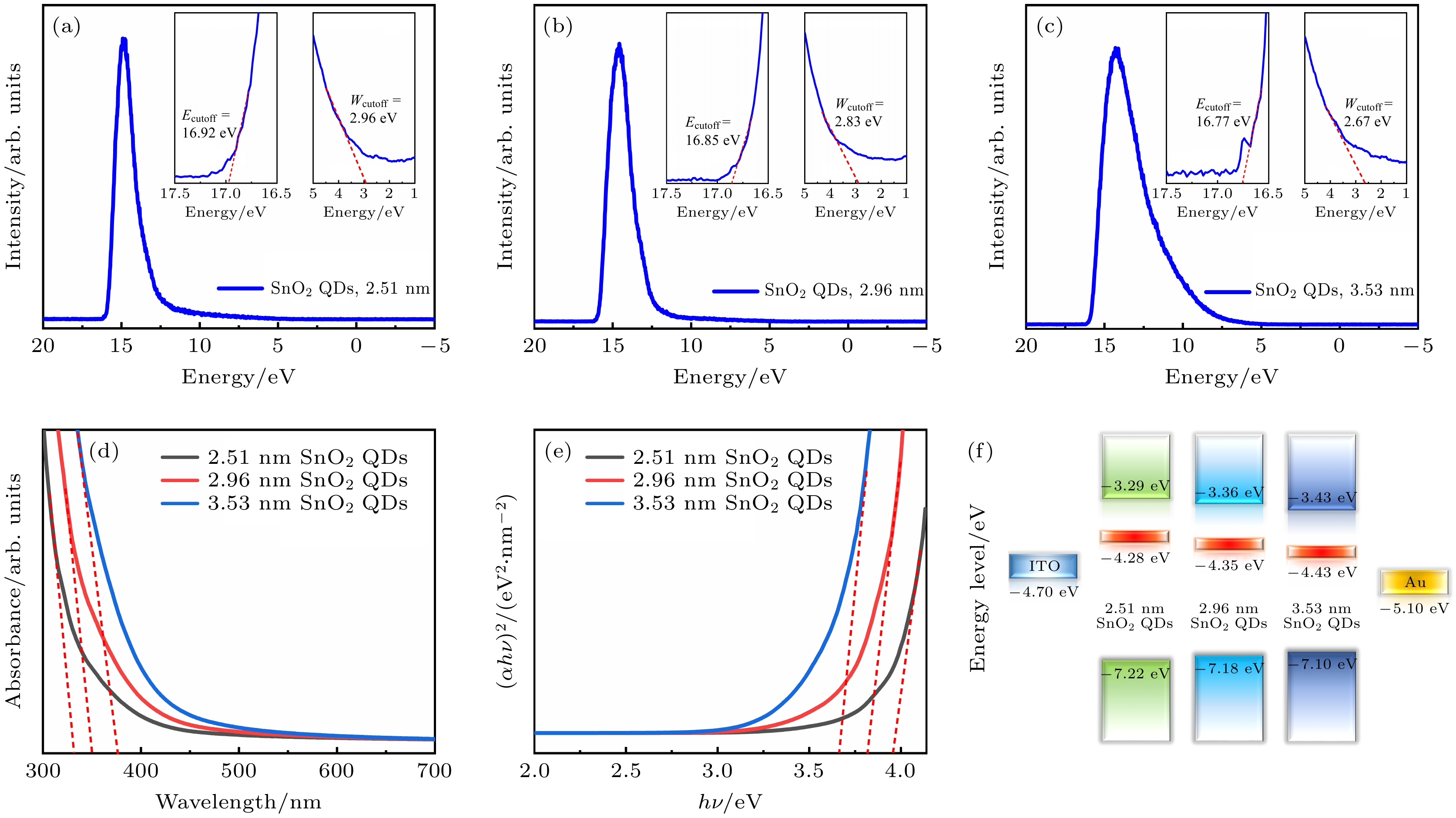
图 2 SnO2 QDs的UPS图谱 (a) 2.51 nm; (b) 2.96 nm; (c) 3.53 nm. 插图为费米边、二次电子截止边截距. 不同尺寸SnO2 QDs 的(d) UV-vis光谱, (e) 光学禁带曲线及(f) 能带结构示意图
Figure 2. UPS spectra of (a) 2.51 nm, (b) 2.96 nm and (c) 3.53 nm of SnO2 QDs, and insets shows the Secondary electron cutoff and Fermi edge intercepts. (d) UV-vis absorption spectra, (e) optical band gaps plots and (f) energy band structure of SnO2 QDs with different sizes.
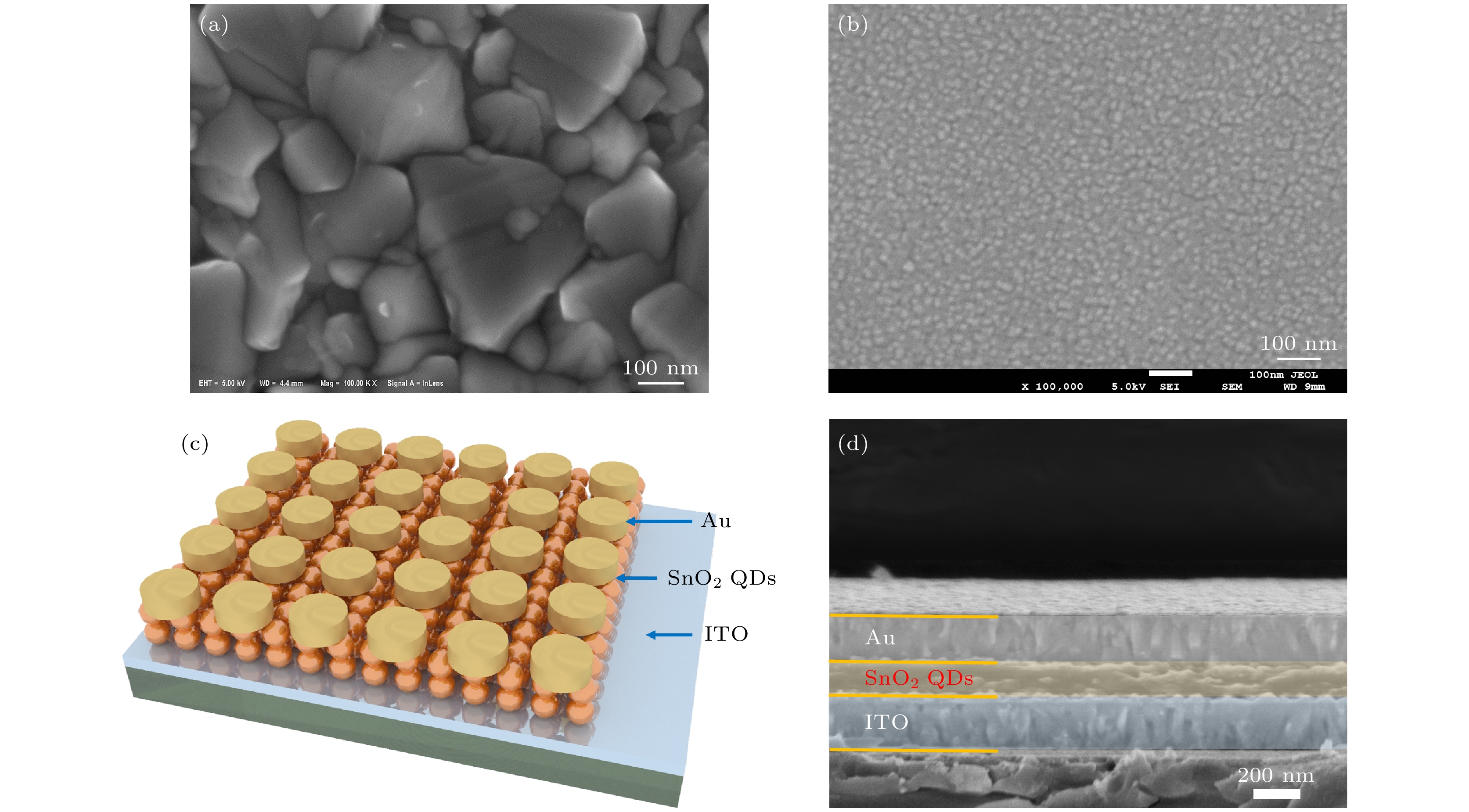
图 3 (a) ITO与(b) SnO2 QDs薄膜的表面SEM图像. (c) SnO2 QDs RRAM的器件结构示意图及(d) 横截面FESEM图像
Figure 3. Surface SEM picture of (a) ITO and (b) SnO2 QDs film. (c) Device structure schematic diagram of SnO2 QDs RRAM and its (d) cross-sectional FESEM image.
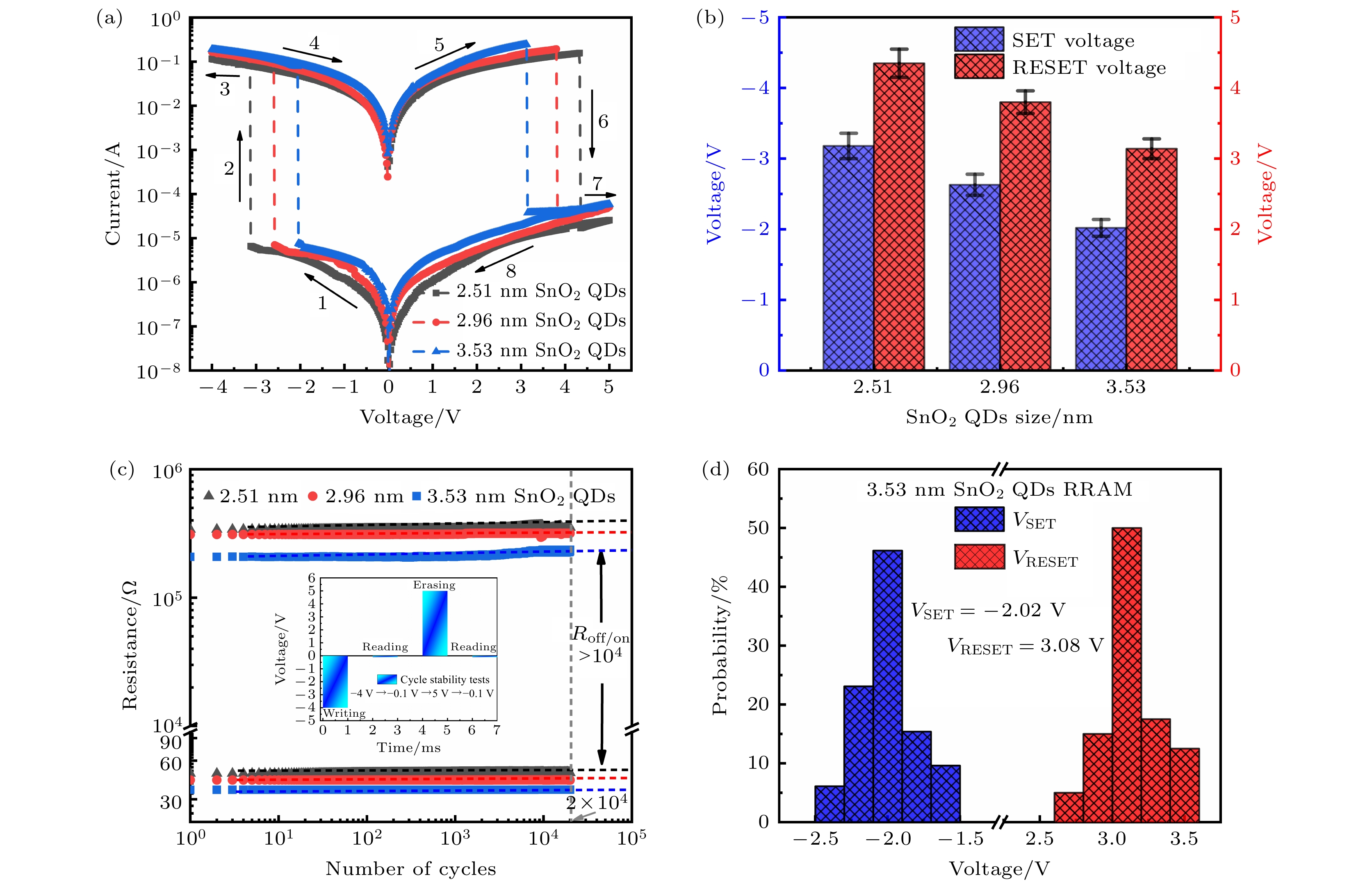
图 4 (a) 不同尺寸下SnO2 QDs RRAM的I-V特性曲线; (b) SET/RESET电压随SnO2 QDs尺寸的变化曲线; (c) 不同尺寸SnO2 QDs RRAM的循环稳定性曲线, 插图为施加的脉冲电压直方图; (d) 3.53 nm SnO2 QDs RRAM的SET/RESET电压频率分布直方图
Figure 4. (a) I-V curves of SnO2 QDs RRAM with different sizes; (b) variation of SET/RESET voltage with SnO2 QDs size; (c) cycle stability tests of SnO2 QDs RRAM and inset shows the impulse voltage curve; (d) SET/RESET voltage distribution of 3.53 nm SnO2 QDs RRAM.
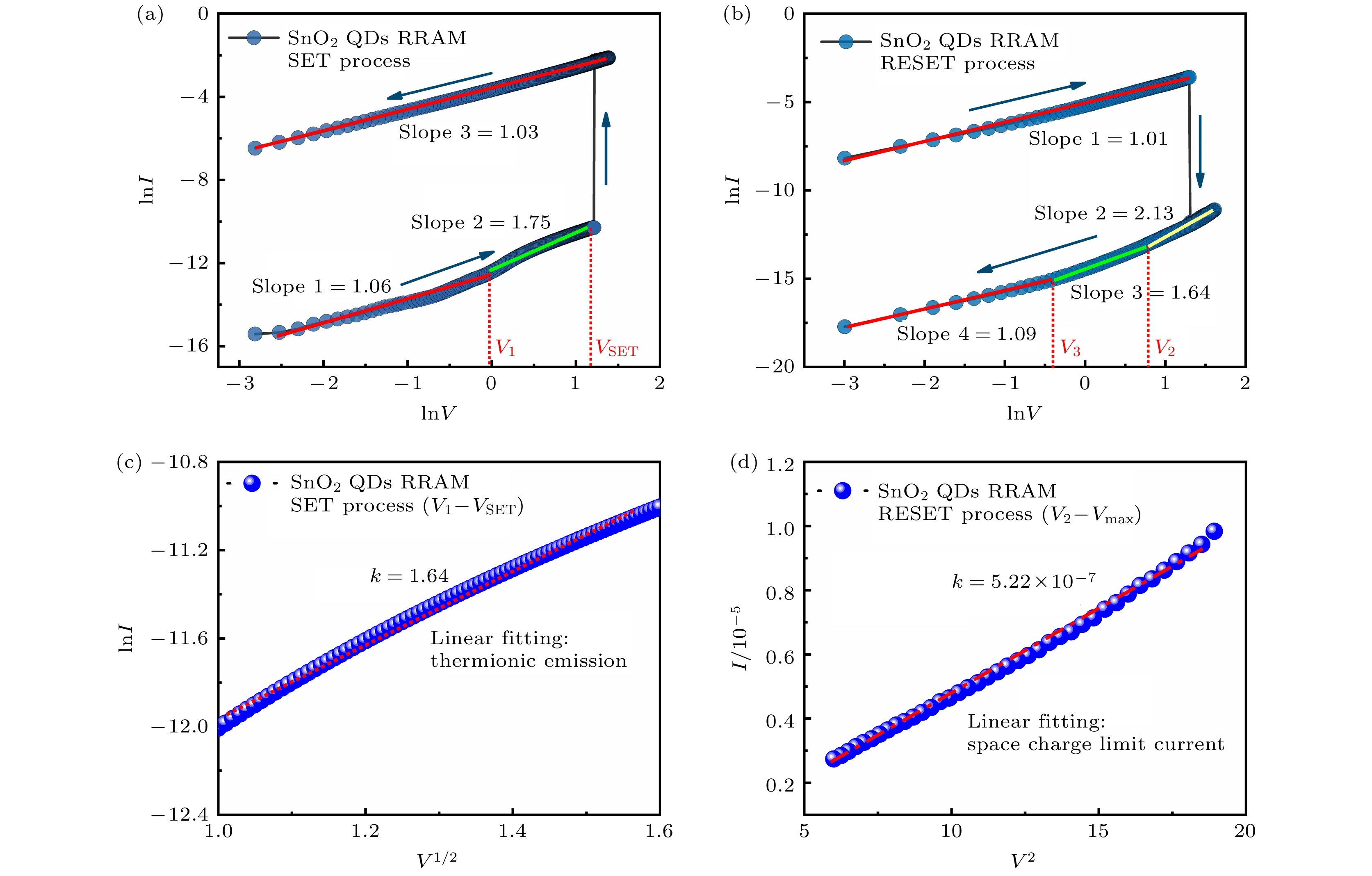
图 5 3.53 nm SnO2 QDs RRAM在(a) SET过程, (b) RESET过程的电导机制拟合曲线; 局部区域的电导机制拟合(c) SET过程V1-VSET阶段, (d) RESET过程V2-Vmax阶段
Figure 5. Conduction mechanism fitting curves of (a) SET process and (b) RESET process on 3.53 nm SnO2 QDs RRAM. Local region of conduction mechanism (c) stage of V1-VSET in SET process; (d) stage of V2-Vmax in RESET process.

图 6 (a) ITO/SnO2 QDs/Au界面势垒模型; 各阶段的阻变行为 (b) 热电子发射区域; (c) SET过程; (d) RESET过程; (e) SCLC区域; (f) RESET阶段热电子发射区域
Figure 6. (a) Schematic diagram of ITO/SnO2 QDs/Au interfacial barrier model and resistive switching behavior in (b) thermionic emission, (c) SET, (d) RESET, (e) SCLC, (f) thermionic emission of RESET process.
-
[1] Chen A 2016 Solid-State Electron. 125 25
Google Scholar
[2] Chang T C, Chang K C, Tsai T M, Chu T J, Sze S M 2016 Mater. Today 19 254
Google Scholar
[3] Li Y, Chu J, Duan W, Cai G, Fan X, Wang X, Wang G, Pei Y 2018 ACS Appl. Mater. Interfaces 10 24598
Google Scholar
[4] 史晨阳, 闵光宗, 刘向阳 2020 物理学报 69 178702
Google Scholar
Shi C Y, Min G Z, Liu X Y 2020 Acta Phys. Sin. 69 178702
Google Scholar
[5] Zhou G, Yang X, Xiao L, Sun B, Zhou A 2019 Appl. Phys. Lett. 114 163506
Google Scholar
[6] Gao S, Yi X, Shang J, Liu G, Li R W 2019 Chem. Soc. Rev. 48 1531
Google Scholar
[7] Zhou D, Chen F G, Han S, Hu W, Zang Z G, Hu Z P, Li S Q, Tang X S 2018 Ceram. Int. 44 S152
Google Scholar
[8] 孙劲鹏, 王太宏 2003 物理学报 52 2563
Google Scholar
Sun J P, Wang T H 2003 Acta Phys. Sin 52 2563
Google Scholar
[9] Datta S 2013 Quantum Transport: Atom to Transistor (England: Cambridge University Press) pp18, 170, 285
[10] Fan F, Zhang B, Cao Y, Yang X, Gu J, Chen Y 2017 Nanoscale 9 10610
Google Scholar
[11] Yan X, Pei Y, Chen H, Zhao J, Zhou Z, Wang H, Zhang L, Wang J, Li X, Qin C, Wang G, Xiao Z, Zhao Q, Wang K, Li H, Ren D, Liu Q, Zhou H, Chen J, Zhou P 2019 Adv. Mater. 31 1805284
Google Scholar
[12] Younis A, Chu D, Mihail I, Li S 2013 ACS Appl. Mater. Interfaces 5 9429
Google Scholar
[13] Wang Z Q, Liu Y L, Shen J, Chen W, Miao J, Li A, Liu K, Zhou J 2020 Sci. China Mater. 63 2497
Google Scholar
[14] Chen Z, Zhang Y, Yu Y, Cao M, Che Y, Jin L, Li Y, Li Q, Li T, Dai H, Yang J, Yao J 2019 Appl. Phys. Lett. 114 181103
Google Scholar
[15] Wang H, Yan X B 2019 Phys. Status Solidi RRL 13 1900073
Google Scholar
[16] Banerjee W, Liu Q, Long S B, Lv H B, Liu M 2017 J. Phys. D: Appl. Phys. 50 303002
Google Scholar
[17] Hwang B H, Lee J S 2018 Adv. Electron. Mater. 5 1800519
[18] 贾林楠, 黄安平, 郑晓虎, 肖志松, 王玫 2012 物理学报 61 217306
Google Scholar
Jia L N, Huang A P, Zheng X H, Xiao Z S, Wang M 2012 Acta Phys. Sin. 61 217306
Google Scholar
[19] Chen K Q, Zhou J, Chen W, Zhou P, He F, Liu Y L 2015 Part. Part. Syst. Char. 32 999
Google Scholar
[20] Chen D Y, Huang S H, Huang R, Zhang Q, Le T T, Cheng E, Hu Z J, Chen Z W 2018 Mater. Res. Lett. 6 462
Google Scholar
[21] Xu Z M, Guan P Y, Younis A, Chu D W, Li S 2017 RSC Adv. 7 56390
Google Scholar
[22] Sarkar P K, Bhattacharjee S, Prajapat M, Roy A 2015 RSC Adv. 5 105661
Google Scholar
[23] Shaalan N W, Hamad D, Abdel-Latief A Y, Abdel-Rahim M A 2016 Prog. Nat. Sci. 26 145
Google Scholar
[24] Onlaor K, Thiwawong T, Tunhoo B 2014 Org. Electron. 15 1254
Google Scholar
[25] Braun D 2010 J. Polym. Sci. Pol. Phys. 41 2622
[26] Zhang X G, Pantelides S T 2012 Phys. Rev. Lett. 108 266602
Google Scholar
[27] Valov I, Waser R, Jameson J R, Kozicki M N 2011 Nanotechnology 22 254003
Google Scholar
[28] Waser R, Dittmann R, Staikov G, Szot K 2009 Adv. Mater. 21 2632
Google Scholar
[29] Anoop G, Kim T Y, Lee H J, Panwar V, Kwak J H, Heo Y J, Yang J H, Lee J H, Jo J Y 2017 Adv. Electron. Mater. 3 1700264
Google Scholar
[30] Zhang P, Xu B, Gao C, Chen G L, Gao M Z 2016 ACS Appl. Mater. Interfaces 8 30336
Google Scholar
[31] Nieh C H, Lu M L, Weng T M, Chen Y F 2014 Appl. Phys. Lett. 104 1951
[32] 刘东青, 程海峰, 朱玄, 王楠楠, 张朝阳 2014 物理学报 63 187301
Google Scholar
Liu D Q, Cheng H F, Zhu X, Wang N N, Zhang C Y 2014 Acta Phys. Sin. 63 187301
Google Scholar
[33] Dash C S, Prabaharan S R S 2019 Rev. Adv. Mater. Sci. 58 248
Google Scholar
[34] Jeong J S, Topsakal M, Xu P, Jalan B, Wentzcovitch R M, Mkhoyan K A 2016 Nano Lett. 16 6816
Google Scholar
[35] Kumar A, Mukherjee S, Kranti A 2018 J. Phys. D: Appl. Phys. 51 405601
Google Scholar
[36] Hsu C C, Wang S Y, Lin Y S, Chen Y T 2018 J. Alloys Compd. 779 609
[37] Shi H P, Zheng J P, Cheng B C, Zhao J, Su X H, Xiao Y H, Lei S J 2017 J. Mater. Chem. C 5 229
Google Scholar
[38] Khan M T, Agrawal V, Almohammedi A, Gupta V 2018 Solid State Electron. 145 49
Google Scholar
[39] Mei F, Shen H, Li L B, Zang G Z, Zhou M, Ti R X, Yang D Y, Huang F Z, Lu X M, Zhu J S 2017 Appl. Phys. Lett. 111 143503
Google Scholar
[40] Liu Y, Guo J, Zhu E B, Liao L, Lee S J, Ding M N, Shakir I, Gambin V, Huang Y, Duan X F 2018 Nature 557 696
Google Scholar

 DownLoad:
Catalog
Metrics
- Abstract views: 3875
- PDF Downloads: 82
- Cited By: 0
