


-
The development of terahertz (THz) technology is creating a demand for devices that can modulate THz beams. Here, we propose a novel THz modulator based on patterned graphene/gallium nitride Schottky diodes hybridized with metasurfaces. Ultrasensitive dynamic multidimensional THz modulation is achieved by changing the Schottky barrier of the heterojunction, shifting the Fermi level between the Dirac point, changing the conduction band and the valence of graphene via continuous-wave optical illumination or bias voltages. When the Fermi level is close to the Dirac point, the modulation is ultrasensitive to the external stimuli. Applying an optical power of 4.9–162.4 mW/cm2 or a bias voltage of 0.5–7.0 V, the modulation depth initially increases, then decreases, and the phase difference linearly increases, therein the maximum modulation depth is 90%, and the maximum phase difference is 189°. In short, the proposed THz modulator has potential application in ultra-sensitive optical devices.
-
Keywords:
- terahertz metasurfaces /
- modulator /
- Schottky diodes /
- graphene
[1] Manjappa M, Srivastava Y K, Solanki A, Kumar A, Sum T C, Singh R 2017 Adv. Mater. 29 1605881
 Google Scholar
[2] Yao H, Yan X, Yang M, Yang Q, Liu Y, Li A, Wang M, Wei D, Tian Z, Liang L 2021 Carbon 184 400
Google Scholar
[3] Yang M, Li T, Gao J, Yan X, Liang L, Yao H, Li J, Wei D, Wang M, Zhang T, Ye Y, Song X, Zhang H, Ren Y, Ren X, Yao J 2021 Appl. Surf. Sci. 562 150182
Google Scholar
[4] Tan T C, Srivastava Y K, Ako R T, Wang W, Bhaskaran M, Sriram S, Al Naib I, Plum E, Singh R 2021 Adv. Mater. 33 2100836
Google Scholar
[5] Zhang J, Mu N, Liu L, Xie J, Feng H, Yao J, Chen T, Zhu W 2021 Biosens. Bioelectron. 185 113241
Google Scholar
[6] 闫昕, 梁兰菊, 张雅婷, 丁欣, 姚建铨 2015 物理学报 64 158101
Google Scholar
Yan X, Liang L J, Zhang Y T, Ding X, Yao J Q 2015 Acta Phys. Sin. 64 158101
Google Scholar
[7] 闫昕, 梁兰菊, 张璋, 杨茂生, 韦德泉, 王猛, 李院平, 吕依颖, 张兴坊, 丁欣, 姚建铨 2018 物理学报 67 118102
Google Scholar
Yan X, Liang L J, Zhang Z, Yang M S, Wei D Q, Wang M, Li Y P, Lü Y Y, Zhang X F, Ding X, Yao J Q 2018 Acta Phys. Sin. 67 118102
Google Scholar
[8] Cheng Y, Zhang K, Liu Y, Li S, Kong W 2020 AIP Adv. 10 045026
Google Scholar
[9] Li C, Li W, Duan S, Wu J, Chen B, Yang S, Su R, Jiang C, Zhang C, Jin B B 2021 Appl. Phys. Lett. 119 052602
Google Scholar
[10] Xiao S, Wang T, Liu T, Yan X, Li Z, Xu C 2018 Carbon 126 271
Google Scholar
[11] Driscoll T, Kim H T, Chae B G, Leen Y W, Jokersts N M, Palit S, Smith D R, Ventra M D, Basov D N 2009 Science 325 1518
Google Scholar
[12] Chen H T, O'Hara J F, Azad A K, Taylor A J, Averitt R D, Shrekenhamer D B, Padilla W J 2008 Nat. Photonics 2 295
Google Scholar
[13] Ghosh S K, Das S, Bhattacharyya S 2021 Opt. Commun. 480 126480
Google Scholar
[14] Choi W, Lahiri I, Seelaboyina R, Kang Y S 2010 Crit. Rev. Solid State Mater. Sci. 35 52
Google Scholar
[15] Feng J, Li W, Qian X, Qi J, Qi L, Li J 2012 Nanoscale 4 4883
Google Scholar
[16] Yang G, Li L, Lee W B, Ng M C 2018 Sci. Technol. Adv. Mater. 19 613
Google Scholar
[17] Wei T, Bao L, Hauke F, Hirsch A 2020 ChemPlusChem 85 1655
Google Scholar
[18] Shukla S, Kang S Y, Saxena S 2019 Appl. Phys. Rev. 6 021311
Google Scholar
[19] Lee S H, Choi M, Kim T T, Seungwoo L, Liu M, Yin X, Choi H, Lee S, Choi C G, Choi S Y, Zhang X, Min B 2012 Nat. Mater. 11 936
Google Scholar
[20] Li Q, Gupta M, Zhang X, Wang S, Chen T, Singh R, Han J, Zhang W 2020 Adv. Mater. 5 1900840
Google Scholar
[21] Kim S, Seo T H, Kim M J, Song K M, Suh E K, Kim H 2015 Nano. Res. 8 1327
Google Scholar
[22] Bartolomeo A D 2016 Phys. Rep. 606 1
Google Scholar
[23] Xu G, Zhang Y, Duan X, Balandin A A, Wang K L 2013 Proc. IEEE 101 1670
Google Scholar
[24] Liu N, Langguth L, Weiss T, Kastel J, Fleischhauer M, Pfau T, Giessen H 2009 Nat. Mater. 8 758
Google Scholar
[25] Chen H, Zhang H, Zhao Y, Liu S, Cao M, Zhang Y 2018 Opt. Laser Technol. 104 210
Google Scholar
[26] Ryzhii V, Ryzhii M, Otsuji T, Leiman V, Mitin V, Shur M S 2021 J. Appl. Phys. 129 214503
Google Scholar
[27] Ryzhii V, Otsuji T, Ryzhii M, Leiman V G, Maltsev P P, Karasik V E, Mitin V, Shur M S 2021 Opt. Mater. Express 11 468
Google Scholar
[28] Jessop D S, Kindness S J, Xiao L, Braeuninger P W, Lin H, Ren Y, Ren C X, Hofmann S, Zeitler J A, Beere H E, Ritchie D A, Degl’Innocenti R 2016 Appl. Phys. Lett. 108 171101
Google Scholar
-
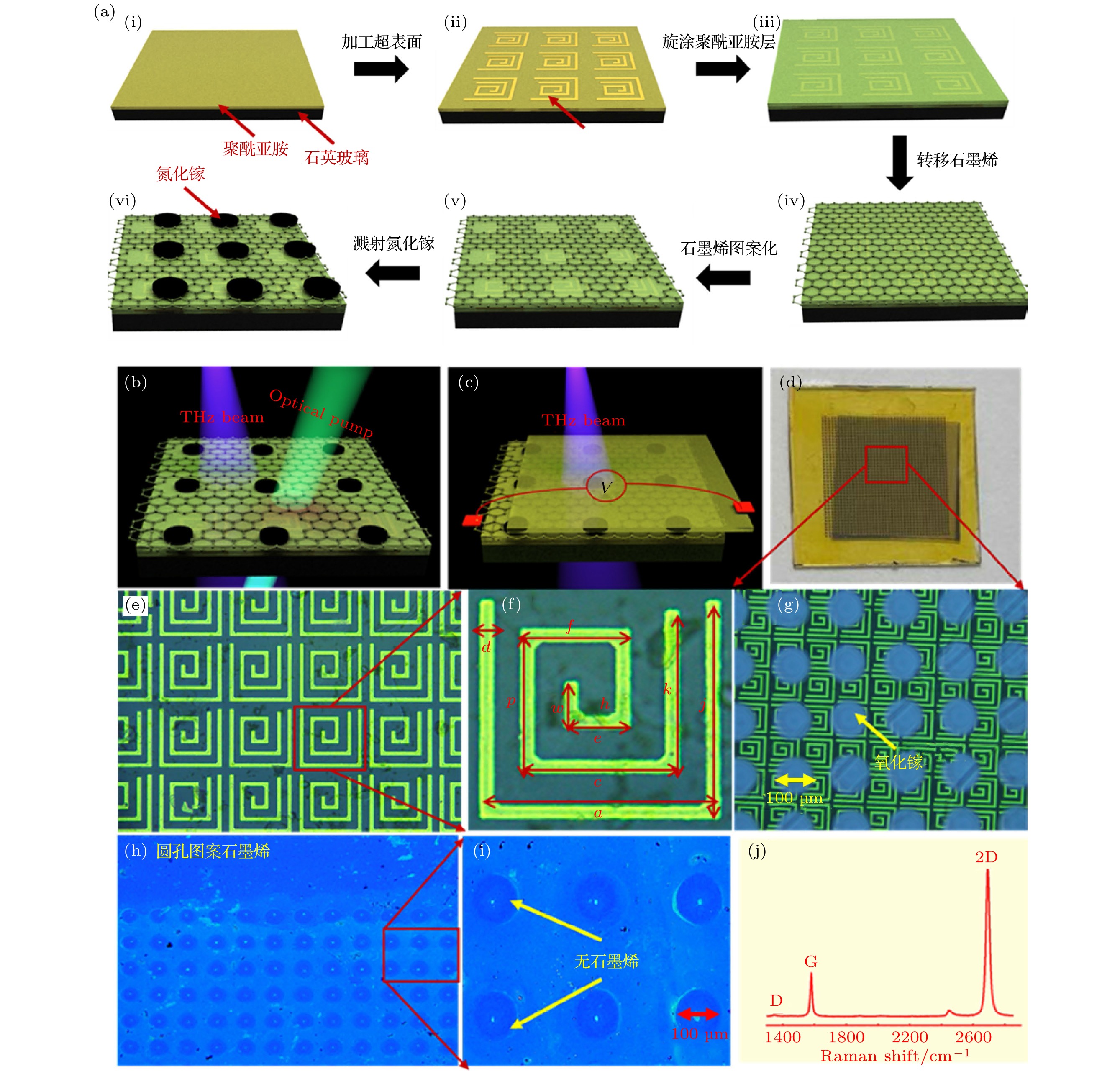
图 1 PGrGAN@MS的制备和表征 (a)制备过程: (i) PI膜旋涂在石英玻璃基地上; (ii)类 EIT 超表面的制备; (iii) PI膜旋涂在类EIT超表面上; (iv) 石墨烯被转移到 PI 薄膜上; (v) 图案化单层石墨烯; (vi)溅射圆柱状氮化镓. (b)在光泵和太赫兹激发下的样品示意图. (c)在偏置电压和太赫兹激发下的样品示意图. (d) 1.5 cm × 1.5 cm PGrGAN@MS样品. (e)超表面的光学显微镜照片. (f)晶胞尺寸, a = j = 135 µm, d = 13 µm, c = p = 90 µm, k = 103 µm, f = h = 63 µm, e = 39 mm, w = 31 mm. (g)样品的光学显微照片. (h), (i)圆孔石墨烯图案化结构的光学显微照片. (j)使用514 nm激光测量的石英衬底上单层石墨烯的拉曼光谱
Figure 1. Manufacture and characterization of the PGrGAN@MS. (a) Manufacture process: (i) PI film is spin-coated on the quartz glass substrate; (ii) preparation of an EIT-like metasurface sample; (iii) PI film is spin-coated atop metasurface; (iv) graphene was transferred onto the PI film; (v) graphene was patterned into a fishing net structure with round holes; (vi) sputtering cylindrical GaN. (b), (c) Schematic of graphene samples under the optical pump or bias voltages and THz probe illumination. (d) 1.5 cm × 1.5 cm PGrGAN@MS sample. (e) Optical microscope images of lattice. (f) Unit cell. The corresponding parameters were: a = j = 135 µm, d = 13 µm, c = p = 90 µm, k = 103 µm, f = h = 63 µm, e = 39 mm, w = 31 mm. (g) Optical microscope images of the sample. (h), (i) Optical micrograph of the patterned structure of round-hole graphene. (j) Raman spectrum of monolayer graphene on quartz substrate measured by 514 nm laser.
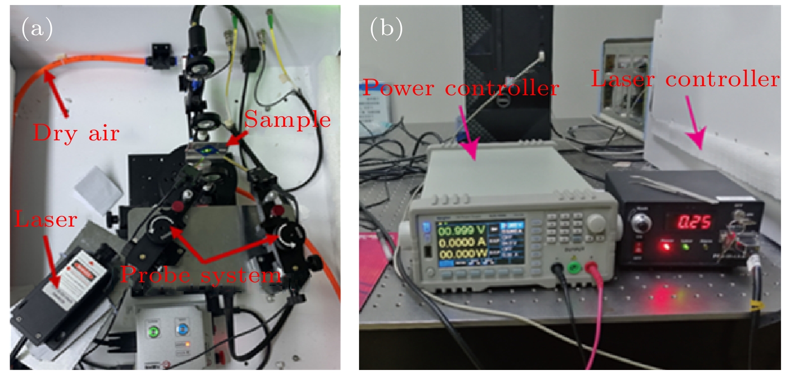
图 2 实验光电设备 (a) THz-TDs系统; (b) 室温下的电源和激光控制器
Figure 2. Experimental photoelectric equipment: (a) THz-TDs system; (b) power supply and laser controller at room temperature.

图 3 (a), (b) 在NSZ和WPX的共振频率处电场强度分布; (c)在0.63 THz谐振频率下EIT模式的电场强度分布; (d)实验、模拟和理论拟合的透射光谱
Figure 3. (a), (b) Electric field intensity distribution at the resonance frequency of NSZ and WPX; (c) electric field intensity distribution of the EIT mode at the resonance frequency of 0.63 THz; (d) experimental, simulated and theory fitted transmission spectra.
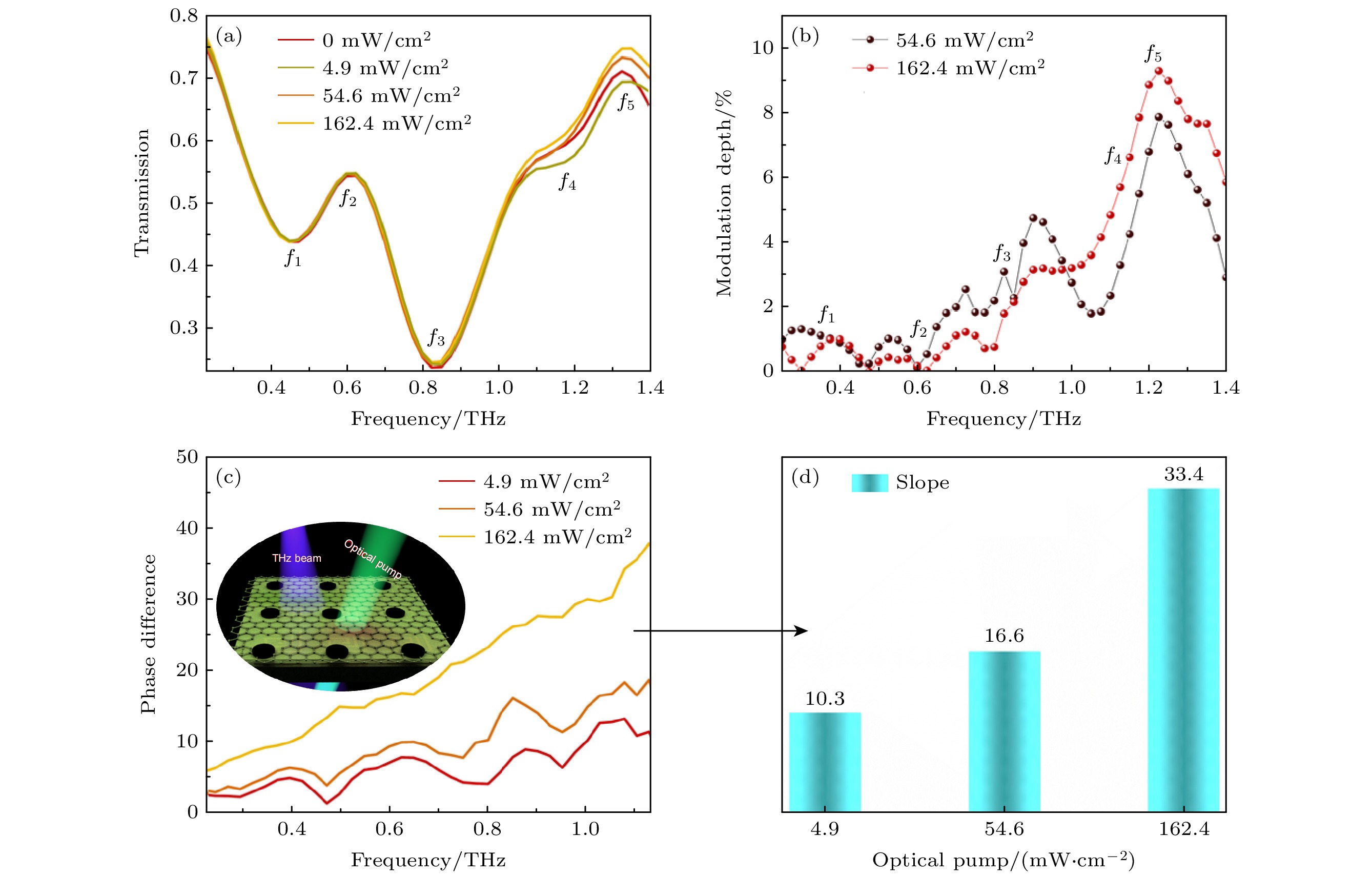
图 4 (a) PGrGAN@MS样品在不同光通量激发下的太赫兹透射谱线; (b) PGrGAN@MS样品在不同光通量激发下的调制深度; (c) PGrGAN@MS样品在光通量激发与没有任何激发条件下的相位差(内插图为激发方式); (d) PGrGAN@MS样品在不同光通量激发下的相位差的斜率
Figure 4. (a) Measured transmission amplitude spectra of the PGrGAN@MS sample under different optical flux (Fop) excitations; (b) modulation depth of the PGrGAN@MS sample under different Fop excitations from panel (a); (c) phase difference between the PGrGAN@MS sample with and without Fop excitations, inset: excitation approach; (d) fitted phase difference slopes on Fop excitations extracted from panel (c).

图 5 (a) PGrGAN@MS样品在不同偏置电压激发下的太赫兹透射谱线; (b) PGrGAN@MS样品在不同偏置电压激发下的调制深度; (c) PGrGAN@MS样品在偏置电压激发与没有任何激发条件下的相位差(内插图为激发方式); (d) PGrGAN@MS样品在不同偏置电压激发下的相位差的斜率
Figure 5. (a) Measured transmission amplitude spectra of the PGrGAN@MS sample under different Vb excitations; (b) modulation depth of the PGrGAN@MS sample under different Vb excitations from panel (a); (c) phase difference between the PGrGAN@MS sample with and without Vb excitations, inset: excitation approach; (d) fitted phase difference slopes on Vb excitations extracted from panel (c).

图 6 PGrGAN@MS样品在(a)没有任何激发、(b)光激发以及(c)电激发三种不同情况下的异质结能带结构示意图
Figure 6. Schematic band structures of the PGrGAN@MS sample (a) without any excitation in darkness, (b) light excitation and (c) electrical excitation.
-
[1] Manjappa M, Srivastava Y K, Solanki A, Kumar A, Sum T C, Singh R 2017 Adv. Mater. 29 1605881
Google Scholar
[2] Yao H, Yan X, Yang M, Yang Q, Liu Y, Li A, Wang M, Wei D, Tian Z, Liang L 2021 Carbon 184 400
Google Scholar
[3] Yang M, Li T, Gao J, Yan X, Liang L, Yao H, Li J, Wei D, Wang M, Zhang T, Ye Y, Song X, Zhang H, Ren Y, Ren X, Yao J 2021 Appl. Surf. Sci. 562 150182
Google Scholar
[4] Tan T C, Srivastava Y K, Ako R T, Wang W, Bhaskaran M, Sriram S, Al Naib I, Plum E, Singh R 2021 Adv. Mater. 33 2100836
Google Scholar
[5] Zhang J, Mu N, Liu L, Xie J, Feng H, Yao J, Chen T, Zhu W 2021 Biosens. Bioelectron. 185 113241
Google Scholar
[6] 闫昕, 梁兰菊, 张雅婷, 丁欣, 姚建铨 2015 物理学报 64 158101
Google Scholar
Yan X, Liang L J, Zhang Y T, Ding X, Yao J Q 2015 Acta Phys. Sin. 64 158101
Google Scholar
[7] 闫昕, 梁兰菊, 张璋, 杨茂生, 韦德泉, 王猛, 李院平, 吕依颖, 张兴坊, 丁欣, 姚建铨 2018 物理学报 67 118102
Google Scholar
Yan X, Liang L J, Zhang Z, Yang M S, Wei D Q, Wang M, Li Y P, Lü Y Y, Zhang X F, Ding X, Yao J Q 2018 Acta Phys. Sin. 67 118102
Google Scholar
[8] Cheng Y, Zhang K, Liu Y, Li S, Kong W 2020 AIP Adv. 10 045026
Google Scholar
[9] Li C, Li W, Duan S, Wu J, Chen B, Yang S, Su R, Jiang C, Zhang C, Jin B B 2021 Appl. Phys. Lett. 119 052602
Google Scholar
[10] Xiao S, Wang T, Liu T, Yan X, Li Z, Xu C 2018 Carbon 126 271
Google Scholar
[11] Driscoll T, Kim H T, Chae B G, Leen Y W, Jokersts N M, Palit S, Smith D R, Ventra M D, Basov D N 2009 Science 325 1518
Google Scholar
[12] Chen H T, O'Hara J F, Azad A K, Taylor A J, Averitt R D, Shrekenhamer D B, Padilla W J 2008 Nat. Photonics 2 295
Google Scholar
[13] Ghosh S K, Das S, Bhattacharyya S 2021 Opt. Commun. 480 126480
Google Scholar
[14] Choi W, Lahiri I, Seelaboyina R, Kang Y S 2010 Crit. Rev. Solid State Mater. Sci. 35 52
Google Scholar
[15] Feng J, Li W, Qian X, Qi J, Qi L, Li J 2012 Nanoscale 4 4883
Google Scholar
[16] Yang G, Li L, Lee W B, Ng M C 2018 Sci. Technol. Adv. Mater. 19 613
Google Scholar
[17] Wei T, Bao L, Hauke F, Hirsch A 2020 ChemPlusChem 85 1655
Google Scholar
[18] Shukla S, Kang S Y, Saxena S 2019 Appl. Phys. Rev. 6 021311
Google Scholar
[19] Lee S H, Choi M, Kim T T, Seungwoo L, Liu M, Yin X, Choi H, Lee S, Choi C G, Choi S Y, Zhang X, Min B 2012 Nat. Mater. 11 936
Google Scholar
[20] Li Q, Gupta M, Zhang X, Wang S, Chen T, Singh R, Han J, Zhang W 2020 Adv. Mater. 5 1900840
Google Scholar
[21] Kim S, Seo T H, Kim M J, Song K M, Suh E K, Kim H 2015 Nano. Res. 8 1327
Google Scholar
[22] Bartolomeo A D 2016 Phys. Rep. 606 1
Google Scholar
[23] Xu G, Zhang Y, Duan X, Balandin A A, Wang K L 2013 Proc. IEEE 101 1670
Google Scholar
[24] Liu N, Langguth L, Weiss T, Kastel J, Fleischhauer M, Pfau T, Giessen H 2009 Nat. Mater. 8 758
Google Scholar
[25] Chen H, Zhang H, Zhao Y, Liu S, Cao M, Zhang Y 2018 Opt. Laser Technol. 104 210
Google Scholar
[26] Ryzhii V, Ryzhii M, Otsuji T, Leiman V, Mitin V, Shur M S 2021 J. Appl. Phys. 129 214503
Google Scholar
[27] Ryzhii V, Otsuji T, Ryzhii M, Leiman V G, Maltsev P P, Karasik V E, Mitin V, Shur M S 2021 Opt. Mater. Express 11 468
Google Scholar
[28] Jessop D S, Kindness S J, Xiao L, Braeuninger P W, Lin H, Ren Y, Ren C X, Hofmann S, Zeitler J A, Beere H E, Ritchie D A, Degl’Innocenti R 2016 Appl. Phys. Lett. 108 171101
Google Scholar

 DownLoad:
Catalog
Metrics
- Abstract views: 4017
- PDF Downloads: 125
- Cited By: 0
