


-
Shielded gate trench metal-oxide-semiconductor field effect transistor (SGT-MOSFET) introduces a longitudinal shielding gate connected to the source inside the body, which can assist in depleting the drift region. Its principle of withstanding voltage is different from that of the vertical U-groove MOSFET (VUMOSFET). The SGT-MOSFET will generate two electric field peaks inside the body, which will further optimize the electric field strength distribution of the device and increase the breakdown voltage of the device. Therefore, SGT-MOSFET has not only the advantages of low conduction loss of CCMOSFET, but also lower switching loss. The effects of structural parameters such as the width of the mesa, the thickness of the field oxygen, the depth of the trench and the doping concentration on the electric field strength distribution of SGT-MOSFET are not independent of each other. The more the parameters, the more complex the correlation of their effects on the electric field strength distribution is. In this paper, we take 110V SGT-MOSFET as a research object. Through numerical simulation, theoretical analysis and analytical modeling, the principle of withstanding voltage for different structures and the correlation between structural parameters and electric field strength distribution are studied. The analytical model of the electric field related to various structural parameters of the device is established, which provides a theoretical basis for the design of the device structure. The analytical model of electric field under low current is modified by introducing avalanche carriers, so that the modified analytical results can better match the simulation results. Through the modified electric field analysis model, the field oxygen thicknessin an optimal electric field is 0.68 µm . Comparing with the product of SGTMOSFET with 0.58 µm field oxygen thickness, at the optimal field oxygen thickness of 0.68 µm, the on-resistance of the device is reduced because the on-area of the device is increased; the electric field distribution is more uniform, so the device breakdown voltage increases; the gate-source capacitance decreases and the gate-drain capacitance is almost no change, so the gate-source charge decreases and the gate-drain charge is almost no change, while the total gate charge decreases. As a result, the optimal value parameter FOM1 of the device is increased by 18.9%, and the optimal value parameter FOM2 is reduced by 8.5%. Therefore, the static and dynamic characteristics of the device are significantly promoted, and the performance of the corresponding products is greatly improved.
[1] Nguyen M H, Kwak S 2020 Electronics 9 2068
 Google Scholar
[2] Huang A Q 2017 P. IEEE. 105 2019
Google Scholar
[3] Krishnan R 2020 IEEE Ind. Electron. Mag. 16 105
[4] Williams R K, Darwish M N, Blanchard R A, Siemieniec R, Rutter P, Kawaguchi Y 2017 IEEE. T. Electron. Dev. 64 692
Google Scholar
[5] Xi J, Wang J, Lu J, Chen J, Xin Y, Li Z, Tu C, Shen Z J 2018 Microelectron. Reliab. 88–90 593
[6] Park C, Havanur S, Shibib A, Terrill K 2016 Proceedings of the 28th International Symposium on Power Semiconductor Devices and ICs Prague, Czech Republic, June 12–16, 2016 p387
[7] Wang Y, Hu H F, Jiao W 2012 IEEE. T. Electron. Dev. 59 3037
Google Scholar
[8] Tian Y, Yang Z, Xu Z, Liu S, Sun W F, Shi L, Zhu Y, Ye P, Zhou J 2018 Superlattice. Microst. 116 151
Google Scholar
[9] Su L, Wang C L, Yang W H, An J 2022 Microelectron. Reliab. 139 114822
Google Scholar
[10] Tong C F, Mawby P A, Covington J A 2009 13th European Conference on Power Electronics and Applications Barcelona, Spain, September 8–10, 2009 10939294
[11] Wang Y, Yu C H, Hu H F, Dou Z 2013 IET. Power. Electron. 7 2964
[12] Wang Y, Lan H, Dou Z, Hu H F 2014 IET. Power. Electron. 7 2030
Google Scholar
[13] Deng S, Hossain Z, Taniguchi T 2017 IEEE. T. Electron. Dev. 64 735
Google Scholar
[14] Wang W, Ning R, Shen Z J 2017 IEEE. Electr. Device. L. 38 1055
Google Scholar
[15] Chien F T, Wang Z Z, Lin C L, Kang T K, Chen C W, Chiu H C 2020 Micromachines 11 504
Google Scholar
[16] Chen R, Wang L, Jiu N, Zhang H, Guo, M 2020 Electronics 9 745
Google Scholar
[17] Wang Z K, Qiao M, Fang D, Wang R D, Qi Z, Li Z J, Zhang B 2020 IEEE. Electr. Device. L. 41 749
Google Scholar
[18] Su L, Wang C L, Yang W H, Zhang C 2023 Microelectron. Reliab. 143 114950
Google Scholar
[19] Zhang W T, Pu S, Lai C L, Ye L, Cheng S, Zhang S, He B, Wang Z, Luo X, Qiao M 2018 Proceedings of the 30th International Symposium on Power Semiconductor Devices and ICs Chicago, IL, USA, May 13–17, 2018 p475
[20] Zhang W T, Ye L, Fang D, Qiao M, Xiao K, He B Y, Li Z J, Zhang B 2019 IEEE. T. Electron. Dev. 66 1416
Google Scholar
[21] Zhang W T, Zhang B, Qiao M, Wu L J, Mao K, Li Z J 2014 IEEE. T. Electron. Dev. 61 518
Google Scholar
[22] Oetjen J, Jungblut R, Kuhlmann U, Arkenau J, Sittig R 2000 Solid. State. Electronic. 44 117
Google Scholar
[23] Jacoboni C, Canali C, Ottaviani G, Quaranta A A 1977 Solid. State. Electronic. 20 77
Google Scholar
-
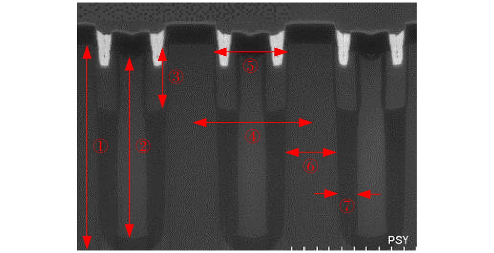
图 1 SGT-MOSFE产品SEM图
Figure 1. The SEM photo of SGT-MOSFE product.
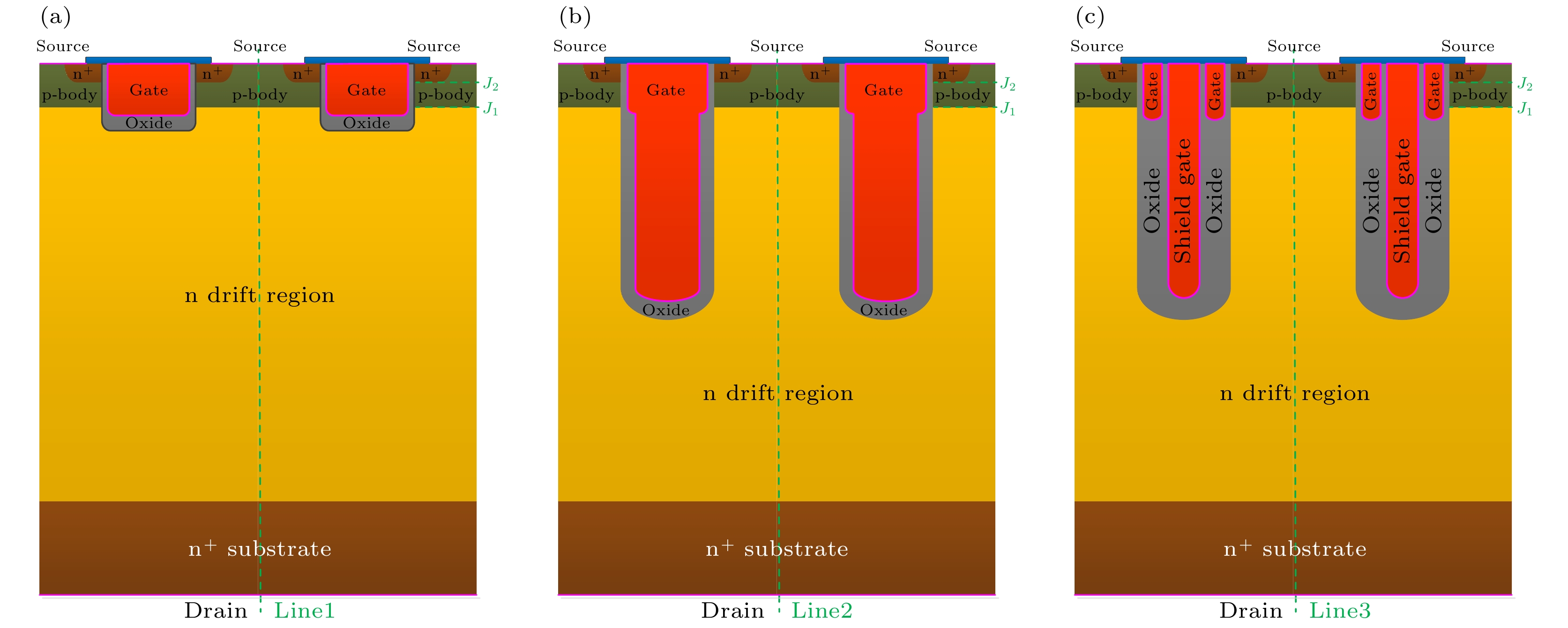
图 2 两元胞VUMOSFET (a), CCMOSFET (b), SGT-MOSFET (c)结构图
Figure 2. The structures of two-cell VUMOSFET (a), CCMOSFET (b), SGT - MOSFET (c).
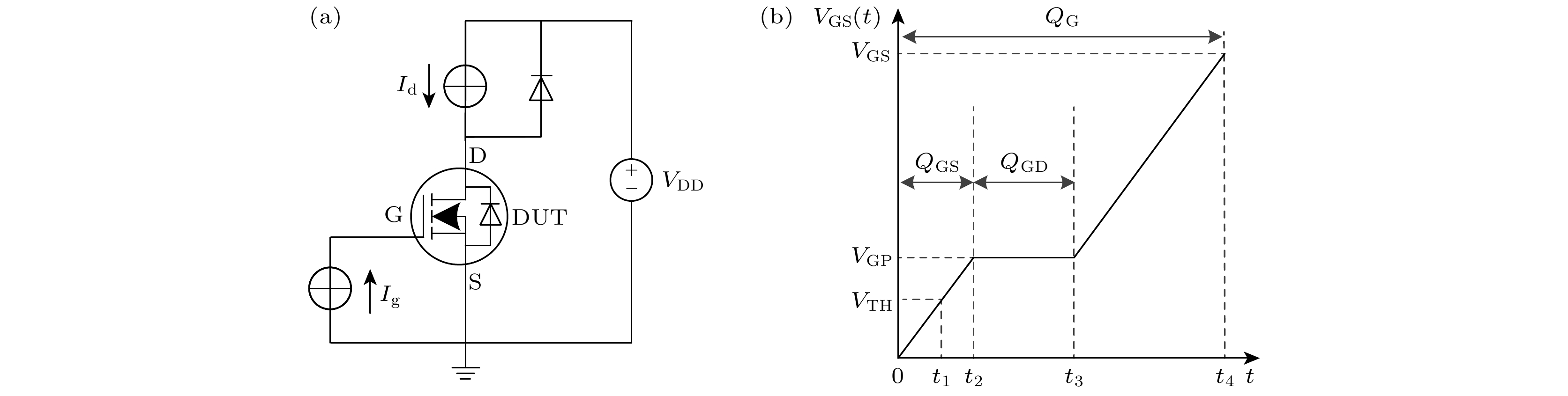
图 3 (a)栅电荷测试电路; (b) 栅电荷测试波形
Figure 3. (a) Testing circuit of the gate charge; (b) test waveform of the gate charge.
图 4 不同结构击穿曲线对比
Figure 4. Comparison of breakdown curves of different structures.
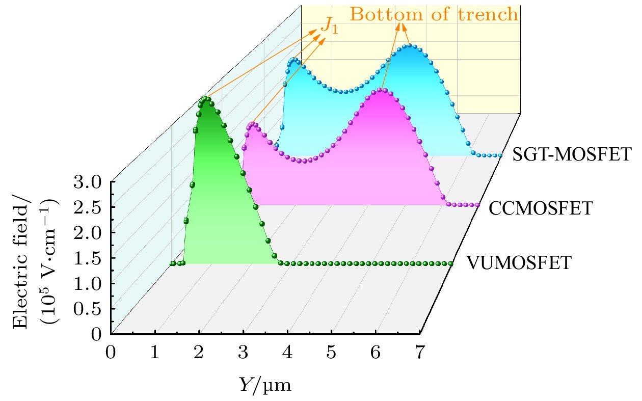
图 5 不同结构电场强度分布图
Figure 5. The electric field strength distribution diagram of different structures.

图 6 不同结构电势分布曲线
Figure 6. The potential distribution curves of different structures.
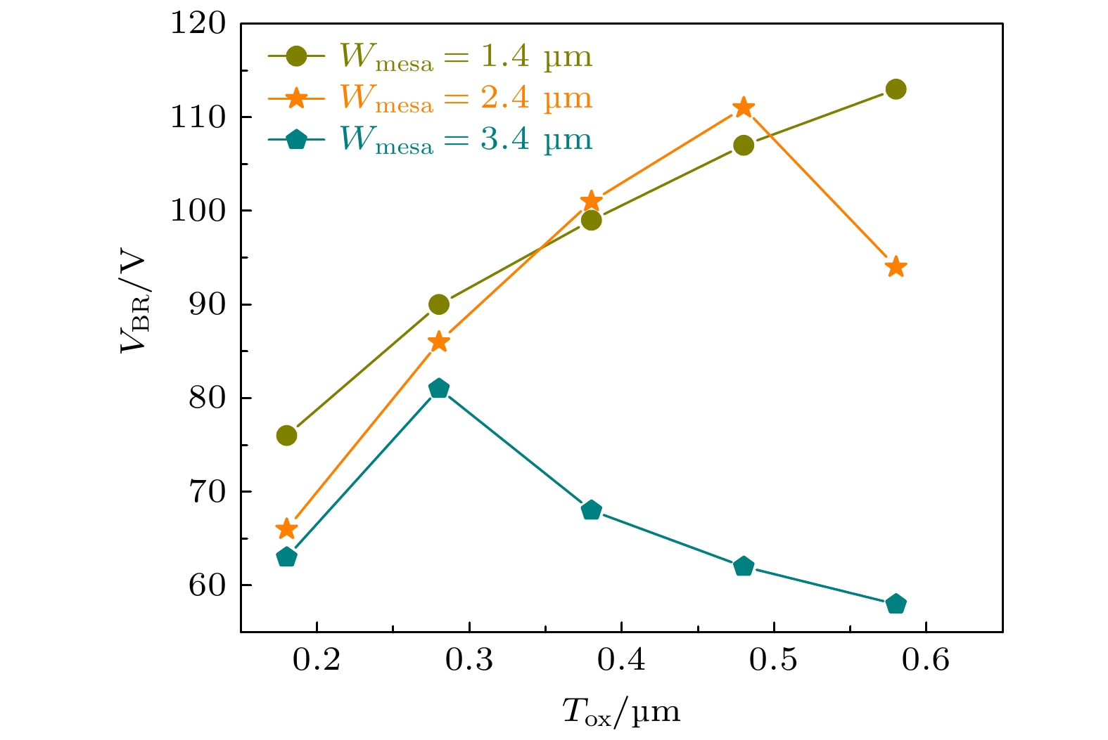
图 7 不同场氧厚度下的击穿电压
Figure 7. The breakdown voltage under different field oxygen thicknesses.
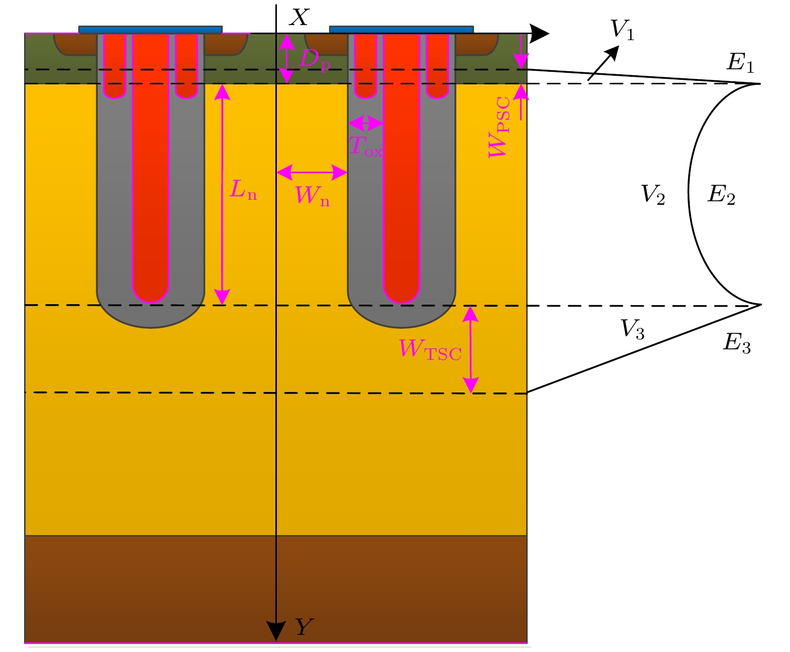
图 8 SGT-MOSFET结构示意图
Figure 8. The schematic diagram of SGT-MOSFET.
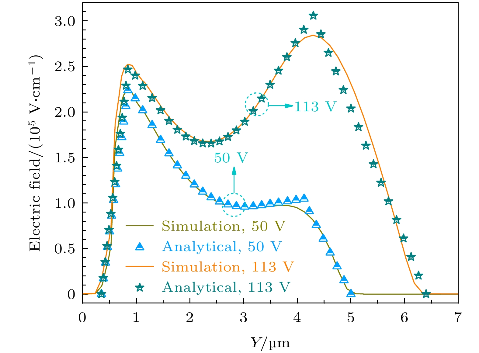
图 9 不同电压下电场解析结果和仿真结果的对比
Figure 9. Comparison of electric field analysis results and simulation results under different drain-source voltages.
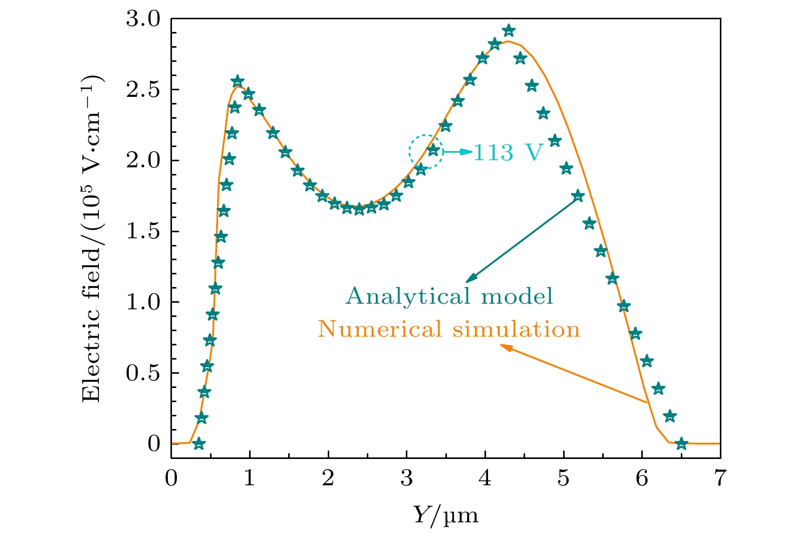
图 10 修正后的电场解析模型
Figure 10. Revised electric field analytical model.
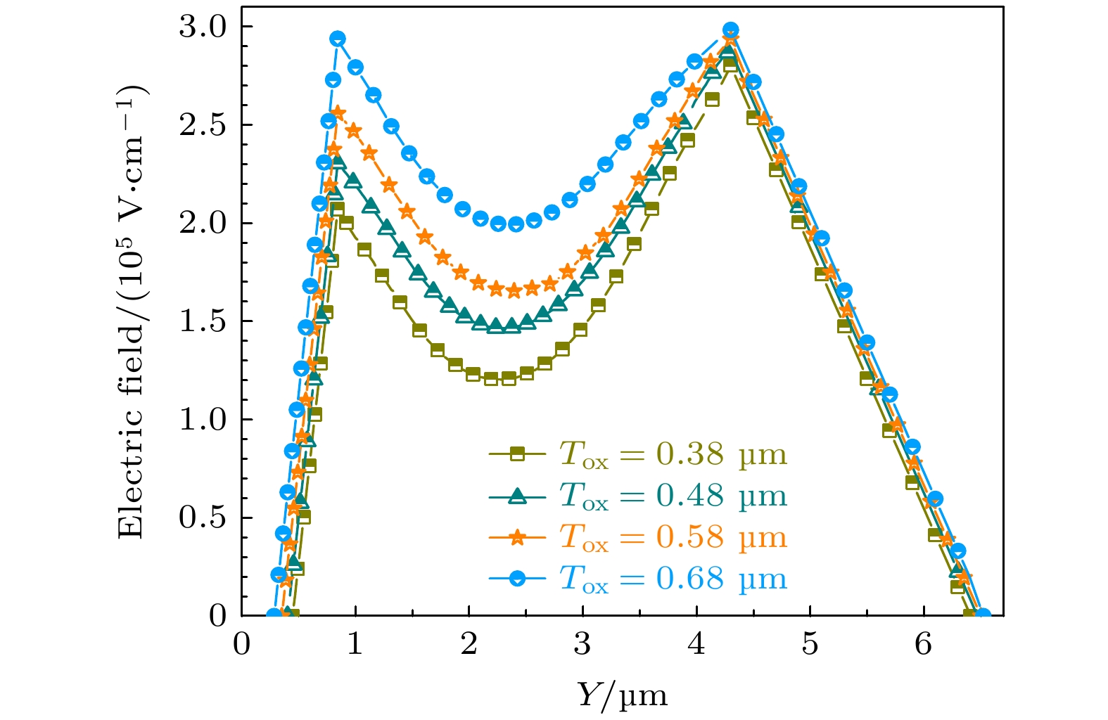
图 11 不同场氧厚度下的电场解析模型
Figure 11. Analytical model of electric field under different field oxygen thicknesses.
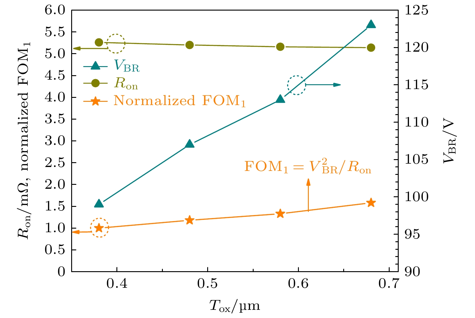
图 12 不同场氧厚度下的Ron、VBR、归一化优值FOM1
Figure 12. Ron, VBR, and normalized FOM1 under different
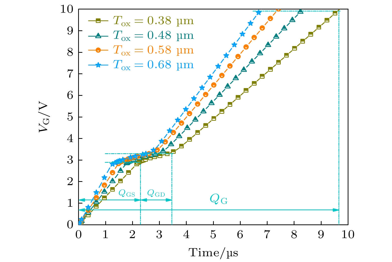
图 13 不同场氧厚度下的栅电荷
Figure 13. Gate charges under different field oxygen thicknesses.

图 14 不同场氧厚度下的Ron、Qg、优值FOM2
Figure 14. Ron, Qg, and FOM2 under different field oxygen thickness.
表 1 SGT-MOSFE产品具体结构参数
Table 1. The structural parameters of SGT-MOSFET product.
参数 掺杂浓度/cm–3 厚度/宽度(µm/µm) n+源区 5.0×10¹⁹ 0.30 p体区 1.3×10¹⁷ 0.80 p漂移区 1.5×10¹⁶ 7.40 p+衬底 1.5×10¹⁹ 15.00 沟槽深度① — 4.70 屏蔽栅深度② — 4.30 控制栅深度③ — 1.00 单元胞宽度④ — 3.20 沟槽宽度⑤ — 1.80 台面宽度⑥ — 1.40 场氧厚度⑦ — 0.58  DownLoad: CSV
表 2 表达式中的具体参数值
Table 2. Specific parameter values in expressions.
参数 参数值 单位 ND 1.5×1016 cm–3 NA 4×1016 cm–3 q 1.602×10⁻¹⁹ C ${\varepsilon }_{ {\rm{s} }{\rm{i} } }$ 1.053626×10⁻¹² F/cm $ {D}_{{\rm{p}}} $ 0.8×10⁻⁴ cm Ln 3.5×10⁻⁴ cm Wn 0.70×10⁻⁴ cm Tox 0.58×10⁻⁴ cm K 3.0512820513 — T 1.2005×10⁻⁴ cm t 0.49497×10⁻⁴ cm
DownLoad: CSV
-
[1] Nguyen M H, Kwak S 2020 Electronics 9 2068
Google Scholar
[2] Huang A Q 2017 P. IEEE. 105 2019
Google Scholar
[3] Krishnan R 2020 IEEE Ind. Electron. Mag. 16 105
[4] Williams R K, Darwish M N, Blanchard R A, Siemieniec R, Rutter P, Kawaguchi Y 2017 IEEE. T. Electron. Dev. 64 692
Google Scholar
[5] Xi J, Wang J, Lu J, Chen J, Xin Y, Li Z, Tu C, Shen Z J 2018 Microelectron. Reliab. 88–90 593
[6] Park C, Havanur S, Shibib A, Terrill K 2016 Proceedings of the 28th International Symposium on Power Semiconductor Devices and ICs Prague, Czech Republic, June 12–16, 2016 p387
[7] Wang Y, Hu H F, Jiao W 2012 IEEE. T. Electron. Dev. 59 3037
Google Scholar
[8] Tian Y, Yang Z, Xu Z, Liu S, Sun W F, Shi L, Zhu Y, Ye P, Zhou J 2018 Superlattice. Microst. 116 151
Google Scholar
[9] Su L, Wang C L, Yang W H, An J 2022 Microelectron. Reliab. 139 114822
Google Scholar
[10] Tong C F, Mawby P A, Covington J A 2009 13th European Conference on Power Electronics and Applications Barcelona, Spain, September 8–10, 2009 10939294
[11] Wang Y, Yu C H, Hu H F, Dou Z 2013 IET. Power. Electron. 7 2964
[12] Wang Y, Lan H, Dou Z, Hu H F 2014 IET. Power. Electron. 7 2030
Google Scholar
[13] Deng S, Hossain Z, Taniguchi T 2017 IEEE. T. Electron. Dev. 64 735
Google Scholar
[14] Wang W, Ning R, Shen Z J 2017 IEEE. Electr. Device. L. 38 1055
Google Scholar
[15] Chien F T, Wang Z Z, Lin C L, Kang T K, Chen C W, Chiu H C 2020 Micromachines 11 504
Google Scholar
[16] Chen R, Wang L, Jiu N, Zhang H, Guo, M 2020 Electronics 9 745
Google Scholar
[17] Wang Z K, Qiao M, Fang D, Wang R D, Qi Z, Li Z J, Zhang B 2020 IEEE. Electr. Device. L. 41 749
Google Scholar
[18] Su L, Wang C L, Yang W H, Zhang C 2023 Microelectron. Reliab. 143 114950
Google Scholar
[19] Zhang W T, Pu S, Lai C L, Ye L, Cheng S, Zhang S, He B, Wang Z, Luo X, Qiao M 2018 Proceedings of the 30th International Symposium on Power Semiconductor Devices and ICs Chicago, IL, USA, May 13–17, 2018 p475
[20] Zhang W T, Ye L, Fang D, Qiao M, Xiao K, He B Y, Li Z J, Zhang B 2019 IEEE. T. Electron. Dev. 66 1416
Google Scholar
[21] Zhang W T, Zhang B, Qiao M, Wu L J, Mao K, Li Z J 2014 IEEE. T. Electron. Dev. 61 518
Google Scholar
[22] Oetjen J, Jungblut R, Kuhlmann U, Arkenau J, Sittig R 2000 Solid. State. Electronic. 44 117
Google Scholar
[23] Jacoboni C, Canali C, Ottaviani G, Quaranta A A 1977 Solid. State. Electronic. 20 77
Google Scholar

 DownLoad:
Catalog
Metrics
- Abstract views: 2767
- PDF Downloads: 138
- Cited By: 0
