


-
With the extensive integration of portable computers and smartphones with “Internet of Things” technology, further miniaturization, high reading/writing speed and big storage capacity are required for the new-generation non-volatile memory devices. Compared with traditional charge memory and magnetoresistive memory, resistive random access memory (RRAM) based on transition metal oxides is one of the promising candidates due to its low power consumption, small footprint, high stack ability, fast switching speed and multi-level storage capacity. Inspired by the excellent resistive switching characteristics of NiO and HfO2, NiOx films are deposited by magnetron sputtering on the Pt $\langle111\rangle $ layer and the polycrystalline HfO2 film, respectively. Their microstructures, resistive switching characteristics and conductive mechanisms are studied. X-ray diffractometer data show the$\langle111\rangle $ preferred orientation for the NiOx film deposited on the Pt$\langle111\rangle $ layer but the$\langle100\rangle $ preferred one for the film deposited on the polycrystalline HfO2 layer. X-ray photoelectron depth profile of Ni 2p core level reveals that the NiOx film is the mixture of oxygen-deficient NiO and Ni2O3. NiOx(111) films show bipolar resistive switching (RS) characteristics with a clockwise current-voltage (I-V) loop, but its ratio of the high resistance to the low resistance (RH/RL) is only ~10, and its endurance is also poor. The NiOx(200)/HfO2 stack exhibits bipolar RS characteristics with a counterclockwise I-V loop. The RH/RL is greater than 104, the endurance is about 104 cycles, and the retention time exceeds 104 s. In the initial stage, the HfO2/NiOx(200)/HfO2 stack shows similar bi-level RS characteristics to the NiOx(200)/HfO2 stack. However, in the middle and the last stages, its I-V curves gradually evolve into tri-level RS characteristics with a “two-step Setting process” in the positive voltage region, showing potential applications in multilevel nonvolatile memory devices and brain-like neural synapses. Its I-V curves in the high and the low resistance state follow the relationship of ohmic conduction ($ I \propto V $ ), while the I-V curves in the intermediate resistance state are dominated by the space-charge-limited-current mechanism ($ I \propto V^2 $ ). The tri-level RS phenomena are attributed to the coexistence of the oxygen-vacancy conductive filaments in the NiOx(200) film and the space charge limited current in the upper HfO2 film.[1] Lanza M, Sebastian A, Lu W D, Le Gallo M, Chang M F, Akinwande D, Puglisi F M, Alshareef H N, Liu M, Roldan J B 2022 Science 376 1066
 Google Scholar
[2] Zhou G D, Ji X Y, Li J, Zhou F C, Dong Z K, Yan B T, Sun B, Wang W H, Hu X F, Song Q L, Wang L D, Duan S K 2022 iScience 25 105240
Google Scholar
[3] Zhou G D, Sun B, Hu X F, Sun L F, Zou Z, Xiao B, Qiu W K, Wu B, Li J, Han J J, Liao L P, Xu C Y, Xiao G, Xiao L H, Cheng J B, Zheng S H, Wang L D, Song Q L, Duan S K 2021 Adv. Sci. 8 2003765
Google Scholar
[4] 朱玮, 郭恬恬, 刘兰, 周荣荣 2021 物理学报 70 068502
Google Scholar
Zhu W, Guo T T, Liu L, Zhou R R 2021 Acta Phys. Sin. 70 068502
Google Scholar
[5] Gibbons J F, Beadle W E 1964 Solid-State Electron. 7 785
Google Scholar
[6] Wang G Y, Hu L, Xia Y D, Li Q, Xu Q Y 2020 J. Magn. Magn. Mater. 493 165728
Google Scholar
[7] Xia W Y, Sun X W, Yin Y F, Jia C H, Li G Q, Zhang W F 2020 AIP Adv. 10 105319
Google Scholar
[8] Chu J X, Li Y, Fan X H, Shao H H, Duan W J, Pei Y L 2018 Semicond. Sci. Technol. 33 115007
Google Scholar
[9] Jung K, Choi J, Kim Y, Im H, Seo S, Jung R, Kim D, Kim J S, Park B H, Hong J P 2008 J. Appl. Phys. 103 034504
Google Scholar
[10] Yuan X C, Wei X H, Dai B, Zeng H Z 2016 Appl. Surf. Sci. 362 506
Google Scholar
[11] D'Aquila K, Liu Y Z, Iddir H, Petford-Long A K 2015 Phys. Status Solidi RRL 9 301
Google Scholar
[12] Lee S, Kim D, Eom H, Kim W B, Yoo B 2014 Jpn. J. Appl. Phys. 53 024202
Google Scholar
[13] Ge N N, Gong C H, Yuan X C, Zeng H Z, Wei X H 2018 RSC Adv. 8 29499
Google Scholar
[14] Li J C, Hou X Y, Cao Q 2014 J. Appl. Phys. 115 164507
Google Scholar
[15] Kim J, Na H, Lee S, Sung Y H, Yoo J H, Lee D S, Ko D H, Sohn H 2011 Curr. Appl. Phys. 11 e70
Google Scholar
[16] Kim J, Lee K, Sohn H 2009 J. Electrochem. Soc. 156 H881
Google Scholar
[17] Ma G K, Tang X L, Zhang H W, Zhong Z Y, Li X, Li J, Su H 2017 J. Mater. Sci. 52 238
Google Scholar
[18] Huang Y C, Chen P Y, Chin T S, Liu R S, Huang C Y, Lai C H 2012 Appl. Phys. Lett. 101 153106
Google Scholar
[19] Kim D C, Lee M J, Ahn S E, Seo S, Park J C, Yoo I K, Beak I G, Kim H J, Yim E K, Lee J E, Park S O, Kim H S, Chung U I, Moon J T, Ryu B I 2006 Appl. Phys. Lett. 88 232106
Google Scholar
[20] Qiu X Y, Wang R X, Zhang Z, Wei M L, Ji H, Chai Y, Zhou F C, Dai J Y, Zhang T, Li L T, Meng X S 2017 Appl. Phys. Lett. 111 142103
Google Scholar
[21] Chen X M, Zhou H, Wu G H, Bao D H 2011 Appl. Phys. A-Mater. Sci. Process. 104 477
Google Scholar
[22] Li S, Wei X H, Lei Y, Yuan X C, Zeng H Z 2016 Appl. Surf. Sci. 389 977
Google Scholar
[23] Zhang T, Zhang Z, Chan C H, Li L T, Wei M L, Meng X S, Dai J Y, Qiu X Y 2018 J. Phys. D: Appl. Phys. 51 305105
Google Scholar
[24] Banerjee W, Kashir A, Kamba S 2022 Small 18 2107575
Google Scholar
[25] Park M, Jeon B, Park J, Kim S 2022 Nanomaterials 12 4206
Google Scholar
[26] Chen Y J, Chang K C, Chang T C, Chen H L, Young T F, Tsai T M, Zhang R, Chu T J, Ciou J F, Lou J C, Chen K H, Chen J H, Zheng J C, Sze S M 2014 IEEE Electron Device Lett. 35 1016
Google Scholar
[27] Yan X Y, Wang X T, Wang D, et al. 2020 Nanotechnology 31 115209
Google Scholar
[28] Yin Y X, Xie Y S, Chen T, Xiang Y J, Zhou K, Qiu X Y 2023 Appl. Surf. Sci. 613 155994
Google Scholar
[29] Qiu X Y, Wang R X, Li G Q, et al. 2017 Appl. Surf. Sci. 406 212
Google Scholar
[30] Kim K S, Winograd N 1974 Surf. Sci. 43 625
Google Scholar
[31] Khan M Q, Ahmad K, Alsalme A, Kim H 2022 Mater. Chem. Phys. 289 126463
Google Scholar
[32] Smolarek M, Kierzkowska-Pawlak H, Kapica R, Fronczak M, Sitarz M, Lesniak M, Tyczkowski J 2021 Catalysts 11 905
Google Scholar
[33] Luo J M, Zhang H N, Chen S H, Yang X D, Bu S L, Wen J P 2016 Chem. Phys. Lett. 652 98
Google Scholar
[34] 潘峰, 陈超 2014 阻变存储器材料与器件 (北京: 科学出版社) 第43页
Pan F, Chen C 2014 Resistive Random Access Memory Materials and Devices (Beijing: Science Press) p43 (in Chinese)
[35] Sze S M, Ng K K 2007 Physics of Semiconductor Devices (3rd Ed.) (America: John Wiley & Sons, Inc.) p227
[36] Siddik A, Halder P K, Garu P, et al. 2020 J. Phys. D: Appl. Phys. 53 295103
Google Scholar
[37] Li Y, Fang P W, Fan X H, Pei Y L 2020 Semicond. Sci. Technol. 35 055004
Google Scholar
[38] Zhang W, Lei J Z, Dai Y X, Zhang X H, Kang L M, Peng B W, Hu F R 2022 Nanotechnology 33 255703
Google Scholar
[39] Li Z H, Li J C, Cui H P 2021 J. Alloys Compd. 858 158091
Google Scholar
[40] Ismail M, Chand U, Mahata C, Nebhen J, Kim S 2022 J. Mater. Sci. Technol. 96 94
Google Scholar
[41] Wang W, Covi E, Lin Y H, et al. 2021 IEEE Trans. Electron Devices 68 4342
Google Scholar
[42] Hong D S, Wang W X, Chen Y S, Sun J R, Shen B G 2014 Appl. Phys. Lett. 105 113504
Google Scholar
[43] Yuan F, Shen S S, Zhang Z G, Pan L Y, Xu J 2016 Superlattices Microstruct. 91 90
Google Scholar
[44] Razi P M, Angappane S, Gangineni R B 2021 Mater. Sci. Eng. B-Adv. 263 114852
Google Scholar
[45] Sun B, Zhang X J, Zhou G D, Yu T, Mao S S, Zhu S H, Zhao Y, Xia Y D 2018 J. Colloid Interface Sci. 520 19
Google Scholar
-
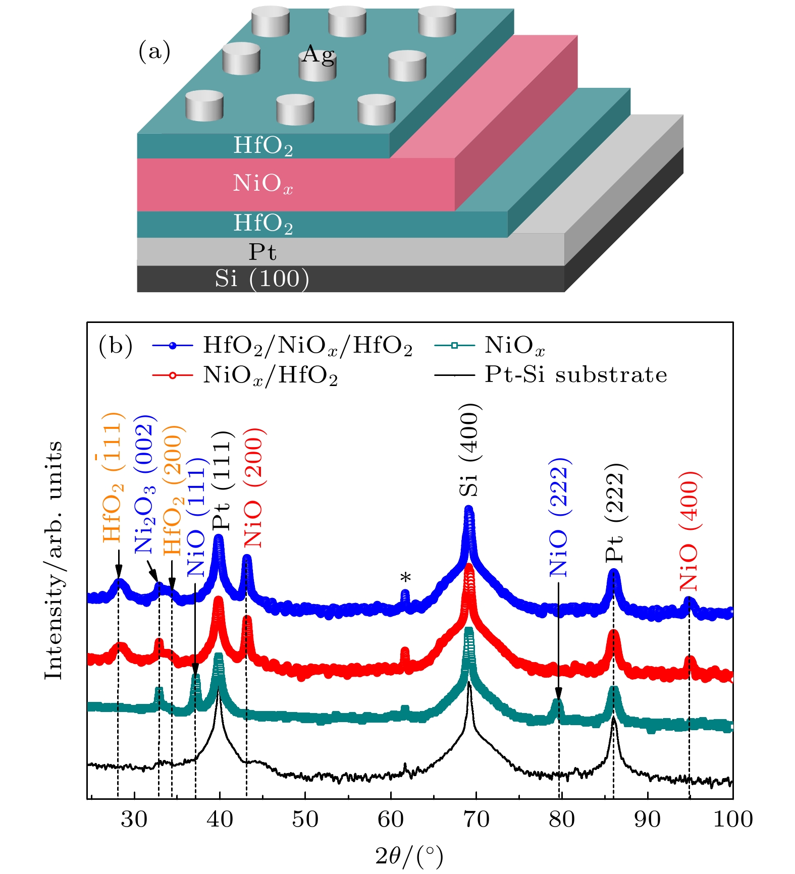
图 1 (a) Ag/HfO2/NiOx/HfO2/Pt-Si堆栈器件结构示意图; (b) 沉积在Pt-Si衬底上的NiOx薄膜, NiOx/HfO2和HfO2/NiOx/HfO2堆栈样品的XRD谱
Figure 1. (a) Schematic diagram of the Ag/HfO2/NiOx/HfO2/Pt-Si stack; (b) XRD spectra of the NiOx film, NiOx/HfO2 and HfO2/NiOx/HfO2 stacks on Pt coated Si (Pt-Si) substrates.
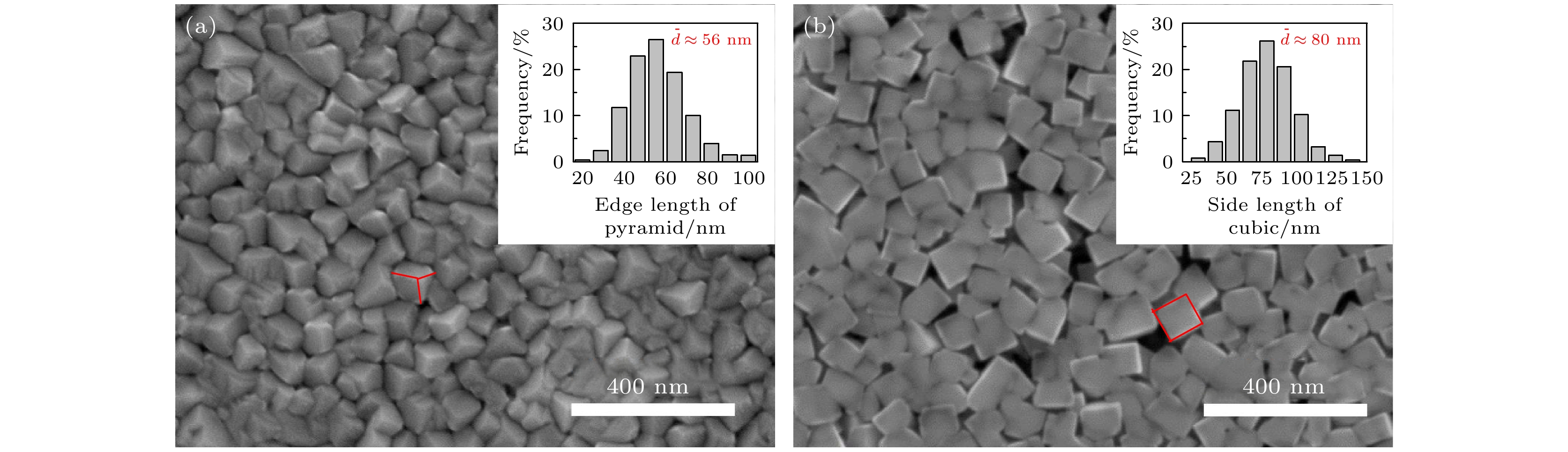
图 2 择优取向的(a) NiOx
$\langle111\rangle $ 和(b) NiOx$\langle100\rangle $ 薄膜SEM照片和粒径分布统计图(右上插图)Figure 2. Top-view SEM images and particle size distributions (upper-right insets) of NiOx films with the preferred (a)
$\langle111\rangle $ and (b)$\langle100\rangle $ orientations, respectively.
图 3 HfO2/NiOx/HfO2堆栈样品横截面的(a) SEM照片, (b) EDS面扫描总谱以及(c) Ni, (d) O, (e) Pt和(f) Si元素的面分布图. 图(b)中插图为Ni, O, Pt和Hf元素的原子百分含量柱状图
Figure 3. (a) Cross-sectional SEM image, (b) EDS spectrum, and EDS maps of (c) Ni, (d) O, (e) Pt and (f) Si elements for the HfO2/NiOx/HfO2 stack on the Pt-Si substrate. Inset in Fig.(b) shows the atomic percent of Ni, O, Pt, and Hf elements in the sample.

图 4 (a) 沉积在Pt-Si衬底上的HfO2/NiOx/HfO2堆栈横截面的HRTEM照片; 图(a)中的(b) HfO2/NiOx界面局部区域(红色方框标注)和(c) NiOx/HfO2/Pt局部区域(白色方框标注)的高倍数HRTEM照片
Figure 4. (a) HRTEM images for the cross sectional HfO2/NiOx/HfO2 stack on Pt-Si substrate. Magnified HRTEM images for (b) the HfO2/NiOx and (c) the NiOx/HfO2/Pt interfaces marked with the red and the white boxes in Fig.(a), respectively.

图 5 HfO2/NiOx/HfO2堆栈中Hf, Ni, Pt和O的原子百分含量随刻蚀次数的变化
Figure 5. Variations of the atomic percent for Hf, Ni, Pt, and O in the HfO2/NiOx/HfO2 stack with etching times.
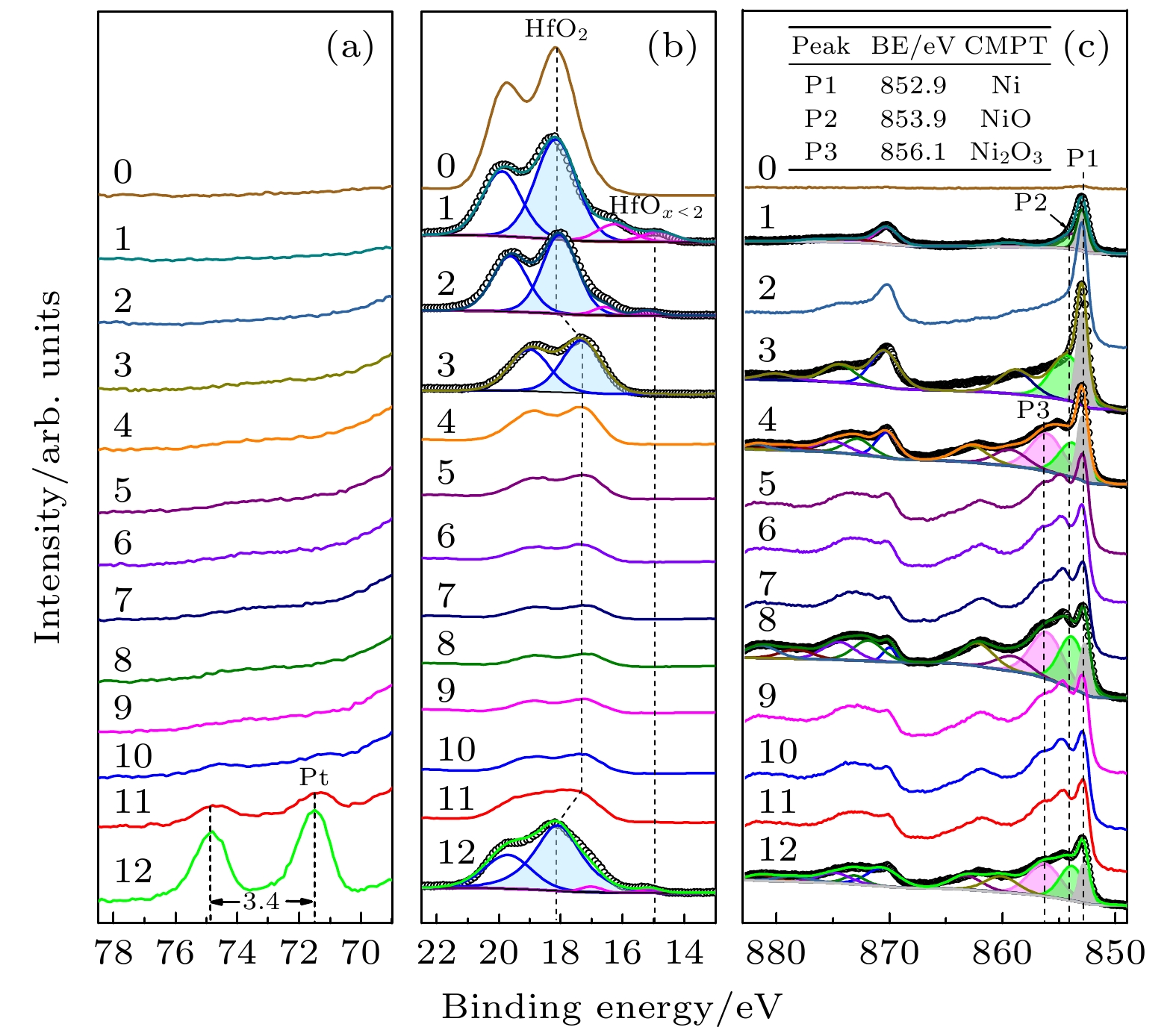
图 6 HfO2/NiOx/HfO2堆栈样品的(a) Pt 4f, (b) Hf 4f和(c) Ni 2p核心能级的XPS深度剖析谱
Figure 6. XPS depth profiles of (a) Pt 4f, (b) Hf 4f and (c) Ni 2p core levels for the HfO2/NiOx/HfO2 stack.

图 7 P1, P2和P3峰面积百分比随刻蚀次数的变化
Figure 7. Variations of the peak area percentage for P1, P2, and P3 sub-peaks with etching times.
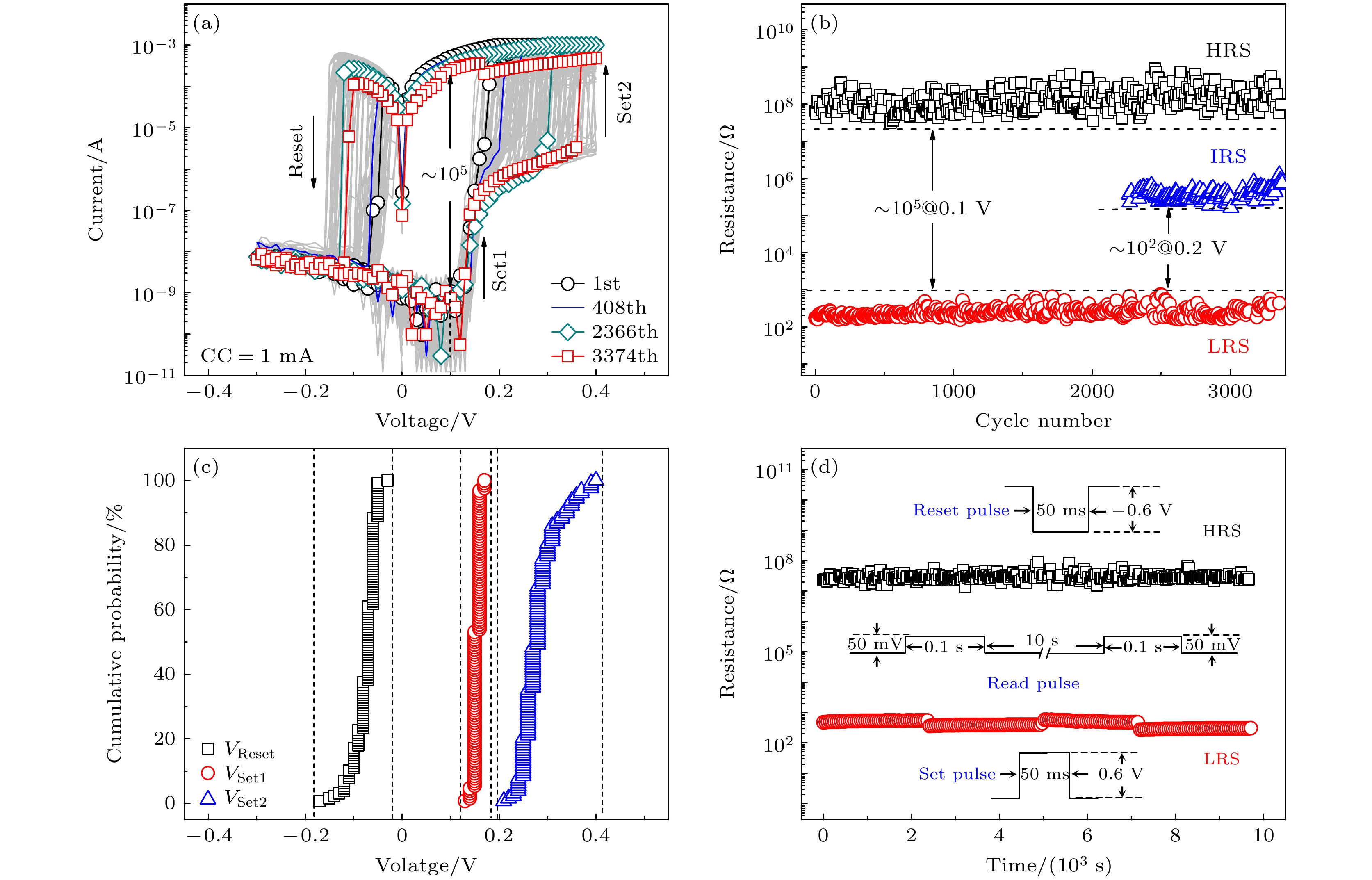
图 8 HfO2/NiOx/HfO2堆栈器件的电阻开关特性 (a) I-V回线; (b) 0.1 V电压读取的高电阻态, 中间电阻态和低电阻态阻值随循环周期数的变化; (c) VSet1, VSet2和VReset的累积概率分布以及(d) 器件在高(低)电阻态的持续时间
Figure 8. Resistive switching properties of the HfO2/NiOx/HfO2 stack: (a) I-V loops; (b) variations of resistance for the HRS, IRS and LRS with the cycle number at the reading voltage of 0.1 V; (c) cumulative probability distributions of VSet1, VSet2 and VReset; (d) retention time of the HRS and the LRS.
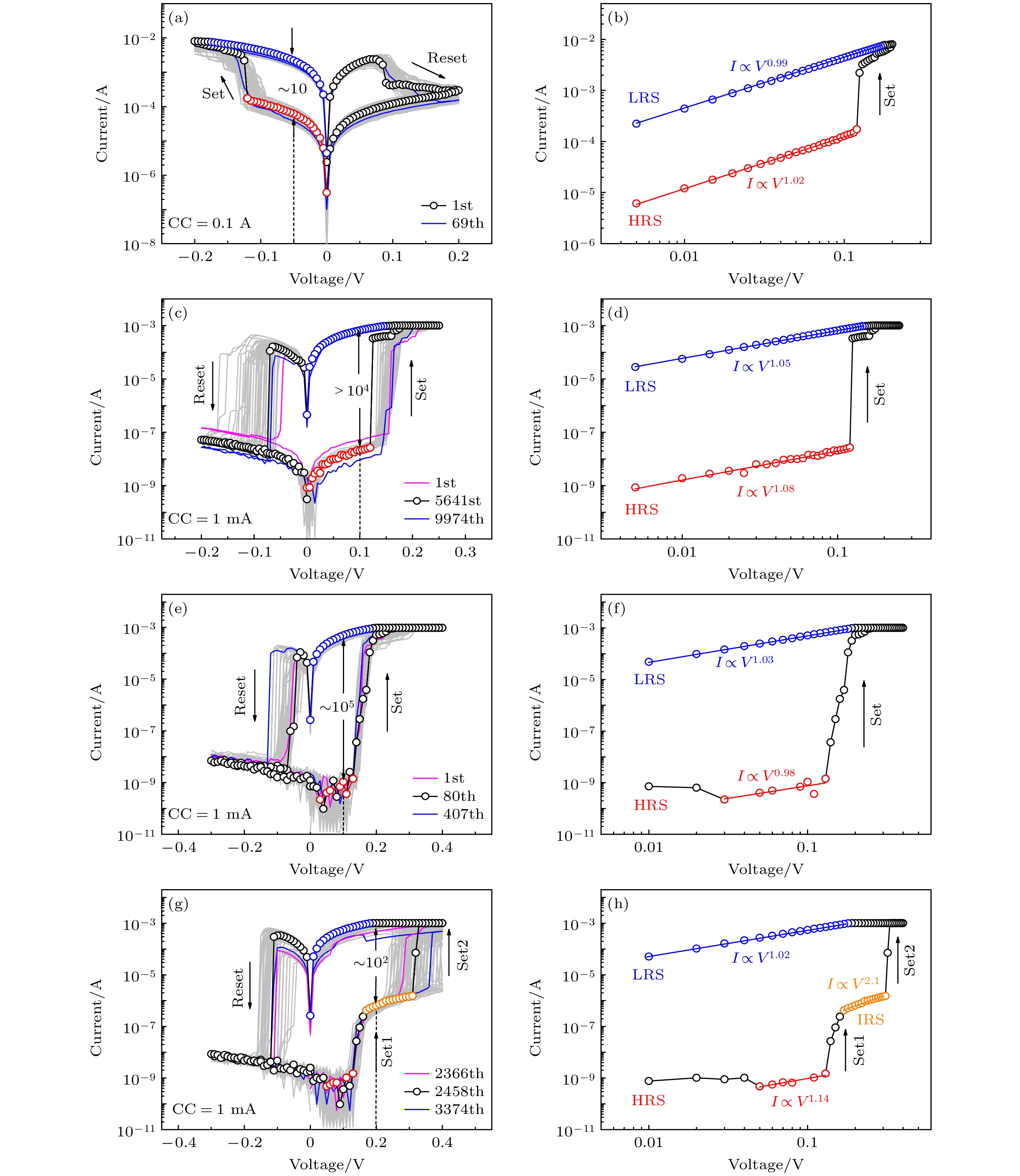
图 9 (a), (b) NiOx薄膜, (c), (d) NiOx/HfO2和(e)—(h) HfO2/NiOx/HfO2堆栈在对数-线性坐标中的I-V回线及其在双对数坐标中绘制的Set过程附近的I-V曲线
Figure 9. I-V loops in logarithmic-linear scale and replotted I-V curves in double-logarithmic scale near the Set process of RRAM cells based on (a), (b) NiOx films, (c), (d) NiOx/HfO2 and (e)–(h) HfO2/NiOx/HfO2 stacks, respectively.

图 10 HfO2/NiOx/HfO2堆栈器件电阻开关微观机制示意图 (a) 扩散过程; (b) Set1过程; (c) Set2过程; (d) Reset过程
Figure 10. Schematic illustrations of the resistive switching mechanism for the HfO2/NiOx/HfO2 stack in the (a) diffusion; (b) Set1; (c) Set2 and (d) Reset processes
表 1 Ag/HfO2/NiOx/HfO2/Pt堆栈器件的制备工艺参数
Table 1. Preparation parameters of the Ag/HfO2/NiOx/HfO2/Pt stack.
成分 溅射源
(99.99%纯度)生长气氛
流量(比)衬底
温度/℃溅射方式
功率/W, 偏压/V生长
时间/min退火气氛
流量(比)退火
温度/℃退火
时间/minPt金属层 Pt金属靶 2.7 Pa Ar+O2
Ar∶O2 = 17∶3700 直流
25, 05 — — — HfO2薄膜 HfO2陶瓷靶 3 Pa Ar
30 sccm350 射频
70, 020 3 Pa O2
30 sccm350 30 NiOx薄膜 Ni金属靶 0.5 Pa Ar+O2
Ar∶O2 = 4∶1700 射频
60, 090 0.5 Pa Ar+O2
Ar∶O2 = 4∶1700 30 Ag电极 Ag金属靶 0.5 Pa Ar
30 sccm250 直流
25, –10010 — — — 注: sccm为cm3/min.  DownLoad: CSV
表 2 各种氧化物/NiOx堆栈RRAM器件的电阻开关性能参数
Table 2. Resistive switching parameters of RRAM cells based on various oxide/NiOx stacks.
Cell structure Switching type VSet/V VReset/V RH/RL Endurance Retention/s Ref. NiFe/Al2O3/NiO/Pt Unipolar 2.30—4.20 0.55—1.50 ~1×10³ >1×10² 1×10⁴ [6] Pt/IrO2/NiO/IrO2/Pt Unipolar 1.43 0.41 > 1×10² 2×10² — [19] Ag/HfO2/NiO/Pt Bipolar 0.20 –0.20 > 1×10³ > 5×10³ > 1×10³ [20] Pt/NiO/Mg0.6Zn0.4O/Pt Rectifying — 0.54—0.62 ~1×10⁶ 1×10² 6×10⁴ [21] Au/BaTiO3/NiO/Pt Unipolar 2.00 1.00 — — — [22] Ag/HfO2/nb-NiO/Pt Bipolar 0.16—0.38 –0.19— –0.38 ~1×10⁴ 1.2×10³ >1×10⁴ [28] Pt/BiFeO3/NiO/Pt Bipolar 1.00—1.50 –0.20— –0.60 > 10 30 — [33] Ag/NiOx/HfO2/Pt Bipolar 0.12—0.18 –0.02— –0.17 > 1×10⁴ ~1×10⁴ > 1×10⁴ Reference cell Ag/HfO2/NiOx/HfO2/Pt Bipolar Set1: 0.13—0.17 –0.03— –0.17 ~1×10⁵ > 3×10³ ~1×10⁴ This work Set2: 0.21—0.40 ~1×10²
DownLoad: CSV
-
[1] Lanza M, Sebastian A, Lu W D, Le Gallo M, Chang M F, Akinwande D, Puglisi F M, Alshareef H N, Liu M, Roldan J B 2022 Science 376 1066
Google Scholar
[2] Zhou G D, Ji X Y, Li J, Zhou F C, Dong Z K, Yan B T, Sun B, Wang W H, Hu X F, Song Q L, Wang L D, Duan S K 2022 iScience 25 105240
Google Scholar
[3] Zhou G D, Sun B, Hu X F, Sun L F, Zou Z, Xiao B, Qiu W K, Wu B, Li J, Han J J, Liao L P, Xu C Y, Xiao G, Xiao L H, Cheng J B, Zheng S H, Wang L D, Song Q L, Duan S K 2021 Adv. Sci. 8 2003765
Google Scholar
[4] 朱玮, 郭恬恬, 刘兰, 周荣荣 2021 物理学报 70 068502
Google Scholar
Zhu W, Guo T T, Liu L, Zhou R R 2021 Acta Phys. Sin. 70 068502
Google Scholar
[5] Gibbons J F, Beadle W E 1964 Solid-State Electron. 7 785
Google Scholar
[6] Wang G Y, Hu L, Xia Y D, Li Q, Xu Q Y 2020 J. Magn. Magn. Mater. 493 165728
Google Scholar
[7] Xia W Y, Sun X W, Yin Y F, Jia C H, Li G Q, Zhang W F 2020 AIP Adv. 10 105319
Google Scholar
[8] Chu J X, Li Y, Fan X H, Shao H H, Duan W J, Pei Y L 2018 Semicond. Sci. Technol. 33 115007
Google Scholar
[9] Jung K, Choi J, Kim Y, Im H, Seo S, Jung R, Kim D, Kim J S, Park B H, Hong J P 2008 J. Appl. Phys. 103 034504
Google Scholar
[10] Yuan X C, Wei X H, Dai B, Zeng H Z 2016 Appl. Surf. Sci. 362 506
Google Scholar
[11] D'Aquila K, Liu Y Z, Iddir H, Petford-Long A K 2015 Phys. Status Solidi RRL 9 301
Google Scholar
[12] Lee S, Kim D, Eom H, Kim W B, Yoo B 2014 Jpn. J. Appl. Phys. 53 024202
Google Scholar
[13] Ge N N, Gong C H, Yuan X C, Zeng H Z, Wei X H 2018 RSC Adv. 8 29499
Google Scholar
[14] Li J C, Hou X Y, Cao Q 2014 J. Appl. Phys. 115 164507
Google Scholar
[15] Kim J, Na H, Lee S, Sung Y H, Yoo J H, Lee D S, Ko D H, Sohn H 2011 Curr. Appl. Phys. 11 e70
Google Scholar
[16] Kim J, Lee K, Sohn H 2009 J. Electrochem. Soc. 156 H881
Google Scholar
[17] Ma G K, Tang X L, Zhang H W, Zhong Z Y, Li X, Li J, Su H 2017 J. Mater. Sci. 52 238
Google Scholar
[18] Huang Y C, Chen P Y, Chin T S, Liu R S, Huang C Y, Lai C H 2012 Appl. Phys. Lett. 101 153106
Google Scholar
[19] Kim D C, Lee M J, Ahn S E, Seo S, Park J C, Yoo I K, Beak I G, Kim H J, Yim E K, Lee J E, Park S O, Kim H S, Chung U I, Moon J T, Ryu B I 2006 Appl. Phys. Lett. 88 232106
Google Scholar
[20] Qiu X Y, Wang R X, Zhang Z, Wei M L, Ji H, Chai Y, Zhou F C, Dai J Y, Zhang T, Li L T, Meng X S 2017 Appl. Phys. Lett. 111 142103
Google Scholar
[21] Chen X M, Zhou H, Wu G H, Bao D H 2011 Appl. Phys. A-Mater. Sci. Process. 104 477
Google Scholar
[22] Li S, Wei X H, Lei Y, Yuan X C, Zeng H Z 2016 Appl. Surf. Sci. 389 977
Google Scholar
[23] Zhang T, Zhang Z, Chan C H, Li L T, Wei M L, Meng X S, Dai J Y, Qiu X Y 2018 J. Phys. D: Appl. Phys. 51 305105
Google Scholar
[24] Banerjee W, Kashir A, Kamba S 2022 Small 18 2107575
Google Scholar
[25] Park M, Jeon B, Park J, Kim S 2022 Nanomaterials 12 4206
Google Scholar
[26] Chen Y J, Chang K C, Chang T C, Chen H L, Young T F, Tsai T M, Zhang R, Chu T J, Ciou J F, Lou J C, Chen K H, Chen J H, Zheng J C, Sze S M 2014 IEEE Electron Device Lett. 35 1016
Google Scholar
[27] Yan X Y, Wang X T, Wang D, et al. 2020 Nanotechnology 31 115209
Google Scholar
[28] Yin Y X, Xie Y S, Chen T, Xiang Y J, Zhou K, Qiu X Y 2023 Appl. Surf. Sci. 613 155994
Google Scholar
[29] Qiu X Y, Wang R X, Li G Q, et al. 2017 Appl. Surf. Sci. 406 212
Google Scholar
[30] Kim K S, Winograd N 1974 Surf. Sci. 43 625
Google Scholar
[31] Khan M Q, Ahmad K, Alsalme A, Kim H 2022 Mater. Chem. Phys. 289 126463
Google Scholar
[32] Smolarek M, Kierzkowska-Pawlak H, Kapica R, Fronczak M, Sitarz M, Lesniak M, Tyczkowski J 2021 Catalysts 11 905
Google Scholar
[33] Luo J M, Zhang H N, Chen S H, Yang X D, Bu S L, Wen J P 2016 Chem. Phys. Lett. 652 98
Google Scholar
[34] 潘峰, 陈超 2014 阻变存储器材料与器件 (北京: 科学出版社) 第43页
Pan F, Chen C 2014 Resistive Random Access Memory Materials and Devices (Beijing: Science Press) p43 (in Chinese)
[35] Sze S M, Ng K K 2007 Physics of Semiconductor Devices (3rd Ed.) (America: John Wiley & Sons, Inc.) p227
[36] Siddik A, Halder P K, Garu P, et al. 2020 J. Phys. D: Appl. Phys. 53 295103
Google Scholar
[37] Li Y, Fang P W, Fan X H, Pei Y L 2020 Semicond. Sci. Technol. 35 055004
Google Scholar
[38] Zhang W, Lei J Z, Dai Y X, Zhang X H, Kang L M, Peng B W, Hu F R 2022 Nanotechnology 33 255703
Google Scholar
[39] Li Z H, Li J C, Cui H P 2021 J. Alloys Compd. 858 158091
Google Scholar
[40] Ismail M, Chand U, Mahata C, Nebhen J, Kim S 2022 J. Mater. Sci. Technol. 96 94
Google Scholar
[41] Wang W, Covi E, Lin Y H, et al. 2021 IEEE Trans. Electron Devices 68 4342
Google Scholar
[42] Hong D S, Wang W X, Chen Y S, Sun J R, Shen B G 2014 Appl. Phys. Lett. 105 113504
Google Scholar
[43] Yuan F, Shen S S, Zhang Z G, Pan L Y, Xu J 2016 Superlattices Microstruct. 91 90
Google Scholar
[44] Razi P M, Angappane S, Gangineni R B 2021 Mater. Sci. Eng. B-Adv. 263 114852
Google Scholar
[45] Sun B, Zhang X J, Zhou G D, Yu T, Mao S S, Zhu S H, Zhao Y, Xia Y D 2018 J. Colloid Interface Sci. 520 19
Google Scholar


 DownLoad:


Catalog
Metrics
- Abstract views: 1764
- PDF Downloads: 30
- Cited By: 0
