


-
Na2KSb photocathodes have many applications in vacuum optoelectronic devices, such as photomultiplier tubes, image intensifiers, and streak image tubes for high-speed detection and imaging in extremely weak light environments, due to their advantages of high temperature resistance, small dark current, low vacuum requirement, low fabrication cost and high fabrication flexibility. In addition, this type of photocathode has important application prospect in high brightness accelerator photoinjectors. To guide the fabrication of high-sensitivity Na2KSb photocathodes, Na2KSb surfaces with different surface orientations and atom terminations are investigated by the first-principles calculation method based on the density functional theory to obtain the most stable and most favorable surface for electron emission. From the perspectives of surface energy, adsorption energy, and work function before and after Cs adsorption, it is revealed that the Na2KSb (111) K surface exhibits superior surface stability and electron emission capability. Furthermore, the electronic structure and optical properties of Cs adsorption and Cs/O co-adsorption on the Na2KSb (111) K surface under different Cs coverages are analyzed, and the mechanism of Cs/O deposition on Na2KSb surface is studied. The adsorption energy of Cs in the Cs/O adsorption model is much larger than that in the single Cs adsorption model, indicating that the adsorption of O atoms on the Na2KSb surface can make the adsorption of Cs atoms on the surface stronger, and thus increasing the adhesion of Cs atoms on the surface. After adsorption of Cs on the Na2KSb (111)K surface, the surface work function only decreases by 0.02 eV, while the maximum work function decrease for the Cs/O adsorbed surface is 0.16 eV, with the Cs coverage of 2/4 ML and the O coverage of 1/4 ML. The adsorption of Cs/O atoms on the surface facilitates the charge transfer above the surface and results in charge accumulation, which can form the effective surface dipole moment. The magnitude of the surface dipole moment is directly related to the change of work function. Furthermore, through the analysis of the electronic band structure and density of states, it is found that the adsorbed Cs atoms have additional contribution to the band structure near the conduction band minimum. After the introduction of O atoms, the valence band moves up, also the bottom of the conduction band and the top of the valence band become flat. The Cs/O deposition is beneficial to increasing the absorption of near-infrared light on the Na2KSb surface, but it will reduce the absorption of ultraviolet light and visible light, and the refractive index will also decrease. This work has a certain reference significance for understanding the optimal emission surface of Na2KSb photocathode and the mechanism of surface Cs/O deposition.
-
Keywords:
- Na2KSb photocathode /
- Cs/O deposition /
- work function /
- dipole moment
[1] Hamamatsu Photonics K. K. https://www.hamamatsu.com/content/dam/hamamatsu-photonics/sites/documents/99_SALES_LIBRARY/etd/PMT_handbook_v4E.pdf [2023-6-1]
[2] Trucchi D M, Melosh N A 2017 MRS Bull. 42 488
 Google Scholar
[3] 田丽萍, 李立立, 温文龙, 王兴, 陈萍, 卢裕, 王俊锋, 赵卫, 田进寿 2018 物理学报 67 188501
Google Scholar
Tian L P, Li L L, Wen W L, Wang X, Chen P, Lu Y, Wang J F, Zhao W, Tian J S 2018 Acta Phys. Sin. 67 188501
Google Scholar
[4] Maxson J, Cultrera L, Gulliford C, Bazarov I 2015 Appl. Phys. Lett. 106 234102
Google Scholar
[5] Wang Y, Mamun M A, Adderley P, et al. 2020 Phys. Rev. Accel. Beams 23 103401
Google Scholar
[6] Cultrera L, Gulliford C, Bartnik A, Lee H, Bazarov I 2016 Appl. Phys Lett. 108 134105
Google Scholar
[7] Yang B 1989 Appl. Phys Lett. 54 2548
Google Scholar
[8] Rusetsky V S, Golyashov V A, Eremeev S V, et al. 2022 Phys. Rev. Lett. 129 166802
Google Scholar
[9] Erjavec B 1994 Vacuum 45 617
Google Scholar
[10] Galan L, Bates Jr C W 1981 J. Phys. D: Appl. Phys. 14 293
[11] Dolizy P 1980 Vacuum 30 489
Google Scholar
[12] McCarroll W H, Paff R J, Sommer A H 1971 J. Appl. Phys. 42 569
Google Scholar
[13] Erjavec B 1996 Appl. Surf. Sci. 103 343
Google Scholar
[14] Guo T L, Gao H R 1991 Appl. Phys. Lett. 58 1757
Google Scholar
[15] Guo T L, Gao H R 1993 Appl. Surf. Sci. 70 355
[16] Guo T L 1996 Thin Solid Films 281 379
[17] Cultrera L, Karkare S, Lillard B, et al. 2013 Appl. Phys Lett. 103 103504
Google Scholar
[18] Cultrera L, Lee H, Bazarov I 2016 J. Vac. Sci. Technol. , B 34 011202
Google Scholar
[19] Ettema A R H F, Groot R A 2000 Phys. Rev. B 61 10035
Google Scholar
[20] Murtaza G, Ullah M, Ullah N, Rani M, et al. 2016 Bull. Mater. Sci. 39 1581
Google Scholar
[21] Amador R, Saßnick H D, Cocchi C 2021 J. Phys. Condens. Matter 33 365502
Google Scholar
[22] Schier R, Saßnick H D, Cocchi C 2022 Phys. Rev. Mater. 6 125001
Google Scholar
[23] Wang X C, Zhang K M, Jin M C, Ren L, Han Y F, Wang Q L, Zhang Y J 2022 Solid State Commun. 356 114960
Google Scholar
[24] Wang G X, Pandey R, Moody N A, Batista E R 2017 J. Phys. Chem. C 121 8399
[25] Shen Y, Yang X D, Bian Y, Chen L, Tang K, Wan J G, Zhang R, Zheng Y D, Gu S L 2018 Appl. Surf. Sci. 457 150
Google Scholar
[26] 向世明, 倪国强 1999 光电子成像器件原理 (北京: 国防工业出版社) 第291页
Xiang S M, Ni G Q 1999 The Principle of Optoelectronic Imaging Devices (Beijing: National Defense Industry Press) p291
[27] Karkare S, Boulet L, Singh A, Hennig R, Bazarov I 2015 Phys. Rev. B 91 035408
Google Scholar
[28] Shaltaf R, Mete E, Ellialtioglu S, 2005 Phys. Rev. B 72 205415
Google Scholar
[29] Hogan C, Paget D, Garreau Y, Sauvage M, Onida G, Reining L, Chiaradia P, Corradini V 2003 Phys. Rev. B 68 205313
Google Scholar
-

图 1 不同Na2KSb表面模型的表面能和功函数
Figure 1. Surface energy and work function of different Na2KSb surface models.
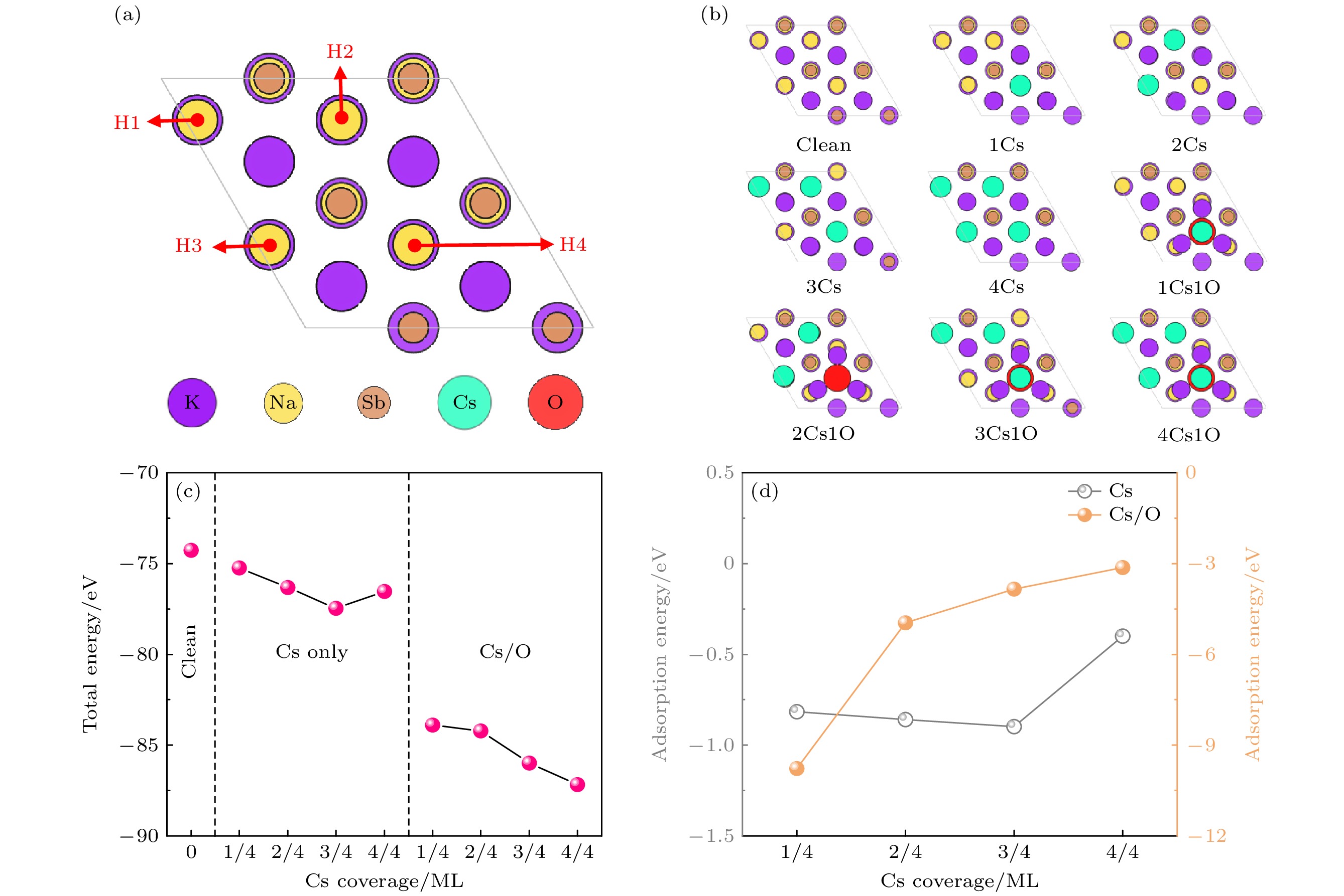
图 2 (a) Na2KSb (111) K表面的Cs, O原子吸附位; (b) 不同Cs/O覆盖度的吸附表面模型; (c) 不同吸附模型的总能量; (d) 不同吸附模型的Cs吸附能
Figure 2. (a) Adsorption sites for Cs atoms and O atoms on Na2KSb (111) K surface; (b) adsorption surface models with different Cs/O coverages; (c) the total energies of different adsorption models; (d) the adsorption energies of isolated Cs atom of different adsorption models.

图 3 Na2KSb (111) K表面Cs吸附和Cs/O吸附前后的 (a) Hartree静电势和 (b) 功函数和亲和势
Figure 3. (a) Hartree electrostatic potential and (b) work function and electron affinity for the Na2KSb (111) K surfaces before and after adsorption of Cs and Cs/O.

图 4 CDD俯视图和侧视图(蓝色和黄色区域分别代表电荷的积累和耗尽)
Figure 4. Top and side views of CDD (the blue and yellow regions represent the charge accumulation and charge depletion, respectively).

图 5 (a) 平均偶极子电荷量变化; (b) 平均偶极子长度变化; (c) 表面偶极矩和功函数变化
Figure 5. (a) Changes of average dipole charge; (b) changes of the average dipole length; (c) changes of surface dipole moment and work function.

图 6 (a) 清洁表面能带结构; (b) Cs覆盖表面能带结构(Cs覆盖度: 2/4 ML, 紫红色曲线表示Cs吸附产生的能带贡献); (c) Cs覆盖表面的Cs原子6s轨道PDOS; (d) Cs/O覆盖表面能带结构(Cs覆盖度: 2/4 ML, O覆盖度: 1/4 ML, 紫红色曲线表示Cs/O吸附产生的能带贡献); (e) Cs/O覆盖表面的Cs原子6s轨道PDOS; (f) Cs/O覆盖表面的O原子2p轨道PDOS
Figure 6. (a) Band structure for clean surface; (b) band structure for Cs-covered surface (Cs coverage: 2/4 ML, the magenta curve represents the energy band contribution from Cs adsorption); (c) PDOS of the 6s orbit of Cs atoms on the Cs-covered surface; (d) band structure for Cs/O-covered surface (Cs coverage: 2/4 ML, O coverage: 1/4 ML, the magenta curve represents the energy band contribution from Cs/O adsorption); (e) PDOS of the 6s orbit of Cs atoms on the Cs/O-covered surface; (f) PDOS of 2p orbit of O atom on the Cs/O-covered surface.

图 7 不同Cs覆盖度下表面模型的光学性质 (a) 折射率; (b) 消光系数
Figure 7. Optical properties of adsorption surface models with different Cs coverages: (a) Refractive index; (b) extinction coefficient.
-
[1] Hamamatsu Photonics K. K. https://www.hamamatsu.com/content/dam/hamamatsu-photonics/sites/documents/99_SALES_LIBRARY/etd/PMT_handbook_v4E.pdf [2023-6-1]
[2] Trucchi D M, Melosh N A 2017 MRS Bull. 42 488
Google Scholar
[3] 田丽萍, 李立立, 温文龙, 王兴, 陈萍, 卢裕, 王俊锋, 赵卫, 田进寿 2018 物理学报 67 188501
Google Scholar
Tian L P, Li L L, Wen W L, Wang X, Chen P, Lu Y, Wang J F, Zhao W, Tian J S 2018 Acta Phys. Sin. 67 188501
Google Scholar
[4] Maxson J, Cultrera L, Gulliford C, Bazarov I 2015 Appl. Phys. Lett. 106 234102
Google Scholar
[5] Wang Y, Mamun M A, Adderley P, et al. 2020 Phys. Rev. Accel. Beams 23 103401
Google Scholar
[6] Cultrera L, Gulliford C, Bartnik A, Lee H, Bazarov I 2016 Appl. Phys Lett. 108 134105
Google Scholar
[7] Yang B 1989 Appl. Phys Lett. 54 2548
Google Scholar
[8] Rusetsky V S, Golyashov V A, Eremeev S V, et al. 2022 Phys. Rev. Lett. 129 166802
Google Scholar
[9] Erjavec B 1994 Vacuum 45 617
Google Scholar
[10] Galan L, Bates Jr C W 1981 J. Phys. D: Appl. Phys. 14 293
[11] Dolizy P 1980 Vacuum 30 489
Google Scholar
[12] McCarroll W H, Paff R J, Sommer A H 1971 J. Appl. Phys. 42 569
Google Scholar
[13] Erjavec B 1996 Appl. Surf. Sci. 103 343
Google Scholar
[14] Guo T L, Gao H R 1991 Appl. Phys. Lett. 58 1757
Google Scholar
[15] Guo T L, Gao H R 1993 Appl. Surf. Sci. 70 355
[16] Guo T L 1996 Thin Solid Films 281 379
[17] Cultrera L, Karkare S, Lillard B, et al. 2013 Appl. Phys Lett. 103 103504
Google Scholar
[18] Cultrera L, Lee H, Bazarov I 2016 J. Vac. Sci. Technol. , B 34 011202
Google Scholar
[19] Ettema A R H F, Groot R A 2000 Phys. Rev. B 61 10035
Google Scholar
[20] Murtaza G, Ullah M, Ullah N, Rani M, et al. 2016 Bull. Mater. Sci. 39 1581
Google Scholar
[21] Amador R, Saßnick H D, Cocchi C 2021 J. Phys. Condens. Matter 33 365502
Google Scholar
[22] Schier R, Saßnick H D, Cocchi C 2022 Phys. Rev. Mater. 6 125001
Google Scholar
[23] Wang X C, Zhang K M, Jin M C, Ren L, Han Y F, Wang Q L, Zhang Y J 2022 Solid State Commun. 356 114960
Google Scholar
[24] Wang G X, Pandey R, Moody N A, Batista E R 2017 J. Phys. Chem. C 121 8399
[25] Shen Y, Yang X D, Bian Y, Chen L, Tang K, Wan J G, Zhang R, Zheng Y D, Gu S L 2018 Appl. Surf. Sci. 457 150
Google Scholar
[26] 向世明, 倪国强 1999 光电子成像器件原理 (北京: 国防工业出版社) 第291页
Xiang S M, Ni G Q 1999 The Principle of Optoelectronic Imaging Devices (Beijing: National Defense Industry Press) p291
[27] Karkare S, Boulet L, Singh A, Hennig R, Bazarov I 2015 Phys. Rev. B 91 035408
Google Scholar
[28] Shaltaf R, Mete E, Ellialtioglu S, 2005 Phys. Rev. B 72 205415
Google Scholar
[29] Hogan C, Paget D, Garreau Y, Sauvage M, Onida G, Reining L, Chiaradia P, Corradini V 2003 Phys. Rev. B 68 205313
Google Scholar

 DownLoad:
Catalog
Metrics
- Abstract views: 408
- PDF Downloads: 26
- Cited By: 0
