


Vol. 71, No. 24 (2022)
2022-12-20
SPECIAL TOPIC—Recent advances in hardware, algorithms and software of quantum computers

EDITOR'S SUGGESTION
2022, 71 (24): 240302.
doi: 10.7498/aps.71.20221782
Abstract +

EDITOR'S SUGGESTION
2022, 71 (24): 240303.
doi: 10.7498/aps.71.20221825
Abstract +
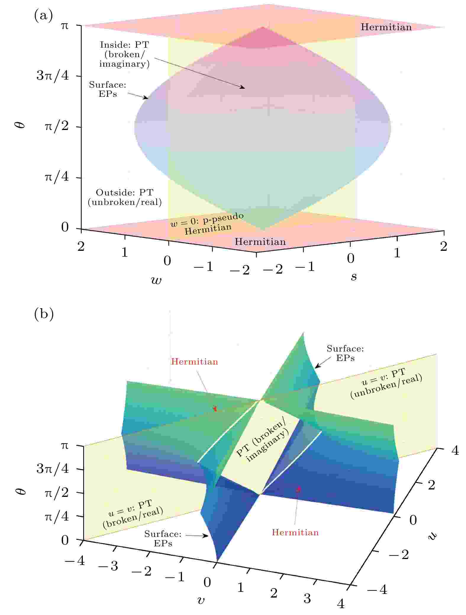
Quantum simulation is one of the main contents of quantum information science, aiming to simulate and investigate poorly controllable or unobtainable quantum systems by using controllable quantum systems. Quantum simulation can be implemented in quantum computers, quantum simulators, and small quantum devices. Non-Hermitian systems have aroused research interest increasingly in recent two decades. On one hand, non-Hermitian quantum theories can be seen as the complex extensions of the conventional quantum mechanics, and are closely related to open systems and dissipative systems. On the other hand, both quantum systems and classical systems can be constructed as non-Hermitian systems with novel properties, which can be used to improve the precision of precise measurements. However, a non-Hermitian system is more difficult to simulate than a Hermitian system in that the time evolution of it is no longer unitary. In this review, we introduce recent research progress of quantum simulations of non-Hermitian systems. We mainly introduce theoretical researches to simulate typical non-Hermitian quantum systems by using the linear combinations of unitaries, briefly showing the advantages and limitations of each proposal, and we briefly mention other theoretical simulation methods, such as quantum random walk, space embedded and dilation. Moreover, we briefly introduce the experimental quantum simulations of non-Hermitian systems and novel phenomena in nuclear magnetic resonance, quantum optics and photonics, classical systems, etc. The recent progress of the combinations of quantum simulation and non-Hermitian physics has promoted the development of the non-Hermitian theories, experiments and applications, and expand the scope of application of quantum simulations and quantum computers.
EDITOR'S SUGGESTION
2022, 71 (24): 240305.
doi: 10.7498/aps.71.20221824
Abstract +
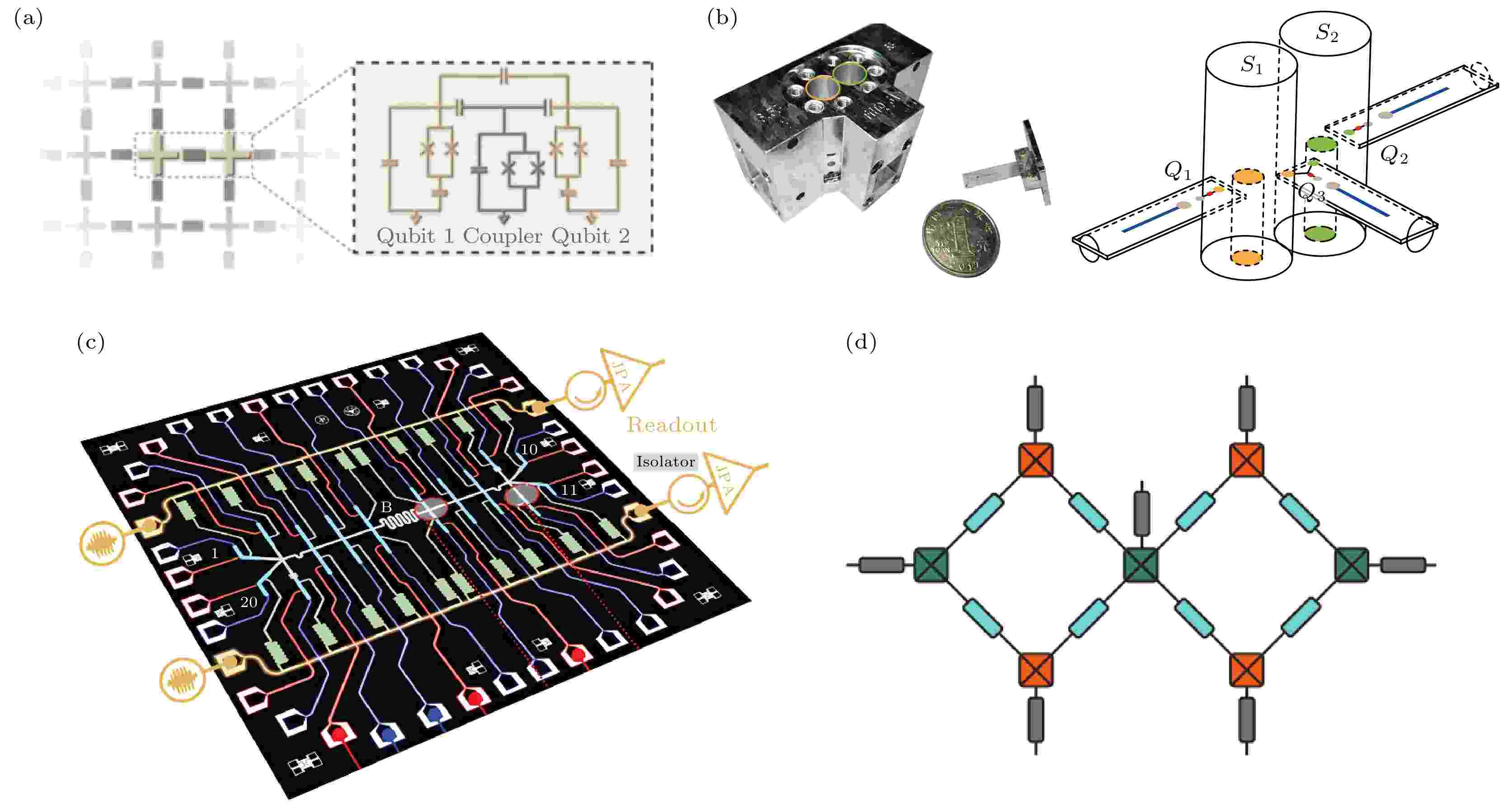
Information processing technology based on the basic principle of quantum mechanics shows great potential applications in computing, sensing and other fields, and is far superior to classical technology. With the advance of experimental technology, quantum control technology develops rapidly. Compared with other quantum information processing platforms, the superconducting system based on solid materials has the advantages of accurate quantum controllability, excellent quantum coherence and the potential for large-scale integration. Therefore, superconducting quantum system is one of the most promising platforms for quantum information processing. The existing superconducting circuits, which can integrate about one hundred qubits, have already demonstrated the advantages of quantum systems, but further development is limited by system noise. In order to break through this bottleneck, quantum error correction technology, which is developed from the classical error correction technology, has attracted extensive attention. Here, we mainly summarize the research progress of quantum error correction in superconducting quantum systems including the basic principles of superconducting quantum systems, the quantum error correction codes, the related control techniques and the recent applications. At the end of the article, we summarize seven key problems in this field.
EDITOR'S SUGGESTION
2022, 71 (24): 244207.
doi: 10.7498/aps.71.20221938
Abstract +
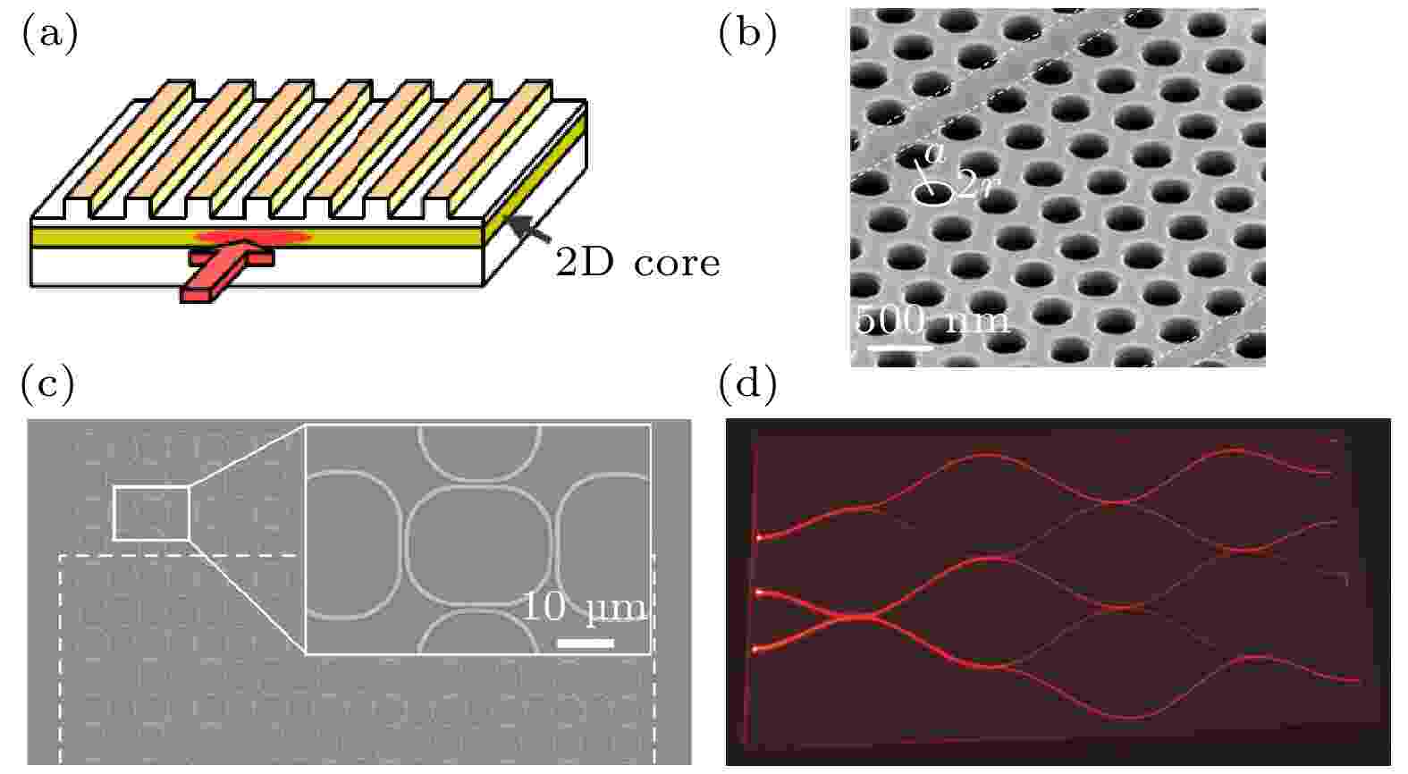
Quantum simulation is to use a controllable quantum system to simulate other complicated or hard-to-control quantum system, and to deal with some complex unknown quantum systems that cannot be simulated on classical computers due to the exponential explosion of the Hilbert space. Among different kinds of physical realizations of quantum simulation, integrated optical systems have emerged as an appropriate platform in recent years due to the advantages of flexible control, weak decoherence, and no interaction in optical systems. In this review, we attempt to introduce some of the basic models used for quantum simulation in integrated photonic systems. This review article is organized as follows. In Section 2, we introduce the commonly used material platforms for integrated quantum simulation, including the silicon-based, lithium niobate-based integrated circuits, and the femtosecond laser direct writing optical waveguides. Several integrated optical platforms such as the coupled waveguide arrays, photonic crystals, coupled resonator arrays, and multiport interferometers are also introduced. In Section 3, we focus on the analog quantum simulations in the integrated photonic platform, including Anderson localization of light in disordered systems, various kinds of topological insulators, nonlinear and non-Hermitian systems. More specifically, in Subsection 3.1, we present the integrated photonic realizations of disordered and quasi-periodic systems. In Subsection 3.2, we review the integrated photonic realizations of the topological insulators with and without time-reversal symmetry, including Floquet topological insulators, quantum spin hall system, anomalous quantum hall system, valley hall system, Su-Schrieffer-Heeger (SSH) model, and photonic topological Anderson insulators. Besides, topological insulator lasers and topologically protected quantum photon sources are briefly reviewed. In Subsection 3.3, we review the nonlinear and non-Hermitian integrated optical systems. In Section 4 we present the integrated digital quantum simulations based on the multiport interferometers, including the discrete-time quantum random walk, Boson sampling, and molecular simulation. In Section 5, we summarize the content of the article and present the outlook on the future perspectives of the integrated photonic quantum simulation. We believe that the integrated photonic platforms will continue to provide an excellent platform for quantum simulation. More practical applications will be found based on this system through combining the fields of topological photonics, laser technologies, quantum information, nonlinear and non-Hermitian physics.
SPECIAL TOPIC—Frontiers in non-Hermitian physics
EDITOR'S SUGGESTION
2022, 71 (24): 247802.
doi: 10.7498/aps.71.20221706
Abstract +
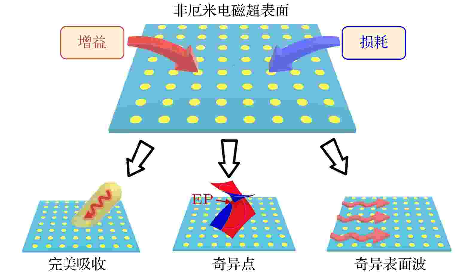
Electromagnetic metasurface, as a type of planar electromagnetic material consisting of single-layer or multilayer subwavelength artificial micro-structure, can efficiently control the polarization, amplitude and phase of electromagnetic wave on a subwavelength scale. However, confining electromagnetic waves to a deep-subwavelength scale generally is at the cost of a large loss, such as radiation loss, Ohmic loss. Interestingly, non-Hermitian physics provides us a new way to transform the disadvantage of loss into a new degree of freedom in metasurface design, paving the way to expanding the functionalities of metasurfaces. In recent years, the extraordinary effects in the non-Hermitian electromagnetic metasurfaces have attracted a lot of attention. In this review, we discuss the perfect absorption, exceptional points and surfaces waves of non-Hermitian electromagnetic metasurfaces, and point out the challenges and potentials in this field.
REVIEW
2022, 71 (24): 240701.
doi: 10.7498/aps.71.20221462
Abstract +
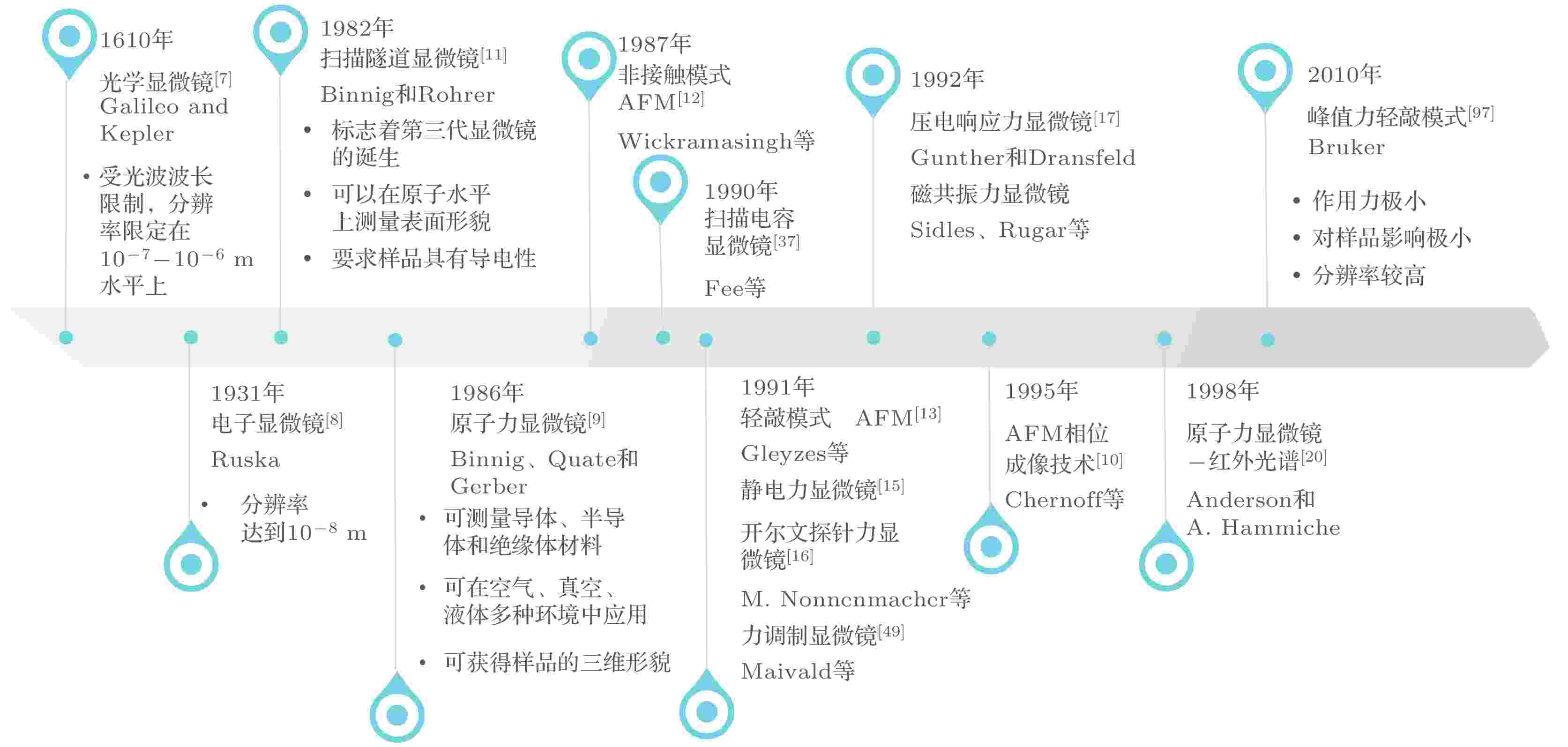
The rapid development of the electrical and electronic industry requires components with miniaturization, flexibility, and intelligence. Dielectric materials, as important materials for the preparation of electronic components, are required to have excellent dielectric properties such as high breakdown electric field, high energy storage density and low dielectric loss. Owing to the lack of ultra-high resolution characterization tools, the research on the improvement of dielectric material properties stopped at a macroscopic level in the past. Atomic force microscopy, a measurement instrument which possesses a nanoscale high resolution, shows unique advantages in the study of nanodielectrics, and the advent of functional atomic force microscopy has made important contributions to characterization of the electrical, optical, and mechanical properties of nano-dielectric micro-regions. In this paper, we review the progress of atomic force microscopy, electrostatic force microscopy, Kelvin probe force microscopy, piezoelectric response force microscopy and atomic microscopy-infrared spectroscopy in the study of nanodielectric applications. Firstly, their structures and principles are introduced; secondly, their recent research progress of studying the microscopic morphology, interfacial structure, domain behavior and charge distribution in the nanometer region of dielectric materials is presented, and finally, the problems in the existing research and possible future research directions are discussed.
GENERAL

EDITOR'S SUGGESTION
2022, 71 (24): 240301.
doi: 10.7498/aps.71.20221055
Abstract +
In the framework of the electronic tight-binding model of order-disorder separated (ODS) bilayer square lattice (BSL) and by calculating the density of states (DOS), participation number of eigen-wavefunctions and quantum diffusion, we systematically study the effects of stacking interface structure, strength of interlayer coupling and degree of disorder on the electron transport properties of order-disorder separated two-dimensional bilayer systems. Our results show that for the ODS-BSL of AA-stacking in the regime of weak coupling, the ODS-BSL always possesses a single energy band with localized states in its band tail, and extended states or critical states similar to the extended ones in the band center region with persistent metal-insulator transitions and associated mobility edges under strong disorder. In the regime of strong coupling, weak disorder leads the critical states to exist in its band tails and extended states to occur in the band center regions, while strong disorder results in the formation of a single band due to the overlapping of the coupling-induced two bands with localized states in the band tails and critical states in the band center region with increasing participation numbers as disorder increases. The ODS-BSL of AB-stacking always possesses a single band and supports extended states and critical states in its band center region, regardless of the strengths of interlayer coupling and disorder. In both ODS-BSL systems of AA- and AB- stackings, quantum diffusion undergoes an anomalous transition from weakening to enhancing behaviors as disorder increases. In the AA-stacking ODS-BSL of weak coupling, AA-stacking ODS-BSL of weak disorder and the AB-stacking ODS-BSL, quantum diffusion exhibits super-diffusion due to the contribution of extended states and the critical states similar to extended ones. In the AA-stacking ODS-BSL of strong coupling, quantum diffusion undergoes sub-diffusion under strong disorder due to the existence of critical states. The numerical results also show that the order-disorder separated (ODS) bilayer hexagonal lattice exhibits the same behaviors as those revealed in ODS-BSL systems.
EDITOR'S SUGGESTION
2022, 71 (24): 240304.
doi: 10.7498/aps.71.20221072
Abstract +
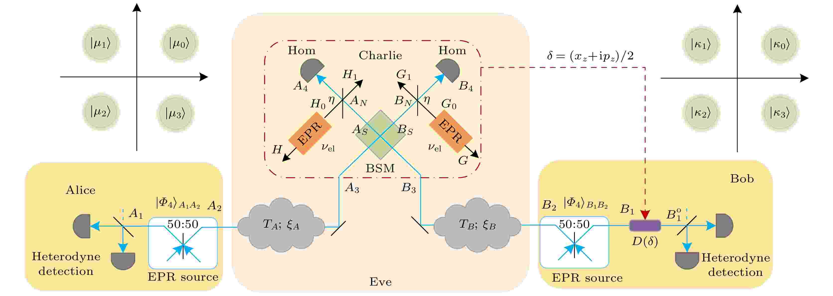
Discrete modulation continuous variable measurement device independent quantum key distribution scheme has good compatibility with efficient error correction codes, which leads to high reconciliation efficiency even at low signal-to-noise ratio. Besides, the implementation of this protocol is simpler than that of Gaussian modulation scheme. However, the quantum efficiency of homodyne detector commonly used in the experiment is only 0.6, which will seriously affect the practical application performance of discrete modulation continuous variable measurement device independent quantum key distribution scheme. To solve this problem, we propose a discrete modulation continuous variable measurement device independent quantum key distribution scheme based on realistic detector compensation. In our scheme, for the outputs of two quantum channels, each adopts a phase sensitive amplifier to compensate for the corresponding realistic homodyne detector. The simulation results show that the phase sensitive amplifier can well compensate for the quantum efficiency of the realistic detector and effectively improve the performance of the discrete modulation continuous variable measurement device independent quantum key distribution scheme with realistic detector in terms of secret key rate and secure transmission distance. The proposed protocol provides an effective method for promoting the practical development of the discrete modulation continuous variable measurement device independent quantum key distribution scheme.
2022, 71 (24): 240501.
doi: 10.7498/aps.71.20221367
Abstract +
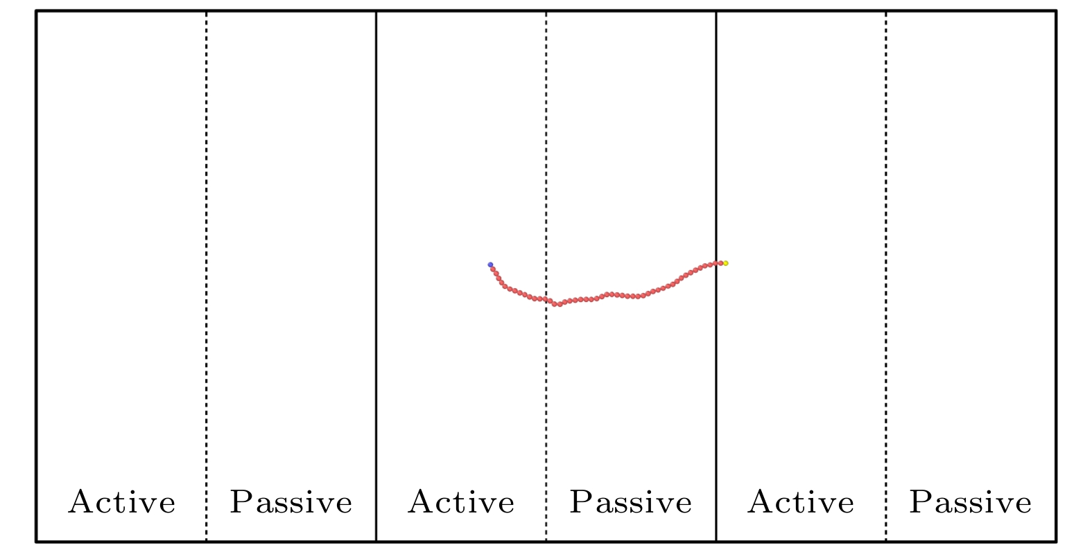
Active polymers exhibit very rich dynamic behaviors due to their deformable long-chain architecture. In this work, we perform Langevin dynamics simulations to study the behavior of a single self-propelled polymer chain in a plane (two dimensions) whose activity can be tuned by external field. We consider a spatially on-off periodic field along the x direction, i.e. the plane is patterned into stripes of alternating active region and passive region. The width d of the stripe (half period length) plays a key role in determining the kinetic behavior of a flexible polymer chain. When $ d\gg 2{R}_{\rm{g}0} $ ($ {R}_{\rm{g}0} $ is the radius of gyration of the passive flexible chain in the random coil state), the polymer chain can stay for a long time in either the active region or the passive region and moves mainly by slow Brownian diffusion; when $ 2{R}_{\rm{L}} < d < 2{R}_{\rm{g}0} $ ($ {R}_{\rm{L}} $ is the radius of the spiral formed by the self-propelled polymer chain), the polymer chain could stay entirely in one region but cross-regional motion happens frequently; when $ d < 2{R}_{\rm{L}} $ , the polymer chain does not stay entirely in one region but keeps moving cross-regionally accompanied by the stretching of the parts in active regions. With the kinetic behavior of the polymer chain changing as d varies, the long-time diffusive coefficient changes by as great as two orders of magnitude and other statistical quantities such as spatial density distribution, mean total propelling force, characteristic size and orientation all show non-monotonic variations. In addition, we find four typical processes of the cross-regional motion of a flexible chain. For a semiflexible polymer chain, the cross-regional motion is accompanied by buckling behavior and the width d affects greatly the degree of buckling and the continuity of the motion. Our work suggests a new idea for tuning and controlling the dynamic behavior of active polymers and provides a reference for the design and the potential applications of chain-like active materials.


2022, 71 (24): 240502.
doi: 10.7498/aps.71.20221423
Abstract +
2022, 71 (24): 240601.
doi: 10.7498/aps.71.20221469
Abstract +
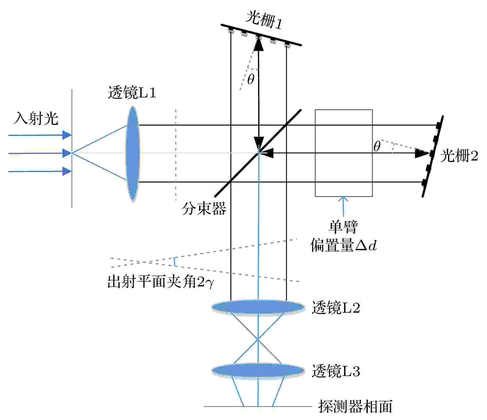
Asymmetric spatial heterodyne spectroscopy is a new ultra-high resolution remote sensing detection technology. Based on its features of large luminous flux, small size, and high precision, it is very suitable for high-precision detection in a deep-space environment. Because of its high sensitivity, various details may interfere with the measurement results in experiment. In this paper, from the perspective of experimental condition, considering the influences of factors such as fringe center position offset, uneven illumination, and Gaussian noise, a compound optical path difference phase-shift solution method is proposed. The simulation calculation and data analysis show that the offset of the nominal point relative to the center position will significantly affect the systematic error of spectral velocity measurement. And the compound optical path difference phase-shift solution method can smooth the environmental noise and random interference to a certain extent. For the interference fringe image with 1% Gaussian noise, the velocity measurement error can be controlled within 5‰ by using the compound optical path difference phase-shift solution method, which makes the asymmetric spatial heterodyne spectroscopy technology more suitable for space optoelectronic precision measurement.
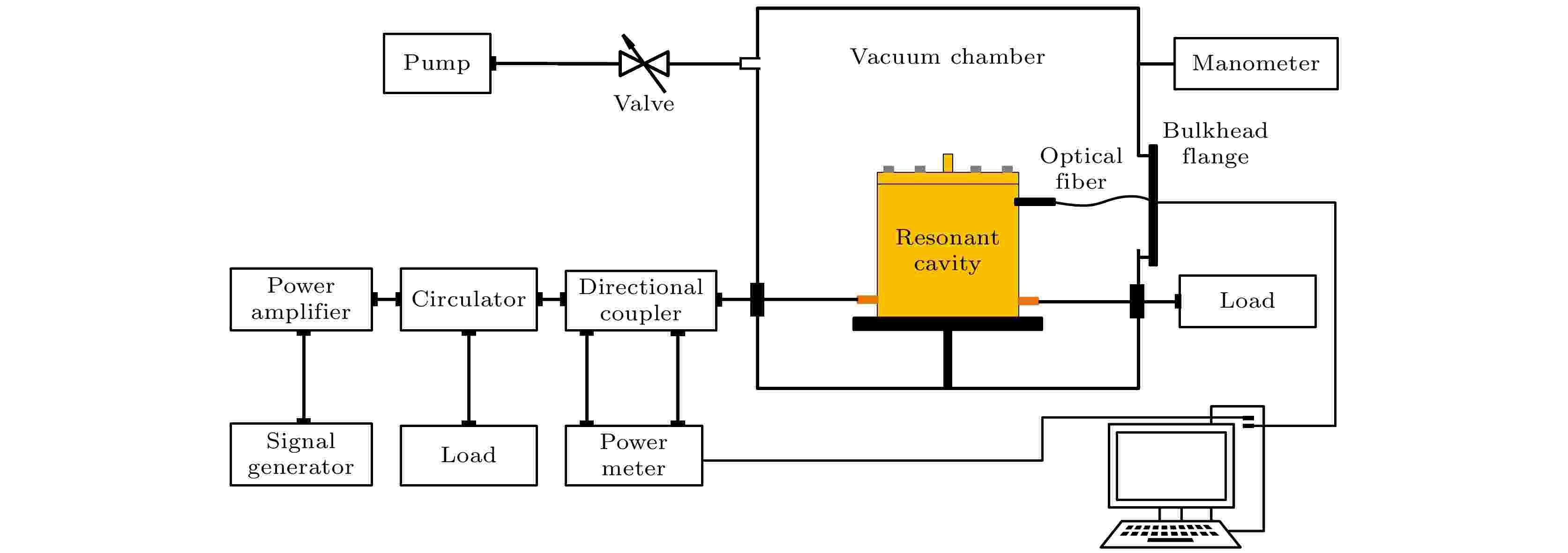
2022, 71 (24): 240702.
doi: 10.7498/aps.71.20221385
Abstract +
Low-pressure discharge is an important problem that restricts the development of microwave components of spacecraft toward high-power and miniaturization. To clarify the mechanism of low-pressure discharge of microwave component in spacecraft, we build an emission spectroscopy diagnostic platform for studying the low-pressure radio frequency (RF) discharge plasma, and investigate the plasma reaction dynamics of low-pressure RF discharge of microwave cavity resonator and the damage effect of discharge on microwave component. The emission spectra of the plasma inside the resonator under different gas pressure conditions are obtained, and it is found that the density of hydroxyl OH (A-X), excited nitrogen molecules N2 (C-B) and oxygen atoms O (3p5P→3s5S0) in the plasma each show a first-increasing and then decreasing trend with the increase of gas pressure. The kinetic mechanism of the plasma reaction behind this phenomenon is analyzed, and it is found that the gas pressure can influence the concentration magnitude of each species in the plasma by changing the species production and consumption paths as well as the average electron temperature of the plasma. The variation law of plasma emission spectrum with the input power is studied, and the trends of linear increase of particle concentration with the increase of input power at different air pressures are found. This study provides a reference for investigating the mechanism of low-pressure RF discharge and the reliable design of spacecraft microwave components.
ATOMIC AND MOLECULAR PHYSICS
2022, 71 (24): 243101.
doi: 10.7498/aps.71.20221368
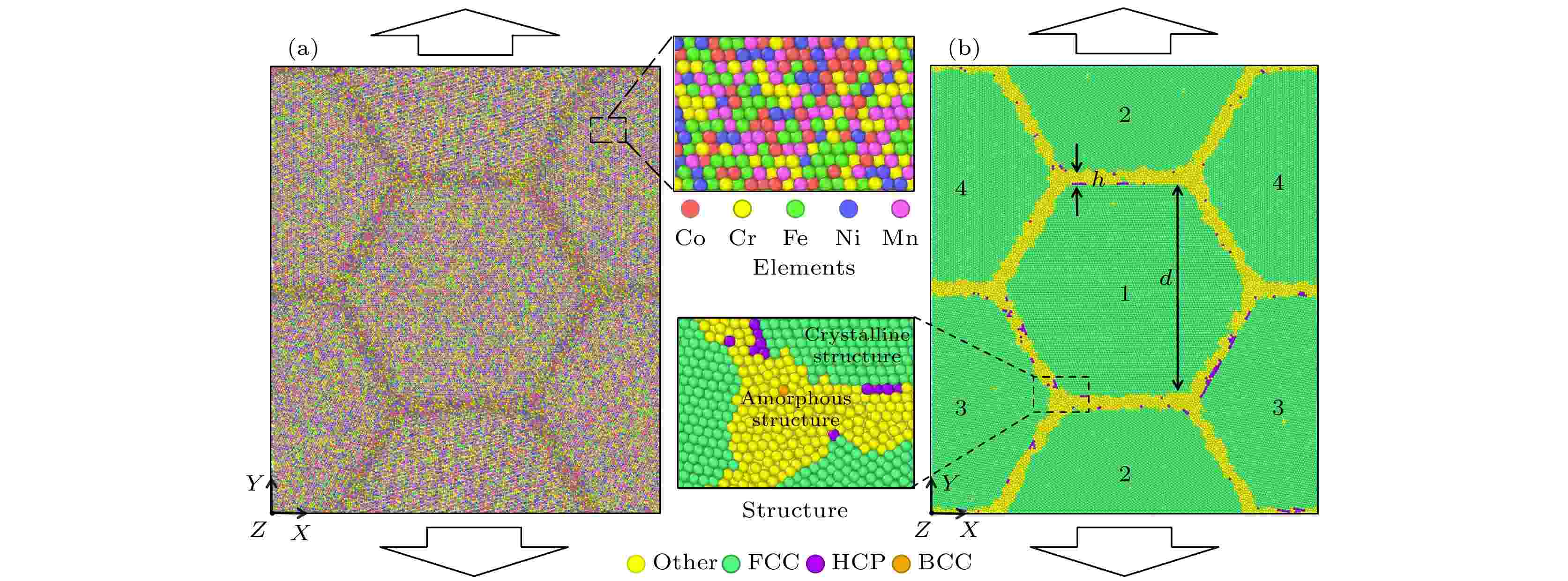
Abstract +
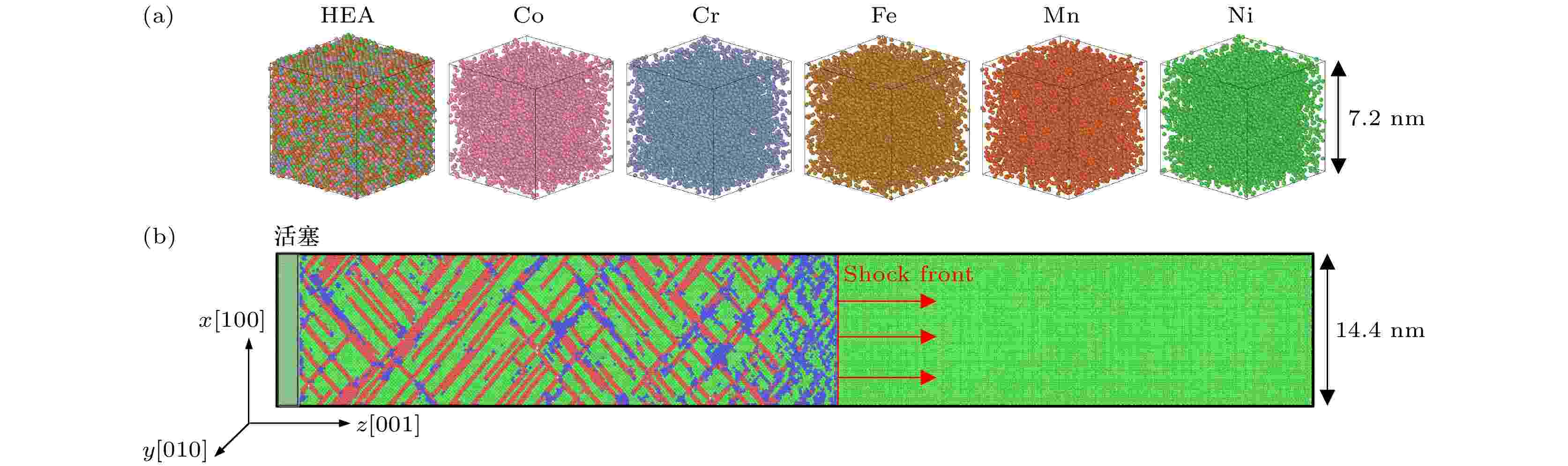
Recently proposed crystalline/amorphous dual-phase high-entropy alloy is an effective strategy to obtain high-entropy, high-strength and high-toughness alloys. And the relative plastic deformation mechanism is dependent on the size of component phases. The effect of component phase size on the plastic deformation mechanism of CoCrFeNiMn crystalline/amorphous dual-phase high-entropy alloy is investigated by molecular dynamics simulation. The results indicate that the size of amorphous phase has a significant effect on the mechanical behavior and plastic deformation mechanism of high entropy alloy. For the sample with small thickness of amorphous phase, the plastic deformation is dominated by dislocation slip and phase transformation of face-centered-cubic structure to hexagonal-close-packed structure. Especially, the deformation twins and Lomer-Cottrell locks are observed in the sample with amorphous layer spacing of 1 nm. When the thickness of the amorphous layer is moderate, the plastic deformation of the dual-phase high-entropy alloy is realized mainly through the dislocation slip, phase transformation of face-centered-cubic structure to hexagonal-close-packed structure in crystalline part and shear band multiplication in amorphous part. If the amorphous layer spacing is larger, the plastic deformation of the high-entropy alloy is dominated by the formation of uniform shear bands in the amorphous phase. In addition, the amorphous phase in the dual-phase high-entropy alloy structure can stabilize the crystalline grains. The results of this study can provide a guidance for designing and preparing high entropy alloy with high performance.
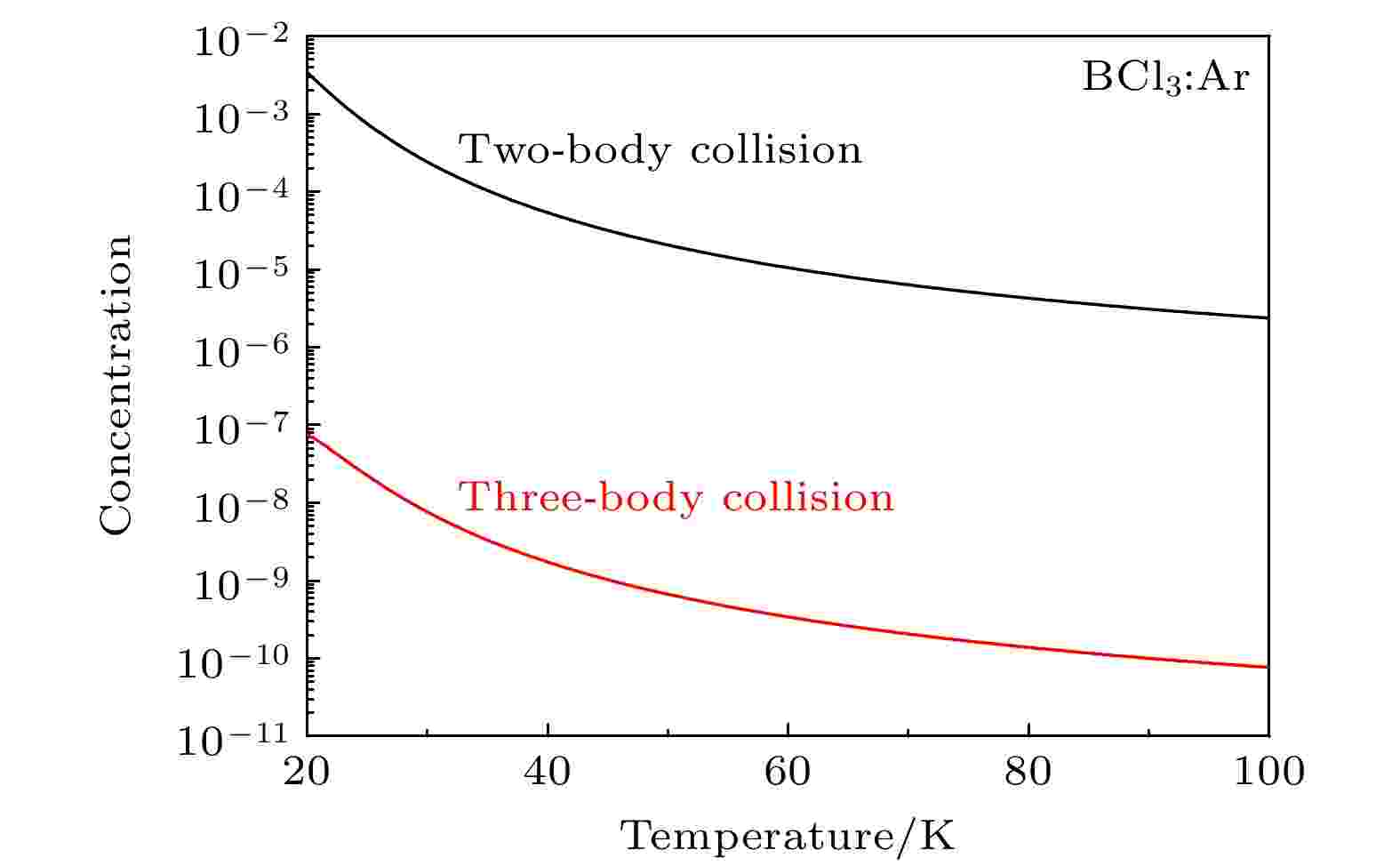
2022, 71 (24): 243401.
doi: 10.7498/aps.71.20221517
Abstract +
In the low temperature environment generated by supersonic flow in the process of laser assisted retardation of condensation of isotope separation for BCl3, the molecular isotopes BCl3 and carrier gas (rare gas (RG): He, Ne, Ar, Kr, Xe) can form BCl3:RG dimer via contact collision process. The mechanism and relationship between dimer concentration and absolute temperature of dimer involving BCl3 molecules are of great significance for regulating and selecting the isotope separation parameters. In this work, based on the analytic description of the anharmonic interaction potential function of BCl3:RG, and considering the two-body and three-body collision induced association and dissociation of dimers, the concentration of BCl3:RG dimers is obtained at the absolute temperature in a range of 20–40 K. The obtained results are as follows. The two-body collision is dominant in the formation of dimer in the low temperature range. When the initial molar fraction of BCl3 is in a range of 0.01–0.10, the BCl3:RG dimer concentration changes approximately linearly with the initial molar fraction of BCl3, indicating that the initial molar fraction not only determines the theoretical upper limit of the dimer concentration, but also dominates the dimer concentration in a low temperature range. When the temperature of the supersonic flow chamber is about 20 K, the concentration of BCl3:Kr dimers is largest, and the concentrations of other dimers are also presented. Furthermore, we explain the mechanism of laser assisted retardation of condensation in separation of isotopes by using a simple model on a molecular scale by adjusting the parameters of dissociation energy and stretching vibration frequency of the dimer.
ELECTROMAGNETISM, OPTICS, ACOUSTICS, HEAT TRANSFER, CLASSICAL MECHANICS, AND FLUID DYNAMICS
Three-band plasmon induced transparency effect based on four-disk resonator coupled waveguide system
2022, 71 (24): 244201.
doi: 10.7498/aps.71.20221397
Abstract +
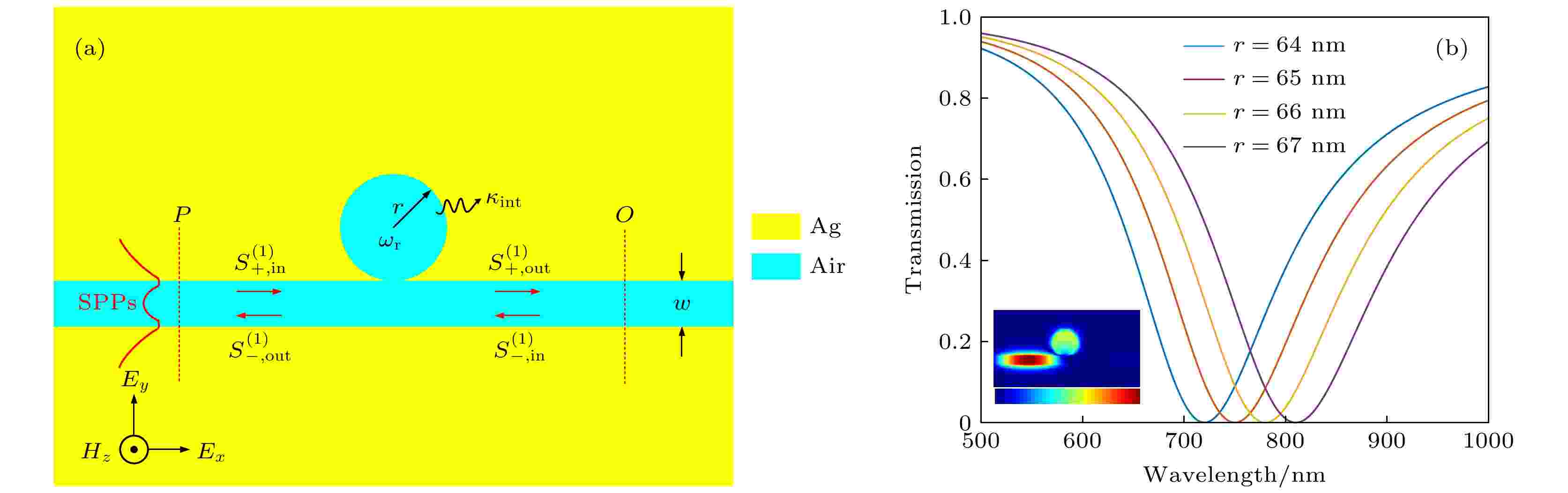
In order to reduce power consumption and realize ultrafast response time and dynamic tunability, a plasmonic waveguide system based on four disk resonators is designed. A plasmon induced transparency effect is theoretically analyzed by using two different methods: one is the direct destructive interference between bright mode resonator and dark mode resonator, and the other is the indirect coupling through a plasmonic waveguide. Owing to the giant effective nonlinear Kerr coefficient of the graphene-Ag composite material structure and the enhancement characteristics of slow light response to optical Kerr effect, the pump intensity of PIT system for changing the phase shift of transmission spectrum is greatly reduced. An ultrafast response time of 1 ps is achieved, and 0.4π, 0.8π, 1.2π, 1.6π and 2π-phase shift of the transmission spectrum in the plasmon induced transparency system are achieved with the intensity of the pump light as low as 2.34, 4.68, 7.02, 9.36, 11.7 MW/cm–2, respectively. In this work, a plasmonic waveguide coupled directly by two small disk resonators is employed, because two small disk resonators play a role of the slit between the waveguide and the resonators, and also act as two separate resonators side-coupled with a plasmonic waveguide, which leads to the more efficient coupling of electromagnetic energy in the waveguide into the big disk resonators to form resonance and easier storage of light in the resonator. The triple-band plasmon induced transparency (PIT) effect and slow light properties of the model are analyzed by the expression of the deduced theoretical transmittance based on the coupled mode theory, indicating that they are very consistent with the finite-difference time-domain simulations. The results show that the transmission peak of the system is over 80% and the maximum group index is as high as 368. Furthermore, the disk resonators are easy to fabricate and the size of the entire PIT structure is < 0.5 μm2, which is beneficial to the design of optoelectronic device on-chip integration. The research results have important application prospects in highly integrating optical circuits and networks, and also provide the ideas for the design and fabrication of multi-channel optical filter and light storage devices with low power consumption, ultrafast nonlinear response, ultracompact and dynamical tunability.
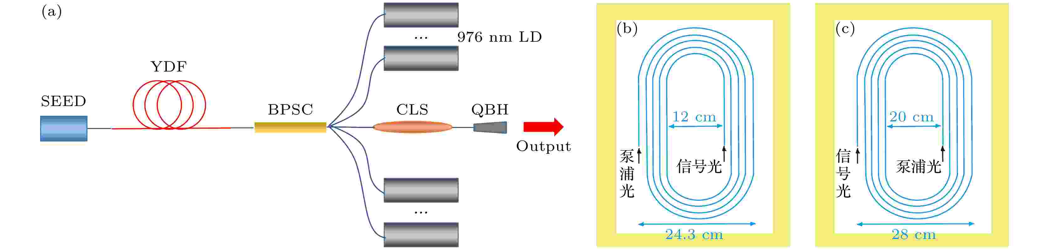
2022, 71 (24): 244202.
doi: 10.7498/aps.71.20221433
Abstract +
Fiber lasers have been widely used in the industrial and scientific fields due to their advantages of high conversion efficiency, simple thermal management, and consistent stability. High brightness and high-power fiber lasers are affected by stimulated Raman scattering and transverse mode instability, which limits the power scaling of fiber lasers. Therefore, there are only a few researches achieving a 10 kW-level fiber laser system by laser diode direct pumping or tandem pumping. In this work, we demonstrate an all-fiber laser amplifier based on home-made low numerical aperture (NA) fiber pumped by 976 nm laser diodes. When the signal light is input to the gain fiber with a minimum bending diameter of 12 cm, the beam quality factor M2 is about 1.72. The onset of transverse mode instability (TMI) is observed at 2467 W output power, accompanied by beam quality degradation. In order to suppress the onset of TMI, the minimum bending diameter of the gain fiber is changed from 12 cm to 20 cm. And the signal light is input into the gain fiber with a bending diameter of 28 cm. Benefiting from this operation, the fiber laser amplifier achieves maximum output power of 10.53 kW with an optical-to-optical efficiency of 74.04%, and there is no TMI onset observed. However, increasing bending diameter inevitably leads the beam quality to degrade. At the maximum output power, the beam quality factor M2 is 2.88. To the best of our knowledge, this is the highest optical-to-optical efficiency and the best beam quality in 10 kW-level laser diodes pumping fiber lasers. Generally, it is believed that reducing bending diameter can suppress TMI by increasing high-order mode loss. However, this rule is not applicable to few-mode fiber lasers. A larger bending diameter leads more high-order modes to be contained in the signal light instead of leaking into the cladding area. Thus, a higher output and poor beam quality are obtained. Also, it is believed that tightly coiled fiber can make mode coupling easier and trigger off TMI, which results in a positive correlation between the TMI threshold and bending diameter. Low NA fibers are very sensitive to bending, and reducing the bend diameter to control the beam quality will result in lower efficiency and a lower TMI threshold. Therefore, although producing a 10 kW-level fiber laser is simple, maintaining good beam quality in the power scaling process is still a challenge. The results of this study will be a valuable reference for high power fiber laser design.
2022, 71 (24): 244203.
doi: 10.7498/aps.71.20221518
Abstract +
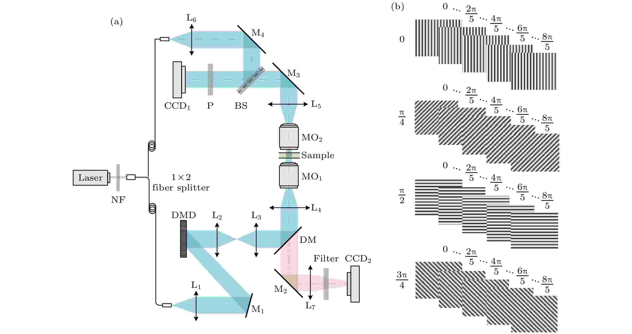
Quantitative phase microscopy (QPM) is a label-free imaging technique often employed for long-term, high-contrast imaging of live bio-samples. Yet, QPM is not specific to a certain subcellular organelle. As a remedy, fluorescence microscopy can visualize specific subcellular organelles once being labeled with fluorescent markers. In this paper, a high-resolution phase/fluorescence dual-modality microscopic imaging method based on structured light illumination is proposed. In a dual-modality microscopic system, periodic stripes are generated by a digital micromirror array (DMD), and are used as the common illumination for both modalities. For QPM imaging, the holograms of the sample under structured light illuminations from different directions and phase shifts are recorded, from which a quantitative phase image with resolution enhancement can be reconstructed via a synthetic aperture procedure. Furthermore, a numerical approach is proposed to compensate for the environmental disturbances that often challenge aperture synthesis of phase imaging. This method determines each time the phase distortions caused by environmental disturbances through using the spectrum of the 0th order of the structured light illumination, and the phase distortions are removed from the phase distributions of the waves along the 0th and the ±1st diffraction orders. Resolution enhancement of QPM imaging is realized by synthesizing the spectra of all the waves along different diffraction orders of the structured light illuminations of different orientations. With phase images, three-dimensional shapes, inner structures, or refractive index distributions of transparent and translucent samples can be obtained. For fluorescence imaging, intensity images (morie patterns) of the sample under different structured light illuminations are recorded. The spectra along different diffraction orders are separated by using a phase shifting reconstruction algorithm, and are shifted to their original positions, forming a synthesized spectrum that is much broader than the spectra of raw intensity images (NA-limited spectra). An inverse Fourier transform on the synthesized spectrum yields a super-resolution fluorescence image of the sample. With the reconstructed fluorescence images, specific subcellular organelles labeled with fluorescent markers can be visualized. The combination of quantitative phase microscopy and fluorescence microscopy can obtain multidimensional information about the sample. In this dual-mode imaging system, the spatial resolution of quantitative phase imaging and fluorescence imaging are 840 nm and 440 nm, respectively. The proposed dual-mode microscopy imaging technique has been demonstrated for imaging fluorescent beads, fly wings, spring/rice leaves, mouse tail transection, and fluorescence-stained SiHa cells. We envisage that this method can be further applied to many fields, such as biomedicine, industry, and chemistry.
EDITOR'S SUGGESTION
Input-output characteristics of single-mode cavity with multiple coherently coupled artificial atoms
2022, 71 (24): 244204.
doi: 10.7498/aps.71.20221456
Abstract +
In previous cavity quantum electrodynamics (QED) systems, atomic gas is usually treated as single atoms, thereby resulting in phenomena such as Rabi splitting, and single-photon blocking. Benefiting from the development of superconducting circuit QED, the superconducting quantum interference devices (SQUIDs) can be regarded as artificial atoms, and the detuned coupling of them through LC harmonic oscillators will constitute an equivalent coherent coupling between artificial atoms. According to this, we study the effect of multiple artificial atoms with coherent coupling on the input and output of a single-mode cavity, and analyze the transmission spectrum from the perspective of decorated state. We find that single-mode cavities containing multiple artificial atoms with coherent coupling have significantly different transmittances from cavities containing single atoms, the transmission spectra of which are correlated with the coherent coupling coefficients between the artificial atoms, and the coupling coefficients between the cavity modes and the artificial atoms, and we also find that both the cavity mode leakage rate and the artificial atom decay rate are related to each other. And as the number of artificial atoms increases, the number of transmission peaks does not increase, and there are only three transmission peaks at most. In order to explain the law of this transmission spectrum, we quantize both artificial atoms and cavity modes, and calculate the eigenvalues and eigenstates of the whole in a single quantum case. In principle, if there are several particles, they will form several decorative states, and there will theoretically appear several transmission peaks. However, we find that there are some decorated states that do not contain the photonic component and thus do not contribute to the transmission peak. From the specific form of these decorated states, many of them have the property of many-body entanglement. Therefore, using such a single-mode cavity containing multiple coherently coupled artificial atoms, we can construct the required many-body entangled state by simply inputting weak monochromatic light, and at the same time, we can sense the forms of multi-body entanglement states in the cavity through the change of transmittance.
2022, 71 (24): 244205.
doi: 10.7498/aps.71.20221325
Abstract +
Precision measurement is an important direction of today’s frontier scientific research. Using lasers to achieve high-precision target measurement has become an important way to improve measurement accuracy, which can be used in various fields. However, for a certain application, the measurement accuracy will directly depend on the noise level of the laser source. Most of applications require that the measurement frequency band is concentrated in the audio frequency band. In order to obtain a low-noise laser source with shot noise limited in the applied frequency band, active and/or passive noise reduction is usually an option, i.e. active feedback control or filter cavity technique, etc. Therefore, noise analysis and suppression techniques are the main concern of the precision measurement. The optical filter cavity acts as an optical low-pass filter, which can effectively suppress high-frequency noise beyond its linewidth. In this work, we find that the intensity noise of the output field of an optical filter cavity is higher than the noise floor of the laser. The main sources of noise are analyzed experimentally, showing that 1) excess noise is introduced by cavity length locking, and 2) laser phase and pointing noises are coupled to the intensity one by the cavity. To cancel the excess noise as much as possible, we optimize the feedback control loop by measuring the open-loop and closed-loop transfer functions of the mode cleaner (MC), combined with the critical proportionality method. All the control loops are homemade, and the proportional-integral-derivative (PID) is designed with a field programmable gate array board for expediently achieving a noise reduction up to 30 dB at the audio frequency. Then the control loop is optimized to the best condition without introducing the excess noise. Compared with the free-running laser, MC filters out the high-frequency noise, meanwhile converts the phase noise and pointing noise of input field into the intensity noise of the output field. Therefore, the power noise spectrum in the audio band is still higher than that of the input optical field itself. In the future, an active control loop will be used to suppress the noise power. The experimental results provide the basic means for application research such as feedback control loop noise analysis, which will promote the development of precision measurement toward higher measurement accuracy.
2022, 71 (24): 244206.
doi: 10.7498/aps.71.20221618
Abstract +
2022, 71 (24): 244301.
doi: 10.7498/aps.71.20221504
Abstract +
2022, 71 (24): 244302.
doi: 10.7498/aps.71.20221292
Abstract +
The topological insulator, as its novel physical properties, such as transmission protection, energy loss free and defect immunity, has aroused much interest recently. It is necessary to introduce the concept of topology into elastic materials to enrich the research contents of elastic waves. The concept of valley state provides a simplest solution to realize topological states. In this work, we design a double surface periodic phononic crystal based on elastic material, the upper and lower surfaces are composed of periodically arranged triangular prismatic scatterers. Valley topological states of elastic phononic crystals are observed only when focusing on Lamb waves in out-of-plane mode by numerical simulation. We also analyze theoretically the valley Chern number. As the angle between the triangular prism and the positive direction of the X axis is greater than 0, the Chern number of K is 1/2; when the angle is less than 0, the Chern number is –1/2 . The K has the number opposite to the Chern number. By simply tuning the geometry of the scatterer, the inversion of the energy band will occur and the topological phase transition will be realized. We find that the frequency of edge state in valley topology can be regulated by adjusting the heights of scatterers. Moreover, wide frequency excitation is achieved at the edge interface composed of different valley Hall materials, which proves that the idea of adjustable edge state frequency can be implemented in elastic materials. According to the two different valley phase phononic crystals, we study the topological transport, exhibiting excellent transmission performance, even the Z-shaped interface. We find that the designed double surface structure has a stronger immune effect to defects than single surface, achieving a new degree of freedom in the valley topology protection of elastic wave excitation.
2022, 71 (24): 244303.
doi: 10.7498/aps.71.20221101
Abstract +
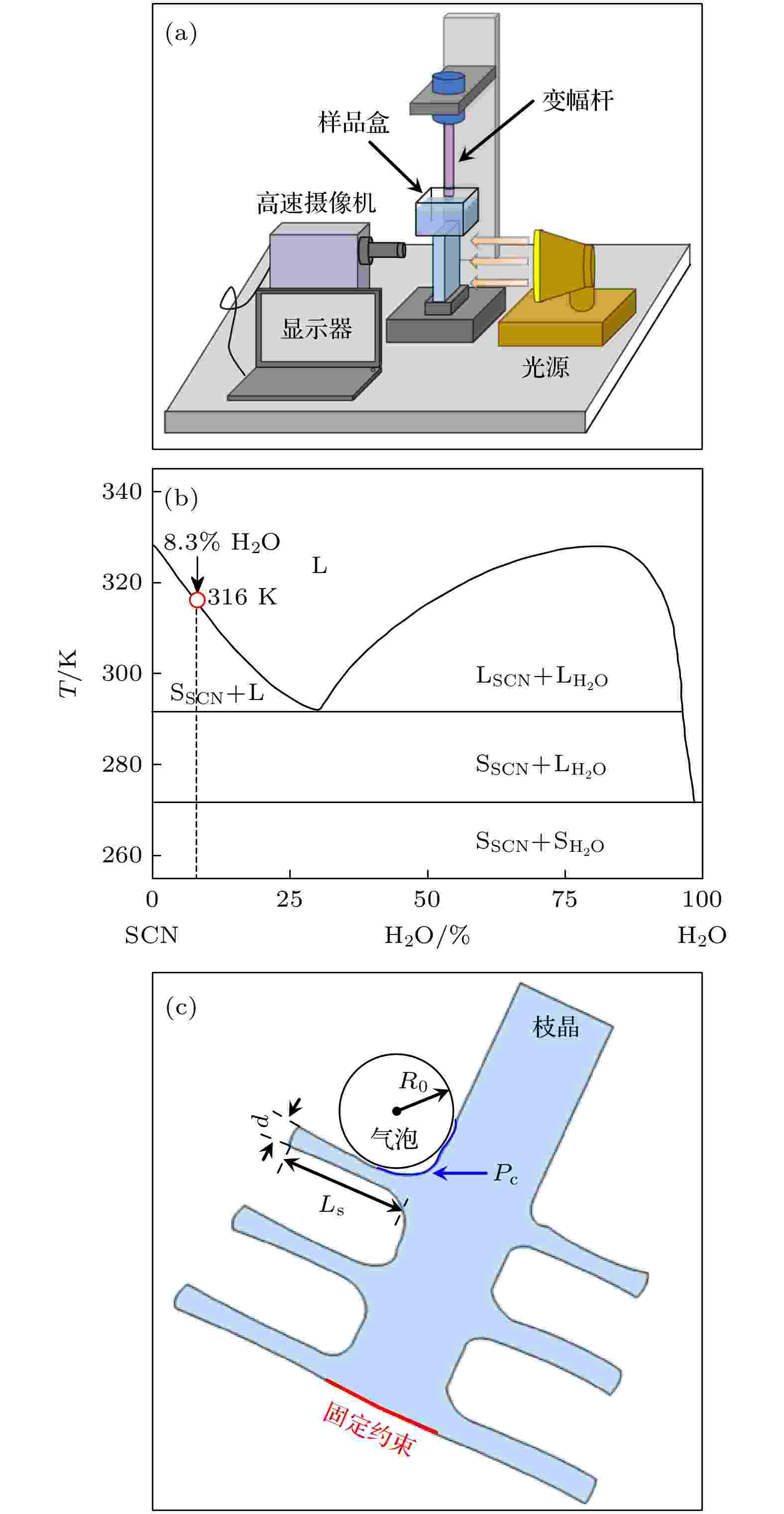
Ultrasonic waves used in liquid alloys can produce refined grain structures, which mainly contributes to ultrasonic cavitation and acoustic streaming. According to the bubble lifetime and whether they are fragmented into “daughter” bubbles, acoustic cavitation can be divided into transient cavitation and stable cavitation. Compared with the transient cavitation, the interaction between stable cavitation bubbles and solidifying alloys have been rarely investigated previously . In this work, the effect of stable cavitation on the dendritic growth of succinonitrile (SCN)-8.3% (mole fraction) water organic transparent alloy is systematically investigated by high-speed digital image technique and numerical simulation. It is found that when the bubble migration direction is consistent with that of dendritic growth, the periodic high pressure generated in bubble oscillation process increases the local undercooling, speeding up the dendrites growth effectively. Meanwhile, the concentrated stress inside dendrites induced by the linearly oscillation of cavitation bubble can break up dendrites into fragments. Specifically, if there exist stable cavitation bubbles suspended around the liquid-solid interface, periodically alternating flow field and high shear force in their surrounding liquid phase is produced. As a result, the nearby dendritic fragments will be attracted to those bubbles and then transformed into spherical grains.
2022, 71 (24): 244304.
doi: 10.7498/aps.71.20221531
Abstract +
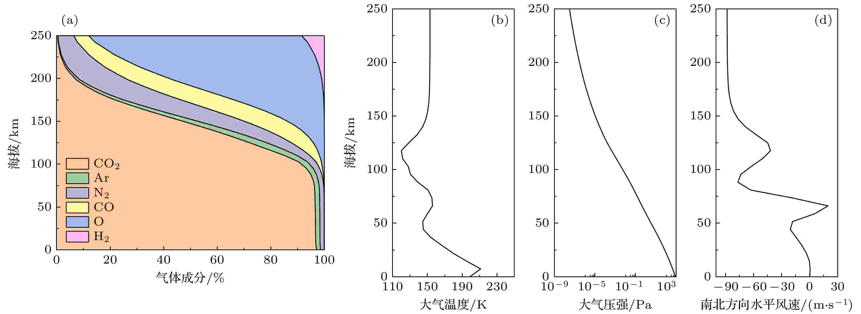
At present, Mars acoustic detection is gradually becoming an important new tool for understanding and exploring Mars. To explore the sources of Mars sound, it is necessary to study the sound speed and the sound attenuation in the thin and low-temperature Martian atmosphere, and to model the sound propagation in the stratified atmosphere. According to the extremely low pressure of Mars and the large variation of gas composition with altitude, we propose a simulation method based on the Navier-Stokes (NS) equation and the mixed-gas model to calculate the vertical profiles of sound speed and attenuation in the Martian atmosphere at 0–250 km altitude in this work. A comparison among sound-speed profiles at different frequencies shows that there is a notable sound dispersion in the Martian atmosphere, especially at high altitudes and in the high frequency range. It is also verified through sound speed measurement experiments that significant sound dispersion does exist in low-pressure carbon dioxide, implying the need to consider sound dispersion in the modelling of Martian sound speed profiles. The scope of application of the NS equation in modelling the sound speed of the Martian atmosphere is also discussed, as the NS equation may fail in a too rarefied gas. Next, the non-dispersive ideal-gas sound speed profiles and the dispersive NS sound speed at different frequencies (0.01, 0.1, 1 Hz) are used to simulate the sound propagation paths in the multilayered Martian atmosphere. And both cases of the Martian ground-based and high-altitude sources are compared with each other. It is found that the dispersive sound speed has a significant effect on the sound propagation path on Mars. The main influence is that the first fold back height and the first return distance of the sound ray to the surface are both shortened, which directly changes the area and location of the acoustic quiet zone. The effect of dispersion on the sound propagation path becomes more notable with both the frequency and the elevation of the acoustic source increasing, confirming that consideration of dispersion has a significant effect on the calculation of the sound propagation path.
2022, 71 (24): 244601.
doi: 10.7498/aps.71.20221340
Abstract +
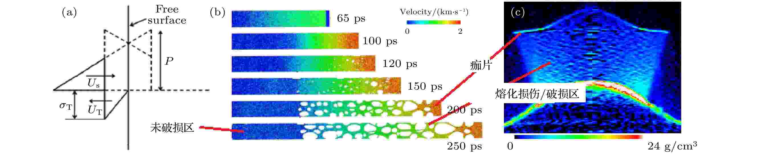
A strong shock-wave, produced by plate impact, explosive detonation or laser irradiation, can induce metal materials to melt. Reflection of the triangular pressure wave from the free surface generates a strong tensile stress in the liquid state, resulting in the creation of an expanding cloud of liquid debris. This phenomenon is called micro-spalling. The understanding of spall damage evolution and dynamic fragmentation of melted metal under shockwave loading and subsequent releasing is an issue of considerable importance for both basic and applied science, to predict the evolution of engineering structures subjected to explosive detonation in implosive dynamics or inertial confinement fusion, the latter involving high energy laser irradiation of thin metallic shells. For dynamic failure processes, spall fracture in solid material has been extensively studied for many years, while scarce data can be found about how such a phenomenon can evolve after being melted partially or fully when being compressed or released. In this paper, by studying the physical laws of void evolution in melted metals, we expect to reveal the mode and criterion of void coalescence, inertial and temperature effects on void distribution and evolution, and the relationship between fragment distribution and characteristics of breakup of damaged material. According to these physical laws, we can develop theoretical model to describe the damage evolution and fragment distribution of metal that melts when shock releases. This model is implemented as a failure criterion in a one-dimensional hydrocode. The experimental results and computational results are in fairly good agreement with each other. Some discrepancies are explained by using both experimental uncertainties and model limitations which are carefully pointed out and discussed. We believe that these results can deepen our physical understanding of the damage evolutions of metals and improve the credibility of numerical simulation on the damage and fragmentation of materials under implosive loading.
PHYSICS OF GASES, PLASMAS, AND ELECTRIC DISCHARGES
2022, 71 (24): 245201.
doi: 10.7498/aps.71.20221555
Abstract +
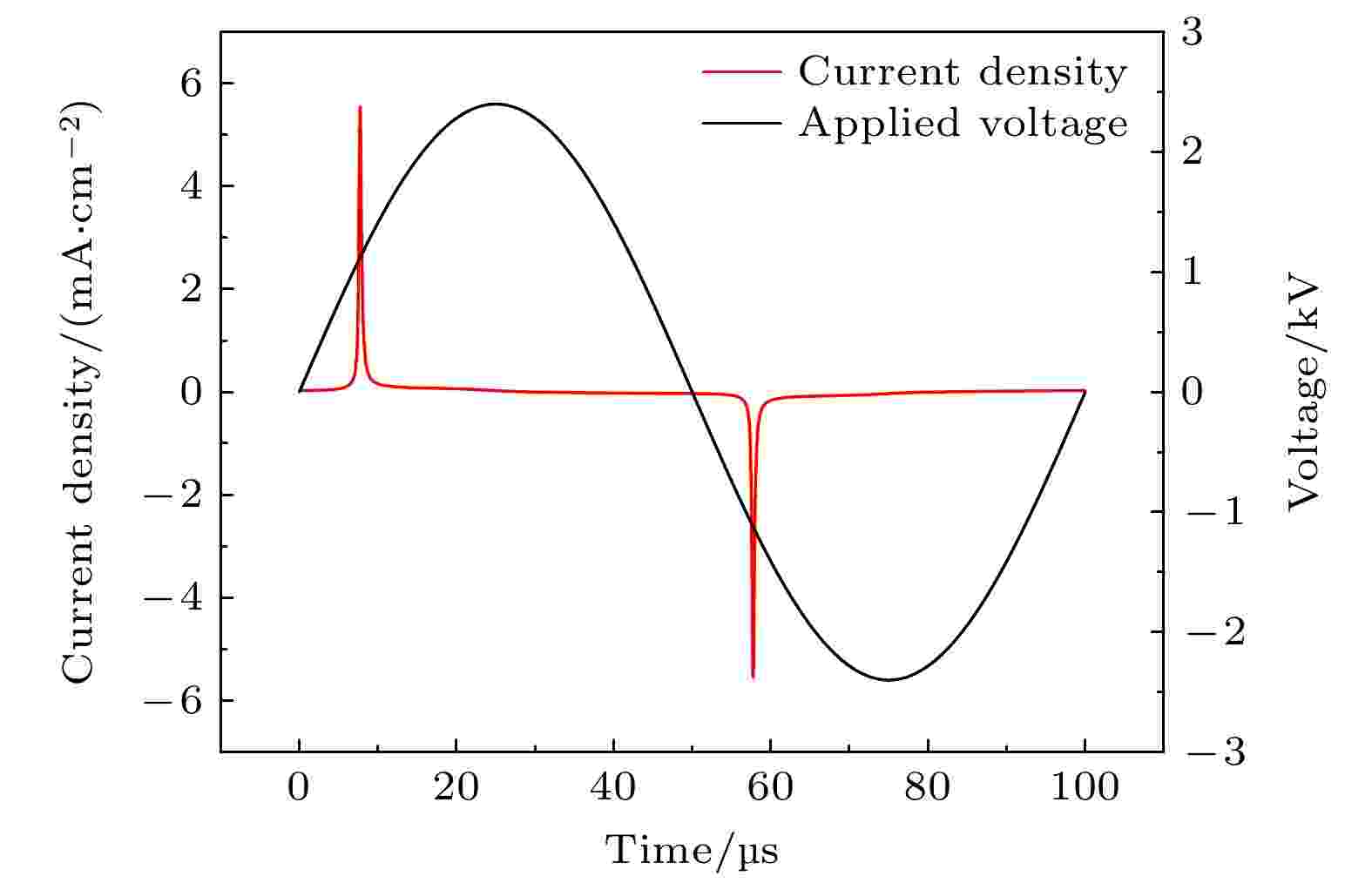
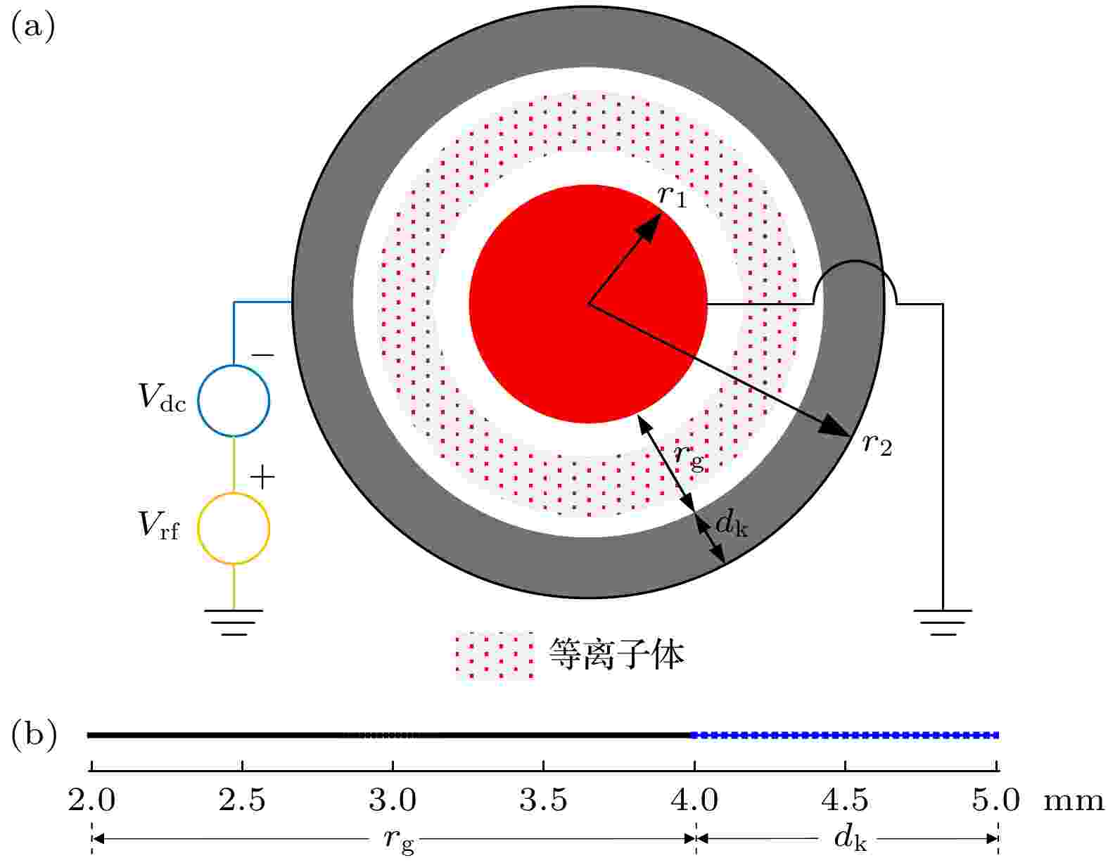
In recent years, with the development of gas discharge technology at atmospheric pressure, the application of low temperature plasma has received widespread attention in pollution prevention, disinfection, sterilization, energy conversion and other fields. Atmospheric dielectric barrier discharge is widely used to produce low temperature plasma in various applications, which is usually numerically investigated by using fluid models. The unique advantages of machine learning in various branches of physics have been discovered with the advancement of big data processing technology. Recent studies have shown that artificial neural networks with multiple hidden layers have a pivotal role in the simulation of complex datasets. In this work, a fully connected multilayer BP (back propagation) network together with a universal hidden layer structure is developed to explore the characteristics of one or more current pulses per half voltage cycle of atmospheric dielectric barrier discharge. The calculated data are used as training sets, and the discharge characteristics such as current density, electron density, ion density, and electric field of atmospheric dielectric barrier discharge can be quickly predicted by using artificial neural network program. The computational results show that for a given training set, the constructed machine learning program can describe the properties of atmospheric dielectric barrier discharge with almost the same accuracy as the fluid model. Also, the computational efficiency of the machine learning is much higher than that of the fluid model. In addition, the use of machine learning programs can also greatly extend the calculation range of parameters. Limiting discharge parameter range is considered as a major challenge for numerical calculation. By substituting a relatively limited set of training data obtained from the fluid model into the machine learning, the discharge characteristics can be accurately predicted within a given range of discharge parameters, leading an almost infinite set of data to be generated, which is of great significance for studying the influence of discharge parameters on discharge evolution. The examples in this paper show that the combination of machine learning and fluid models can greatly improve the computational efficiency, which can enhance the understanding of discharge plasmas.
2022, 71 (24): 245202.
doi: 10.7498/aps.71.20221361
Abstract +
COVER ARTICLE
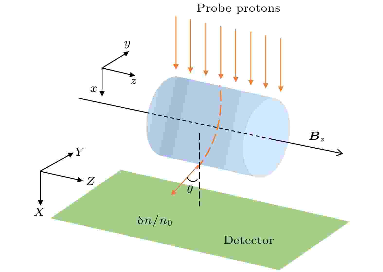
2022, 71 (24): 245203.
doi: 10.7498/aps.71.20221848
Abstract +
The magnetic fields generated in plasmas have extensive influences on many processes of the inertial confinement fusion and the astrophysics. Therefore, the quantitative diagnosis of the magnetic field is quite essential. Proton radiography is a widely used experimental technique to diagnose the electric field or magnetic field in high-energy-density plasma. The effective explanation of the results of proton radiography depends on the reliability and availability of the inversion method. Traditional inversion methods can only provide one- or two-dimensional structure of the self-generated magnetic field. In this study, it is found that there is an Abel transformation relationship between the deflection velocity and the magnetic field with column symmetry, which allows us to reconstruct the three-dimensional structure of the magnetic field for the first time. We theoretically deduce the process of reconstructing the cylindrical magnetic field through proton radiography with the Abel inversion algorithm. The feasibility of this method is verified by numerical simulation as well. Based on this inversion method, we reanalyze the proton radiography experimental results of Li et al. (2016 Nat. Commun. 7 13081 ) on the self-generated magnetic field of plasma jets. The inversion results show that the maximum magnetic field intensity is about 1.9 times the traditional inversion results. We discuss a new proton radiography inversion method for the existence of magnetic fields with cylindrical symmetry in thiswork, which will contributes to an intensive understanding of the self-generated electromagnetic field and its spatiotemporal evolution related to the laser fusion and the laboratory astrophysics.
CONDENSED MATTER: STRUCTURAL, MECHANICAL, AND THERMAL PROPERTIES
2022, 71 (24): 246101.
doi: 10.7498/aps.71.20221621
Abstract +
High-entropy alloys have broad application prospects in aviation, aerospace, military and other fields due to their excellent mechanical properties. Temperature is an important external factor affecting the shock response of high-entropy alloys. In this paper, we investigate the effects of temperature on the shock response and plastic deformation mechanism of CoCrFeMnNi high-entropy alloys by using molecular dynamics method. The effects of temperature on the atomic volume and the radial distribution function of CoCrFeMnNi high-entropy alloy are studied. Then, the piston method is used to generate shock waves in the sample to study the shock response of CoCrFeMnNi high-entropy alloy. We observe the evolution of atomic-scale defects during the shock compression by the polyhedral template matching method. The results show that the shock pressure, the shock wave propagation velocity, and the rising of shock-induced temperature all decrease with the initial temperature increasing. For example, when piston velocity Up = 1.5 km/s, the shock pressure at an initial temperature of 1000 K decreases by 6.7% in comparison with that at 1 K. Moreover, the shock Hugoniot elastic limit decreases linearly with the increase of temperature. The Hugoniot Up-Us curve of CoCrFeMnNi HEA in the plastic stage can be linearly fitted by the formula Us = c0 + sUp, where c0 decreases with temperature increasing. As the shock intensity increases, the CoCrFeMnNi high-entropy alloy undergoes complex plastic deformation, including dislocation slip, phase transformation, deformation twinning, and shock-induced amorphization. At relatively high initial temperature, disordered clusters appear inside CoCrFeMnNi HEA, which together with the BCC (body-centered cubic) structure transformed from FCC (face-centered cubic) and disordered structure are significant dislocation nucleation sources. Compared with other elements, Mn element accounts for the largest proportion (25.4%) in disordered cluster. Owing to the large atomic volume and potential energy, large lattice distortion and local stress occur around the Mn-rich element, which makes a dominant contribution to shock-induced plastic deformation. At high temperatures, the contribution of Fe element to plastic deformation is as important as that of Mn element. The research results are conducive to understanding the shock-induced plasticity and deformation mechanisms of CoCrFeMnNi high-entropy alloys in depth.
2022, 71 (24): 246102.
doi: 10.7498/aps.71.20221847
Abstract +
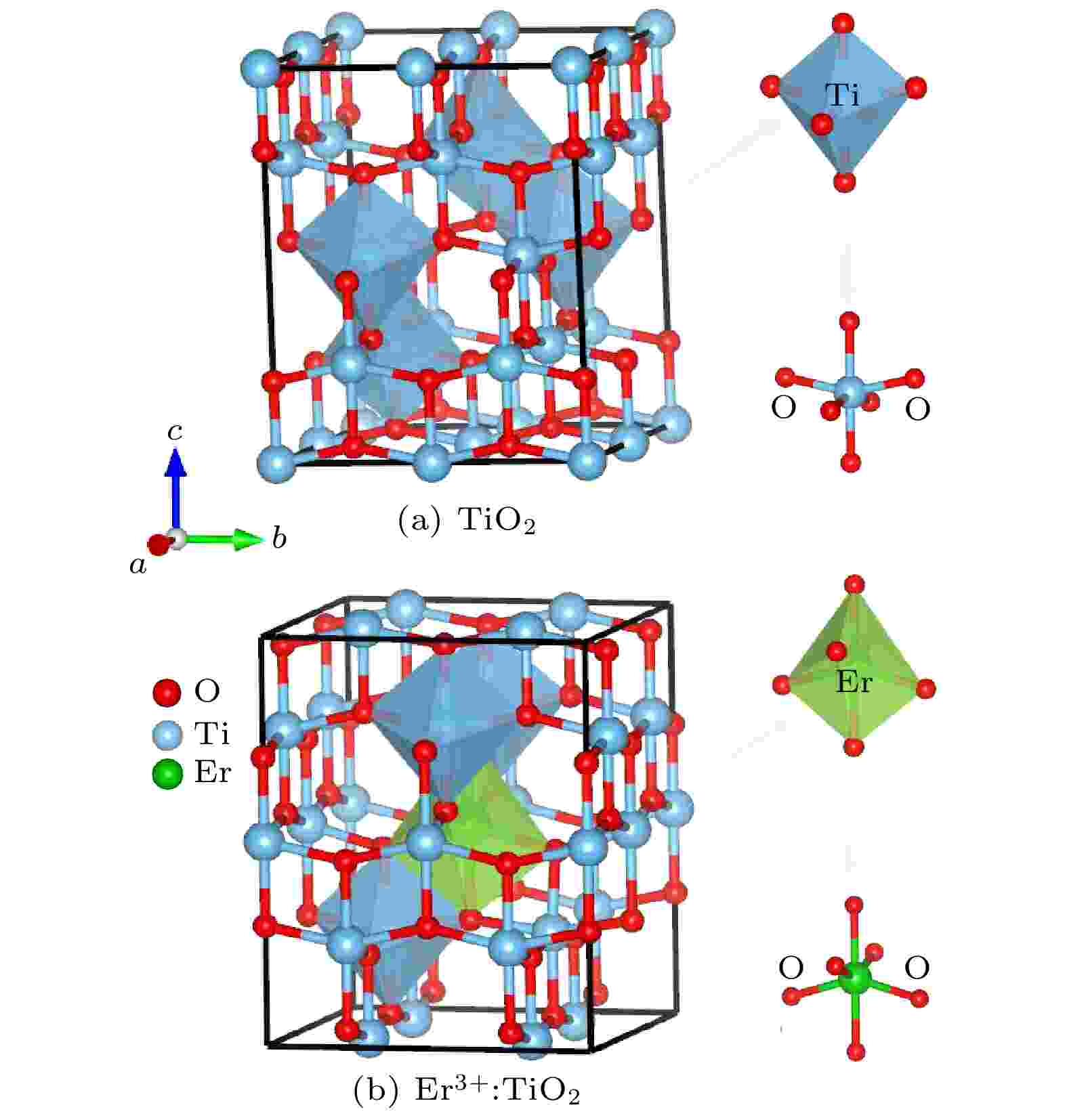
Trivalent rare earth erbium ion (Er3+) doped titanium oxide (TiO2) can possess a very wide range of applications due to its excellent optoelectronic properties, thus standing out among many rare-earth-doped luminescent crystals. However, the issues regarding local structure and electronic properties have not been finalized. To address these problems, the CALYPSO (Crystal structure AnaLYsis by Particle Swarm Optimization) method combined with the first-principles calculations is employed, and many converged structures of Er3+-doped TiO2 are successfully obtained. Further structural optimization is performed by using the VASP (Vienna ab initio simulation package) software package, and we report for the first time that the lowest energy structure of Er3+-doped TiO2 has the $ P\overline 4 $ m2 symmetry. It can be observed that the doped Er3+ ions enter into the host crystal and occupy the positions of Ti4+ ions, resulting in structural distortion, which eventually leads the local Er3+ coordination site symmetry to reduce from D2d into C2v. We speculate that there are two reasons: 1) the difference in charge between Er3+ ions and Ti4+ ions leads to charge compensation; 2) the difference between their electron radii is obvious: the radius is 0.0881 for Er3+ ion and 0.0881 for Ti4+ ion. In addition, during the structural search, we also find many metastable structures that may exist at a special temperature or pressure, which play an important role in the studying of structural evolution. When the electronic band structure of the Er3+-doped TiO2 system is calculated, we adopt the method of local density approximation (LDA) combined with the on-site Coulomb repulsion parameter U to accurately describe the strongly correlated system. For the specific value of U, we adopt 3.5 eV and 7.6 eV to describe the strong correlation of 3d electrons of Ti4+ ions and 4f electrons of Er3+ ions, respectively. According to the calculation of electronic properties, the band gap value of Er3+ doped TiO2 is about 2.27 eV, which is lower than that of the host crystal (Eg = 2.40 eV). The results show that the reduction in the band gap is mainly caused by the f state of Er3+ ions. The doping of Er ion does reduce the band gap value, but it does not change the conductivity of the system, which have great application prospect in diode-pumped laser. These findings not only provide the data for further exploring the properties and applications of Er3+:TiO2 crystals, but also present an approach to studying other rare-earth-doped crystalline materials.

CONDENSED MATTER: ELECTRONIC STRUCTURE, ELECTRICAL, MAGNETIC, AND OPTICAL PROPERTIES
2022, 71 (24): 247301.
doi: 10.7498/aps.71.20221365
Abstract +
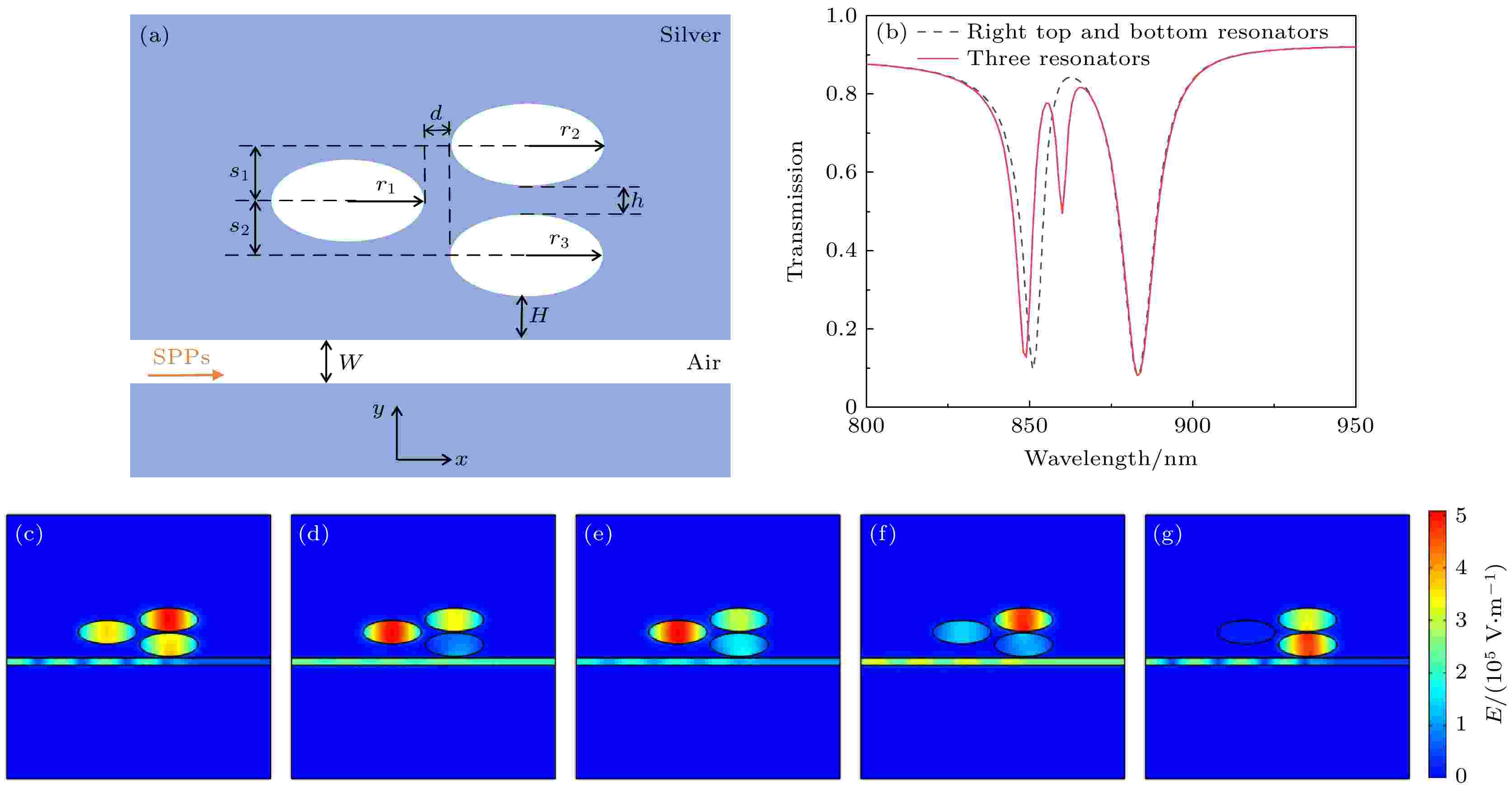
The tunable double plasmon-induced transparency (PIT) effects are investigated in a waveguide coupled by the three ellipse-shaped resonators. By the finite element method, we study the influences of coupling modes of the three ellipse-shaped resonators, waveguide structure parameters and the refractive indices of dielectric in three ellipse-shaped resonators on double PIT effects. The waveguide structure consists of three ellipse-shaped resonators, and is similar to a four-level structure of the atomic system. The bottom ellipse-shaped resonator can be named a bright mode, the middle and top ellipse-shaped resonators each can be seen as a dark mode. In order to obtain an ideal double PIT transparency window, we also numerically analyze the optical transmission characteristics of structures of several three-ellipse-shaped resonator coupled waveguides. Furthermore, we mainly discuss the transmission spectra in the better three-ellipse-shaped resonator coupled waveguide structure as a function of the radii of the long axis in ellipse-shaped resonators, the coupling distance between the bottom ellipse-shaped resonator and the bus waveguide, the coupling distance between ellipse-shaped resonators, and the symmetry broken degree. In addition, we also consider the effect of the refractive indices of dielectric in three ellipse-shaped resonators on double PIT spectra. It is found that the transmission spectra in the three-ellipse-shaped resonator coupled waveguide have obvious red shift when the refractive indices of dielectric in the three ellipse-shaped resonators increase. All the simulation results may provide the theoretical basis for the potential application of multiple PIT in plasma switches and sensors.
EDITOR'S SUGGESTION
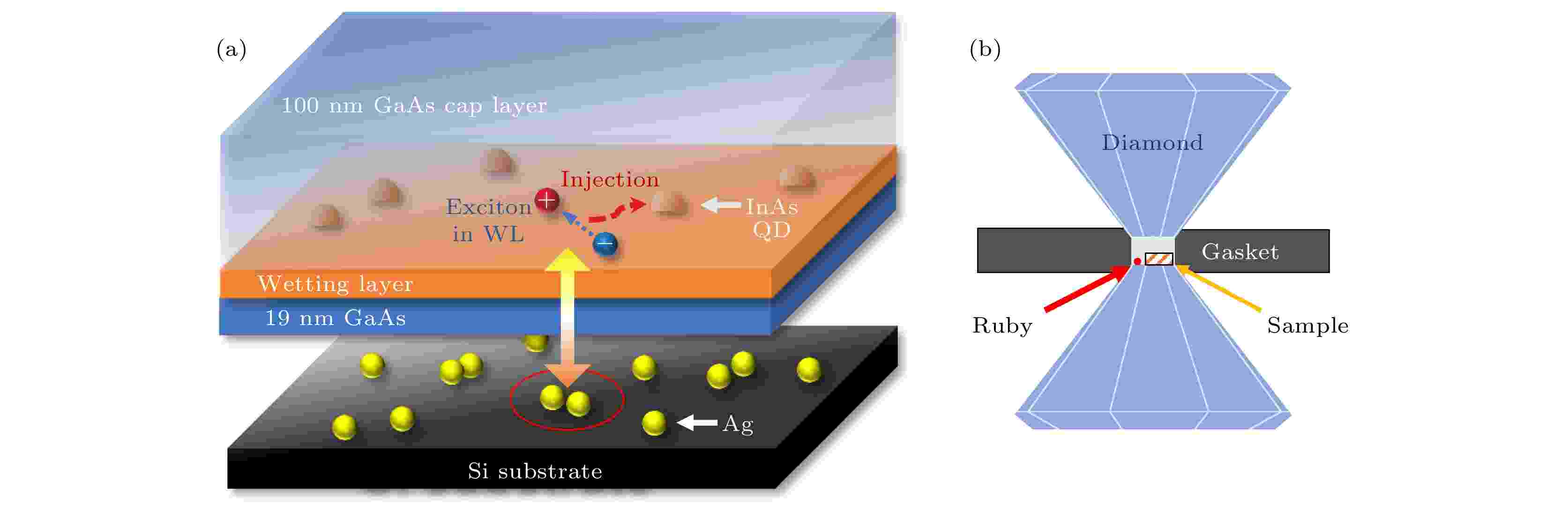
2022, 71 (24): 247302.
doi: 10.7498/aps.71.20221344
Abstract +
In the past few decades, the studies of exciton emissions coupled with the metal nanoparticles have mainly focused on the enhancing exciton radiation and reducing exciton lifetime by near-field coupling interactions between excitons and metal nanoparticles. Only in recent years has the plasmon-field-induced to extend exciton lifetime (inhibition of the exciton emission) been reported. Experimentally, for observing a long-lifetime exciton state it needs to satisfy a condition of $kz\sim1$ , instead of near-field condition of $ kz\ll 1 $ , where $k=2{\pi }n/\lambda$ is the wavevector, $ n $ is the refractive index, $ \lambda $ is the wavelength, and $ z $ is the separation distance between the emitter and metal nanoparticle. Thus, in this paper, we tune the exciton emission wavelength by applying hydrostatic pressure to achieve the condition of $kz\sim1$ in order to in detail investigate the coupling between excitons and metal nanoparticles. The studied InAs/GaAs quantum dot (QD) sample is grown by molecular beam epitaxy on a (001) semi-insulating GaAs substrate. After the AlAs sacrificial layer is etched with hydrofluoric acid, the QD film sample is transferred onto an Si substrate covered with Ag nanoparticles. Then the sample is placed in the diamond anvil cell device combined with a piezoelectric ceramic. In this case we can measure the photoluminescence and time-resolved photoluminescence spectra of the QD sample under different pressures. It is found that the observed longest exciton lifetime is $(120\pm 4)\times 10~\rm{n}\rm{s}$ at a pressure of $ 1.38\;\rm{G}\rm{P}\rm{a} $ , corresponding the exciton emission wavelength of $ 797.49\;\rm{n}\rm{m} $ , which is about $ 1200 $ times longer than the exciton lifetime of $\sim 1\;\rm{n}\rm{s} $ in QDs without the influence of Ag nanoparticles. The experimental results can be understood based on the destructive interference between the quantum dot exciton radiation field and the scattering field of metal nanoparticles. This model proposes a convenient way to increase the emission lifetime of dipoles on a large scale, and is expected to be applied to quantum information processing, optoelectronic applications, fundamental physics researches such as Bose-Einstein condensates.


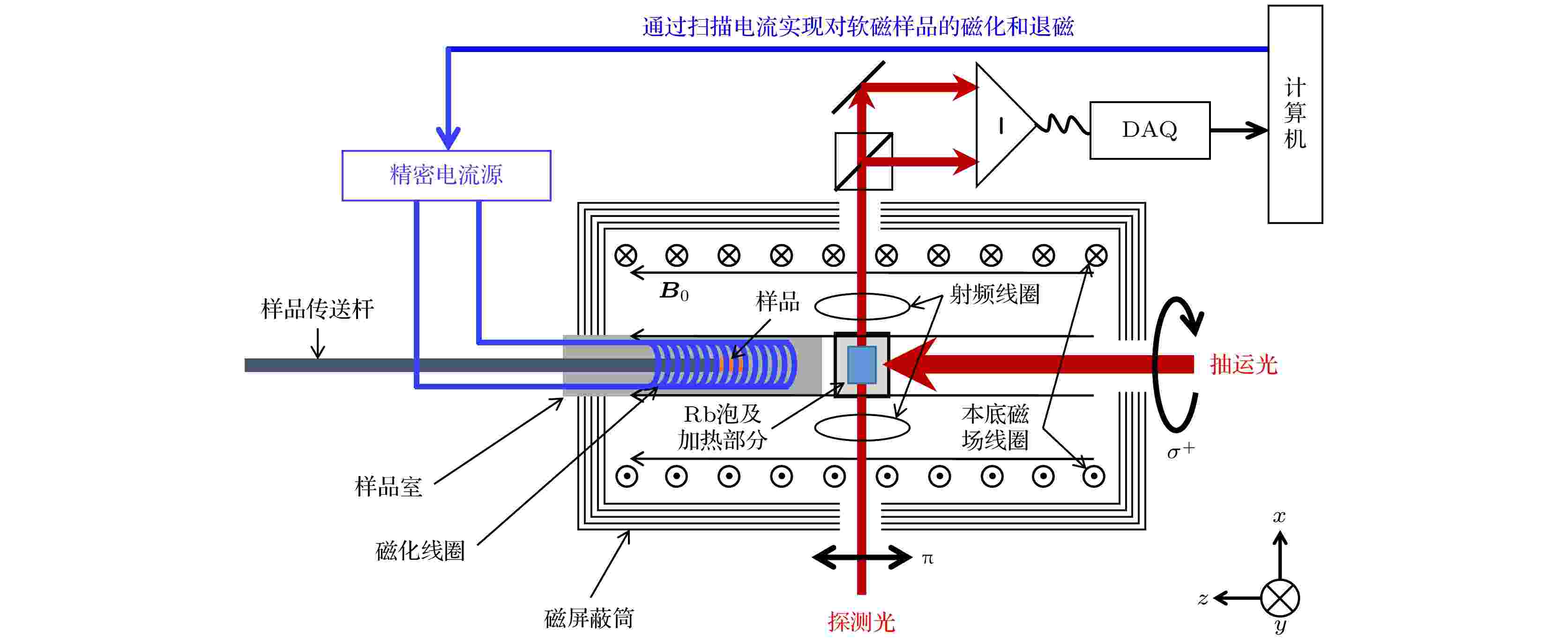
2022, 71 (24): 247501.
doi: 10.7498/aps.71.20221509
Abstract +
Fe-based amorphous and nanocrystalline soft magnetic alloys are regarded as the significant dual-green energy-saving materials because of their superior magnetic properties and straightforward fabrication procedure. As such, they have attracted much attention in the fields of the electronic information and electrical power. In this work, Fe73.5Cu1Nb3Si13.5B9 (%) amorphous alloy ribbon is subjected to various physical ageing treatments in nitrogen atmosphere. These treatments include annealing at 540 ℃ for 30 min under different tensile stresses and isothermal tempering without tensile stress for several cycles. The origin of stress-induced magnetic anisotropy is investigated through using dynamic strain analysis, the longitudinally driven giant magento-impedance effect, and synchrotron radiation X-ray diffraction. In the process of tensile stress annealing, it is found that the axial strain of ribbon is elastic strain when annealing temperature is below the glass transition point, and plastic strain when annealing temperature is above the glass transition point; the precipitation of nanocrystalline phase has a pinning effect on amorphous matrix, which slows down the strain rates and makes the tend stable. Additionally, isothermal tempering studies show that the stress-induced magnetic anisotropy and lattice plane anisotropy have different relaxation patterns. It is found through numerical fitting that the stress-induced magnetic anisotropy can reach a stable value of 0.144 by infinite tempering, whereas the lattice plane anisotropy can only relax to zero by finite tempering. A model of nanocrystalline grain distribution anisotropy is developed to re-examine the origin of stress-induced magnetic anisotropy. It supports a viewpoint that the nanocrystalline grain distribution anisotropy $\Delta \delta $ is responsible for the stress-induced irreversible magnetic anisotropy ${K_{\text{d}}}$ , and that their relationship can be described as a following function: ${K_{\text{d}}} = k\Delta \delta $ . Therefore, it is proposed that the stress-induced anisotropy originates from a synergistic interaction between the lattice plane anisotropy and the nanocrystalline grain distribution anisotropy in Fe-based alloy ribbon. This work has important implications for understanding the mechanism of the stress-induced magnetic anisotropy.


2022, 71 (24): 247502.
doi: 10.7498/aps.71.20220591
Abstract +
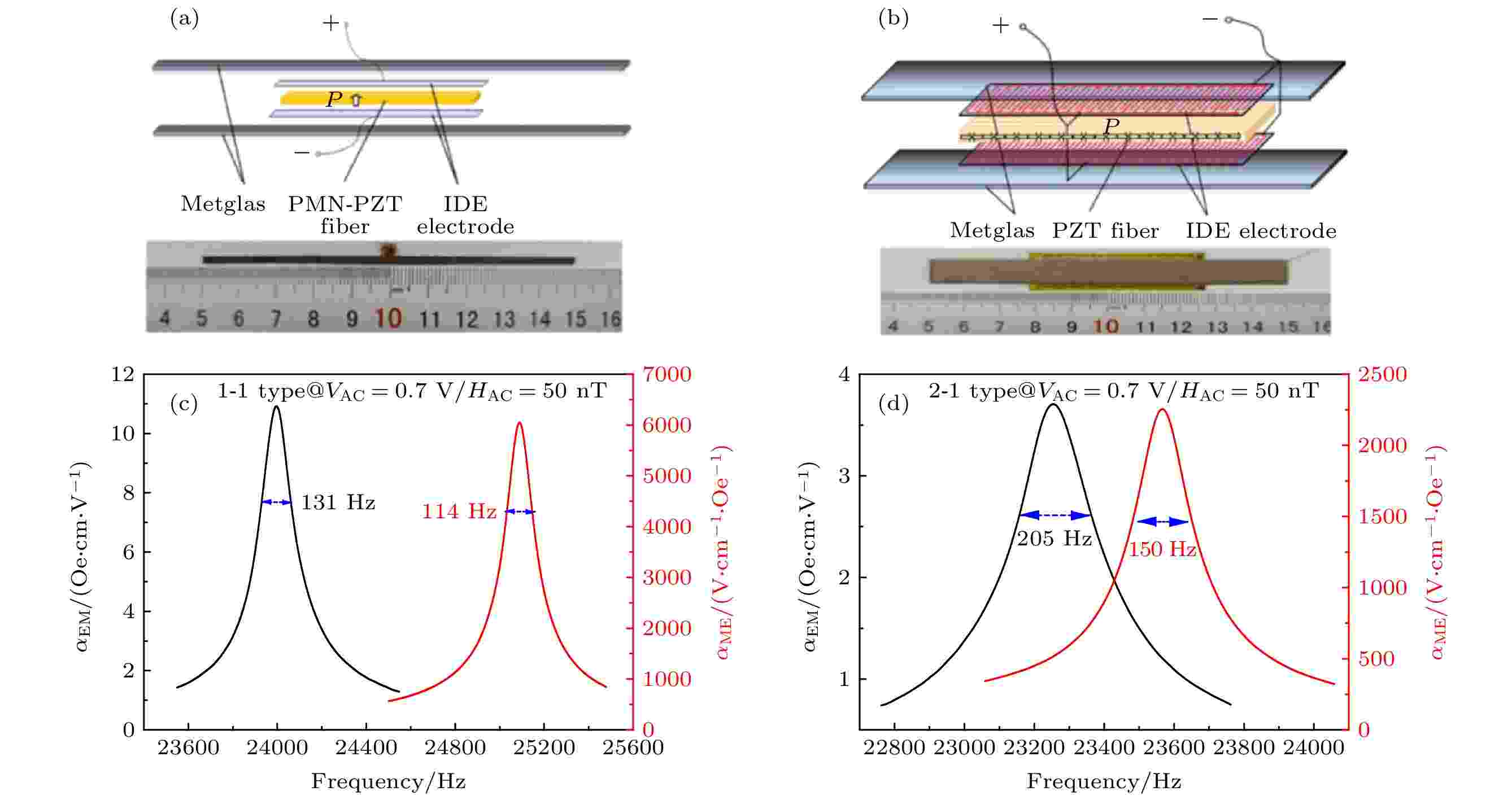
Mechanical antenna, a novel scheme for realizing very low frequency (VLF) and portable transmitters, has been investigated recently. In this work, the impedance characteristics of 1-1 type of and 2-1 type of magnetoelectric (ME) mechanical antennas are systematically studied and compared with each other. Based on the measured frequency-impedance curves and the corresponding modified Butterworth-van Dyke (MBVD) model, three characteristic frequency points, i.e. the minimum impedance frequency $ {f}_{\rm{m}} $ , the series resonance frequency $ {f}_{\rm{s}} $ , and the resonance frequency $ {f}_{\rm{r}} $ are obtained and discussed. On this basis, the influence of driving voltage, bias magnetic field, and the quality factor (Q value) on ME antenna impedance characteristics are experimentally explored. Finally, the reactance components of both 1-1 type of and 2-1 type of ME antenna are collected by referring to the actual working frequency $ {f}_{\rm{d}} $ . Experimental results prove that the resonant ME antennas are basically pure resistive vibrators, while an ME antenna with high Q value normally fails to support high driving field because of the low resistance (< 100 Ω) and the strong nonlinearity. Thus, the field radiation capability in 2-1 type of ME antenna is higher than that in 1-1 typed one. This work provides the ideas for choosing Q value and further optimizing a magnetoelectric antenna based on the understanding of its impedance characteristics.


EDITOR'S SUGGESTION
2022, 71 (24): 247801.
doi: 10.7498/aps.71.20221417
Abstract +
2022, 71 (24): 247803.
doi: 10.7498/aps.71.20221002
Abstract +
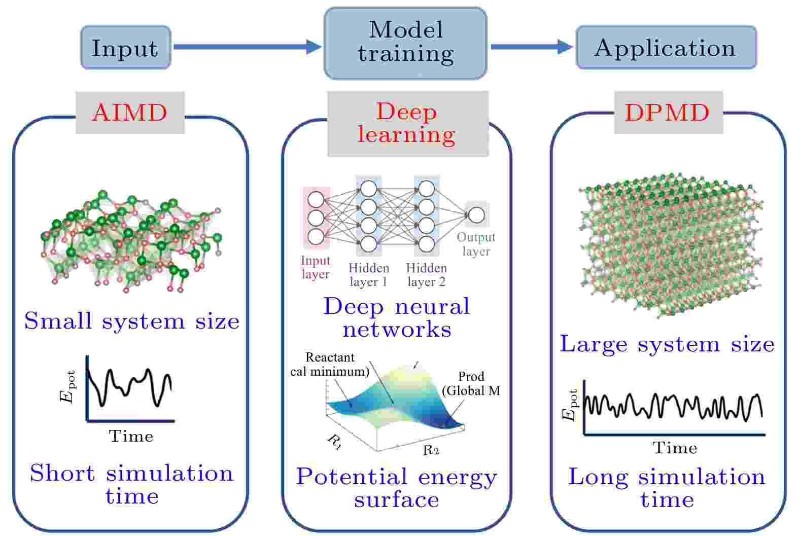
Silicon nitride (β-Si3N4) is a most promising thermal wave-transparent material. The accurate measurement of its high-temperature dielectric function is essential to solving the “black barrier” problem of hypersonic vehicles and accelerating the design of silicon nitride-based thermal wave-transparent materials. Direct experimental measurement at high temperature is a difficult job and the accuracy of classical molecular dynamics (CMD) simulations suffers the choice of empirical potential. In this work, we build a β-Si3N4 model on a nanoscale, train the deep learning potential (DLP) by using first-principles data, and apply the deep potential molecular dynamics (DPMD) to simulate the polarization relaxation process. The predicted energy and force by DLP are excellently consistent with first-principles calculations, which proves the high accuracy of DLP. The RMSEs for β-Si3N4 are quite low (0.00550 meV/atom for energy and 7.800 meV/Å for force). According to the Cole-Cole formula, the microwave dielectric function in the temperature range of 300–1000 K is calculated by using the deep learning molecular dynamics method. Compared with the empirical potential, the computational results of the DLP are consistent with the experimental results in the sense of order of magnitude. It is also found that the DPMD performs well in terms of computational speed. In addition, a mathematical model of the temperature dependence of the relaxation time is established to reveal the pattern of relaxation time varying with temperature. The high-temperature microwave dielectric function of silicon nitride is calculated by implementing large-scale and high-precision molecular dynamics simulations. It provides fundamental data for promoting the application of silicon nitride in high-temperature thermal transmission.
2022, 71 (24): 247901.
doi: 10.7498/aps.71.20221496
Abstract +
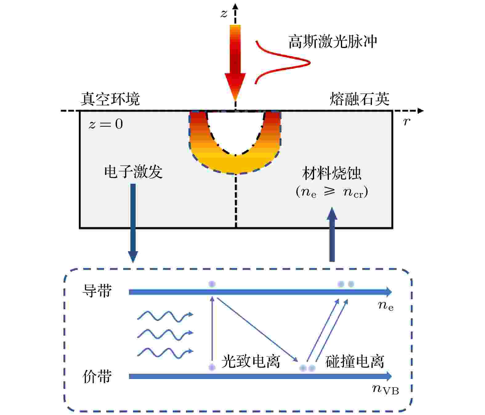
The ablation threshold, depth and crater shape of fused silica for femtosecond laser processing are investigated theoretically and experimentally. Based on tracking the spatiotemporal distribution of the free electron density, free electron temperature, and laser intensity, the electron dynamics as well as the transient optical and thermophysical properties of femtosecond laser irradiated fused silica are quantitatively determined. The numerical model is validated by comparing the calculated threshold fluence, depth and crater shape of ablation with the experimentally measured ones at a wavelength of 800 nm. The free electron relaxation time at different laser fluences and pulse durations throughout the photoionization process and impact ionization process are probed. In the present work, the findings are as follows. 1) The electron relaxation time significantly affects the material optical properties and femtosecond laser energy absorption. The optical properties change dramatically. The fused silica becomes opaque for the case of laser irradiation with fluence higher than the ablation threshold. Moreover, the transition from electron-phonon collision to electron-ion collision accompanies with the femtosecond laser ablation of fused silica. 2) By using the proposed model, the experimentally observed saturation of ablation depth at high laser fluence is elucidated by the significant change of optical reflectivity and absorption coefficient. Both the results of theoretical simulation and experimental observation indicate that laser fluence has a strong influence on the shape of the ablation crater. The ablation volume increases sharply with the increase of laser fluence for femtosecond laser irradiation, compared with that for picosecond laser irradiation. 3) With the increase of femtosecond laser fluence, the ablation depth removal efficiency and ablation efficiency are both saturated, followed by slight decrements. The peak of ablation depth removal efficiency peak occurs at the femtosecond laser fluence close to 1.4 times of the ablation threshold. While the accuracy is slightly low due to the higher sensitivity of the ablation characteristics (ablation crater depth and ablation volume) to the shorter femtosecond laser pulse. For the femtosecond laser fluence higher than 3.5 times of the ablation threshold, good repeatability over a very wide fluence range can achieve accurate processing results, because a more consistent flat-bottom ablation profile tends to appear. However, the heat-affected zone leads the processing quality to degrade, compared with the scenario of femtosecond laser fluence close to the ablation threshold.
INTERDISCIPLINARY PHYSICS AND RELATED AREAS OF SCIENCE AND TECHNOLOGY
2022, 71 (24): 248201.
doi: 10.7498/aps.71.20221294
Abstract +
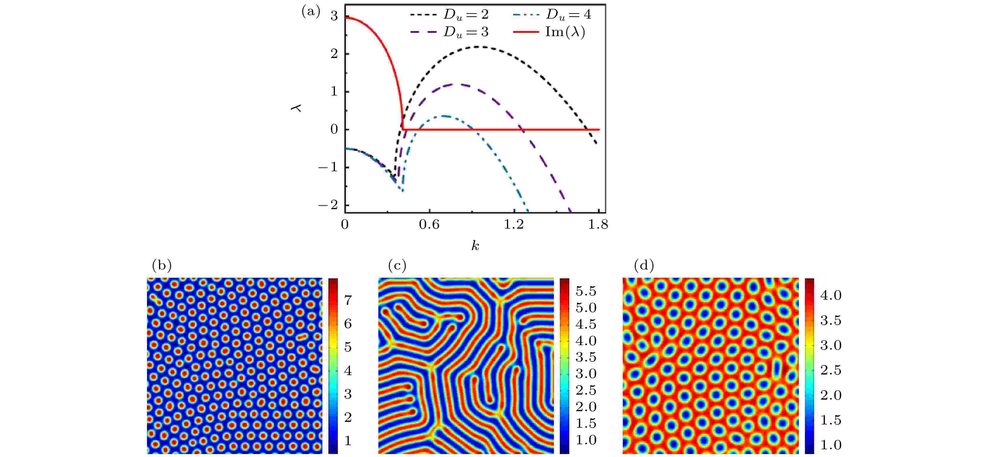
Diffusion plays a crucial role in the forming and evolving of Turing patterns. Generally, the diffusion processes in complex systems do not comply to the complete random walk theory, which means that the diffusion is abnormal rather than normal, such as super-diffusion, sub-diffusion and anisotropic diffusion. However, most of previous studies focused on the pattern formation mechanism under the normal diffusion. In this paper, a two-component reaction-diffusion model with anisotropic diffusion is used to study the effect of anisotropic diffusion on Turing patterns in heterogeneous environments. Three different types of anisotropic diffusions are utilized. It is shown that the system gives rise to stripe patterns when the degree of anisotropic diffusion is high. The directions of stripes are determined by the degree of the diffusion coefficient deviating from the bifurcation point. In a low degree of anisotropic diffusion, the pattern type is the same as the counterpart in a low degree of the isotropic diffusion. When the diffusion coefficient grows linearly in the space, different types of patterns compete with each other and survive in different regions under the influence of spatial heterogeneity. When the diffusion coefficient is modulated by a one-dimensional periodic function, both type and wavelength of the pattern are determined by the modulated wavelength and the intrinsic wavelength. The system can exhibit alternating two-scale mixed patterns of different types when the modulated wavelength is larger than the intrinsic wavelength. Note that each of the diffusion coefficients of some special anisotropic media is a tensor, which can be expressed as a matrix in two-dimensional cases. We also study the influence of off-diagonal diffusion coefficient D on Turing pattern. It is found that the Turing pattern induced by off-diagonal diffusion coefficient always selects the oblique stripe pattern. The off-diagonal diffusion coefficient D not only affects the pattern selection mechanism, but also expands the parameter range of Turing space. The critical diffusion coefficient $ {D_{\text{c}}} $ increases linearly with the diagonal diffusion coefficient $ {D_u} $ increasing. The intrinsic wavelength of the oblique stripe pattern decreases as the off-diagonal diffusion coefficient D increases. It is interesting to note that the critical wavelength corresponding to the critical diffusion coefficient $ {D_{\text{c}}} $ is independent of the diagonal diffusion coefficient $ {D_u} $ . These results not only provide a new insight into the formation mechanism of Turing patterns, but also increase the range and complexity of possible patterns.


Effect of Sb/Bi atom substitution site on electronic transport properties of Mg2Si0.375Sn0.625 alloy
2022, 71 (24): 248401.
doi: 10.7498/aps.71.20221364
Abstract +
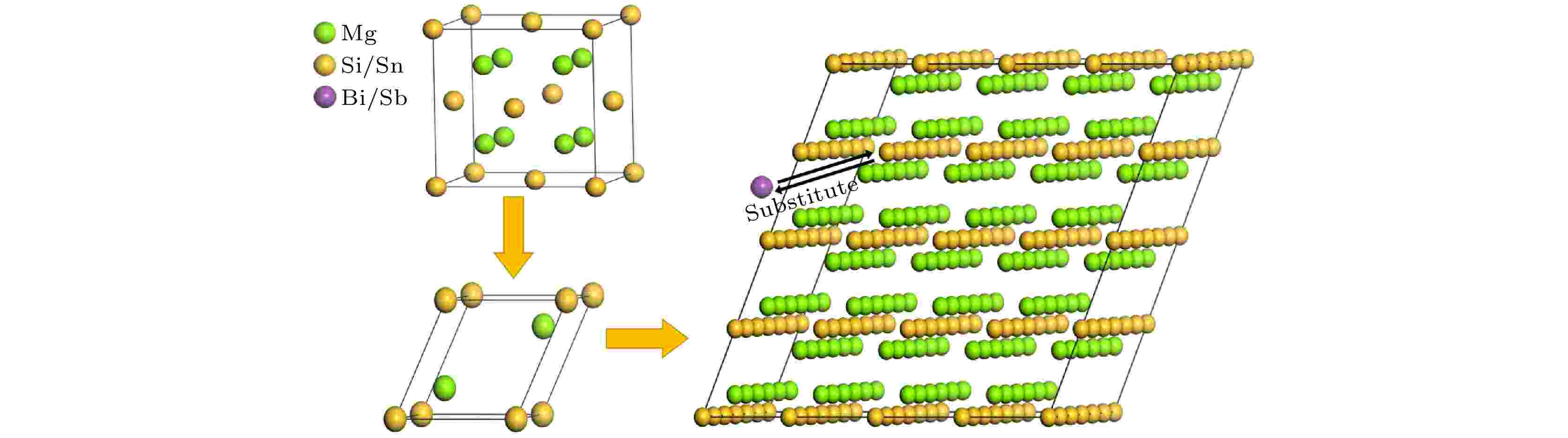
Mg2(Si,Sn)-based thermoelectric materials, which are environmentally friendly and low-cost, have great development potential in a moderate temperature range. Electronic transport properties of Mg2Si1-xSnx alloys can be optimized by doping elements. Doping is still one of the most effective methods of optimizing electronic transport performance, such as carrier concentration, mobility, and effective mass. The most effective doping elements are Sb and Bi. Much attention has been paid to the influence of element type and doping content. Different substitution sites will also greatly affect the electronic transport parameters. In this work, the defect formation energy value of Mg2Si0.375Sn0.625 alloy for substituting Sb atoms and Bi atoms for Sn sties and Si sites, respectively, are calculated by first-principles calculations. The influence on electronic transport parameters is systematically analyzed by combining the calculated results of band structures and density of states. Corresponding component Sb and Bi atoms doped Mg2Si0.375Sn0.625 alloys are prepared by rapid solidification method, and microstructures, Seebeck coefficients, and electrical conductivities of the alloys are measured. Combined with the predicted results by solving the Boltzmann transport equation, electronic transport performances are compared and analyzed. The results indicate that both Sn and Si sites are equally susceptible to Sb and Bi doping, but the Si sites are preferentially substituted due to their lower ∆Ef values. Doped Bi atoms provide a higher electron concentration, and Sb atoms offer higher carrier effective mass. Thus, the maximum σ value of the Mg2Si0.375Sn0.615Bi0.01 alloy is 1620 S/cm. The maximum S value of the Mg2Si0.365Sn0.625Sb0.01 alloy is –228 μV/K. Correspondingly, the highest PF value for this alloy is 4.49 mW/(m·K) at T = 800 K because of the dominant role of S values. Although its power factor is slightly lower, the Mg2Si0.375Sn0.615Sb0.01 alloy is expected to exhibit lower lattice thermal conductivity due to the lattice shrinkage caused by substituting Sb sites for Sn sites. The optimal doping concentration of the Bi-doped alloy is lower than that of the Sb-doped alloy. These results are expected to provide a significant reference for optimizing the experimental performance of Mg2(Si, Sn)-based alloys.
2022, 71 (24): 248402.
doi: 10.7498/aps.71.20221503
Abstract +
In this paper, a 360° continuously scanning circular array antenna is presented. The circular array consists of eight Yagi-Uda monopoles, each one consisting of a driver, a reflector and four directors. When the circular array is fed identically, an azimuthal omnidirectional pattern is obtained. When the circular array is fed with an optimized distribution of excitations that is calculated by the expanded method of maximum power transmission efficiency, an azimuthal directional pattern with maximum directional gain is obtained. The measurement and simulation results indicate that the average gain of the omnidirectional pattern is about 3.78 dBi with azimuthal fluctuation of less than 2.0 dBi, and the maximum gain of the directional pattern is about 11.1 dBi with azimuthal continuously scanning fluctuation of less than 0.4 dBi and front-to-back ratio of larger than 12.5 dB. The reported circular array antenna is featured by high directional gain and 360° azimuthal beam continuous scanning, and it has potential applications in indoor communications.
EDITOR'S SUGGESTION
2022, 71 (24): 248501.
doi: 10.7498/aps.71.20221569
Abstract +
EDITOR'S SUGGESTION
2022, 71 (24): 248502.
doi: 10.7498/aps.71.20221594
Abstract +

GEOPHYSICS, ASTRONOMY, AND ASTROPHYSICS
2022, 71 (24): 249601.
doi: 10.7498/aps.71.20221556
Abstract +
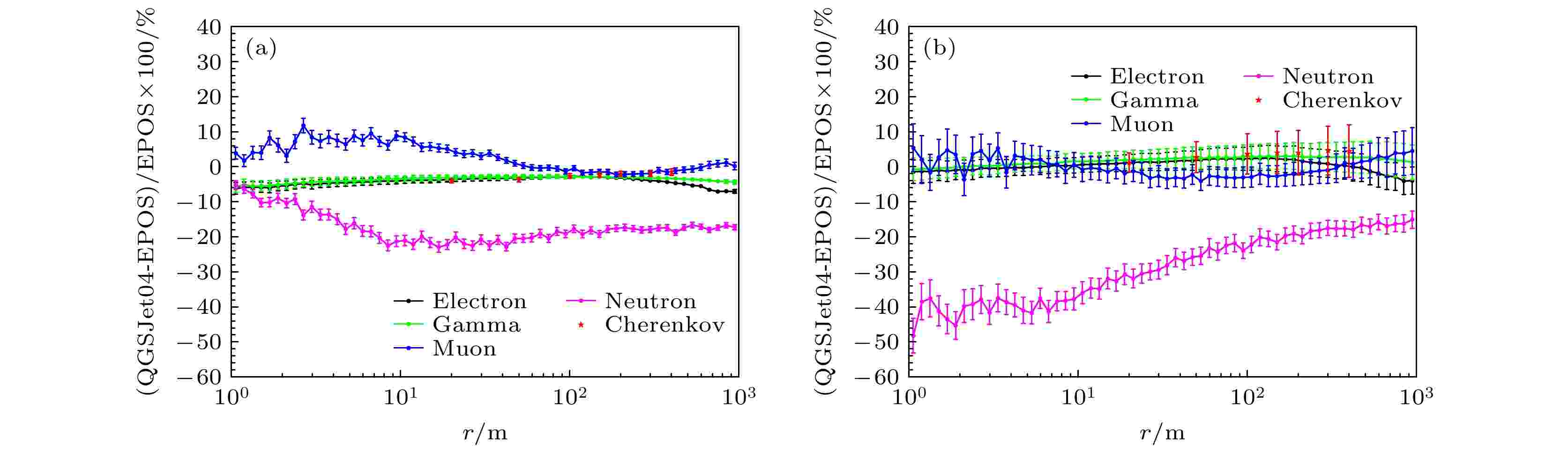
The “knee” of cosmic ray spectra reflects the maximum energy accelerated by galactic cosmic ray sources or the limit to the ability of galaxy to bind cosmic rays. The measuring of individual energy spectra is a crucial tool to ascertain the origin of the knee. However, the measuring of energy and the identifying of primary nuclei are the foundation of measuring the energy spectra of individual components. The Extensive Air Shower of cosmic rays in the knee energy region is simulated via CORSIKA software. The energy resolution for different secondary components (include electron, gamma, muon, neutron and Cherenkov light) and primary nuclei identification capability are studied. The energy reconstruction by using electromagnetic particles (electron, gamma and Cherenkov light) in the energy around “knee” is better than by using other secondary particles. The resolution is 10%–19% for proton, and 4%–8% for iron. For the case of primary nuclei identification capability, the discriminability of density of muons is best both at low (~100 TeV) and high (~10 PeV) energy, the discriminability of the shape of lateral distribution of electron and gamma-rays are good at low energy and the discriminability of density of neutrons is good at high energy. The differences between the lateral distributions of secondary particles simulated by EPOS-LHC and QGSJet-Ⅱ-04 hadronic model are studied. For electron, gamma and Cherenkov light, the differences of the number of particles are within 5%; for muon, when the perpendicular distance from the shower axis is greater than 100 m, the difference of the muon number is within 5%; for neutron, the difference in neutron number between the two models is larger than 10%. The results in this work can provide important information for selecting the secondary components and detector type during energy reconstruction and identifying the primary nuclei of cosmic rays in the knee region.
