


-
InGaAs and HgCdTe materials are widely used in short wave infrared photodetectors, which contain heavy metal elements. The massive use of the heavy metal elements naturally results in their scarcity, and the nonnegligible environmental pollution. Searching for other suitable materials for infrared devices becomes a key to solving the above problems. As a kind of abundant and eco-friendly material, Mg2Si has a high absorption coefficient in the near-infrared band. Its application in infrared detector makes it possible to replace the infrared devices containing toxic elements on the market in the future. The Mg2Si/Si avalanche photodiode(APD) with separation structure of absorption layer, charge layer and multiplication layer, with Mg2Si serving as the absorption layer, is constructed by using the Atlas module in Silvaco software. The effects of the thickness and doping concentration of the charge layer and multiplier layer on the distribution of internal electric field, punch-through voltage, breakdown voltage (Vb), C-V characteristics, and transient response of Mg2Si/Si SACM-APD are simulated. The effects of bias voltage on the I-V characteristics and spectral response are analyzed. The punch-through voltage, breakdown voltage, dark current density, gain coefficient (Mn) and the current amplification factor (M) after avalanche effect of APD are obtained after the structure optimization. According to the simulation results, the spectral response wavelength of the device is extended to 1.6 μm, so the selection of Mg2Si as the absorption layer effectively extends the spectral response band of Si based APD. When the wavelength of incident light is 1.31 µm and the optical power is 10 mW/cm2, the obtained punch-through voltage is 17.5 V, and the breakdown voltage is 50 V. When the bias voltage is 47.5 V (0.95Vb), the peak value of spectral response is 25 A/W at a wavelength of 1.1 μm, a density of dark current is about 3.6 × 10⁻⁵ A/cm2, a multiplication factor Mn is 19.6, and Mn achieves a maximum value of 102 when the device is broken down. Meanwhile, the current amplification factor M after avalanche effect is 75.4, and the current gain effect of the SACM structure is obvious. The peak value of spectral response for the pin-type photodiode in the previous study is only 0.742 A/W. Comparing with the pin-type photodiode, the spectral response of Mg2Si/Si SACM-APD is greatly improved. In this work, the structure parameters of the device are optimized, which lays a nice foundation for fabricating the high-performance devices.
-
Keywords:
- SACM-APD /
- Mg2Si/Si heterojunction /
- spectral response /
- gain coefficient
[1] 莫秋燕, 赵彦立 2011 物理学报 60 072902
 Google Scholar
Mo Q Y, Zhao Y L 2011 Acta Phys. Sin. 60 072902
Google Scholar
[2] Park S M, Grein C H 2019 J. Electron. Mater. 48 8163
Google Scholar
[3] Rogalski A 2005 Rep. Prog. Phys. 68 2267
Google Scholar
[4] Xu S J, Chua S J, Mei T, Wang X C, Zhang X H, Karunasiri G, Fan W J, Wang C H, Jiang J, Wang S, Xie X G 1998 Appl. Phys. Lett. 73 3153
Google Scholar
[5] Rogalski A 2002 Infrared. Phys. Technol. 43 187
Google Scholar
[6] Rogalski A 2011 Infrared. Phys. Technol. 54 136
Google Scholar
[7] 胡伟达, 李庆, 陈效双, 陆卫 2019 物理学报 68 120701
Google Scholar
Hu W D, Li Q, Chen X S, Lu W 2019 Acta Phys. Sin. 68 120701
Google Scholar
[8] LaBotz R 1963 J. Electrochem. Soc. 110 127
Google Scholar
[9] Kato T, Sago Y, Fujiwara H 2011 J. Appl. Phys. 110 063723
Google Scholar
[10] Borisenko V E 2000 Semiconducting Silicides (New York: Springer) pp137−179
[11] Au-Yang M Y, Cohen M L 1969 Phys. Rev. 178 1358
Google Scholar
[12] Liao Y F, Fan M H, Xie Q, Xiao Q Q, Xie J, Yu H, Wang S L, Ma X Y 2018 Appl. Surf. Sci. 403 302
Google Scholar
[13] Janega P L, McCaffrey J, Landheer D, Buchanan M, Denhoff M, Mitchel D 1988 Appl. Phys. Lett. 53 2056
Google Scholar
[14] Udono H, Tajima H, Uchikoshi M, Itakura M 2015 Jpn. J. Appl. Phys. 54 07JB06
Google Scholar
[15] Udono H, Yamanaka Y, Uchikoshi M, Isshiki M 2013 J. Phys. Chem. Solids. 74 311
Google Scholar
[16] El-Amir A A M, Ohsawa T, Nabatame T, Ohia A, Wadaa Y, Nakamuraa M, Fua K, Shimamuraa K, Ohashia N 2019 Mater. Sci. Semicond. Process. 91 222
Google Scholar
[17] 陈豪, 肖清泉, 谢泉, 王坤, 史娇娜 2019 材料导报 33 3358
Google Scholar
Chen H, Xiao Q Q, Xie Q, Wang K, Shi J N, 2019 Mater. Rep. 33 3358
Google Scholar
[18] Forrest S R, Kim O K, Smith R G 1982 Appl. Phys. Lett. 41 95
Google Scholar
[19] 张海燕, 汪琳莉, 吴琛怡, 王煜蓉, 杨雷, 潘海峰, 刘巧莉, 郭霞, 汤凯, 张忠萍, 吴光 2020 物理学报 69 074204
Google Scholar
Zhang H Y, Wang L L, Wu C Y, Wang Y R, Yang L, Pang H F, Liu Q L, Guo X, Tang K, Zhang Z P, Wu G 2020 Acta Phys. Sin. 69 074204
Google Scholar
[20] Nishida K, Taguchi K, Matsumoto Y 1979 Appl. Phys. Lett. 35 251
Google Scholar
[21] Deng Q, Wang Z, Wang S, Shao G D 2017 Sol. Energy 158 654
Google Scholar
[22] Sekino K, Midonoya M, Udono H, Yamada Y Udono H 2011 Phys. Procedia 11 171
Google Scholar
[23] Martin A G 2008 Sol. Energy Mater. Sol. Cells 92 1305
Google Scholar
[24] Park C Y, Hyun K, Kang S G, Kim H M 1995 Appl. Phys. Lett. 67 3789
Google Scholar
[25] Smetona S, Matukas J, Palenskis V, Olechnovicius M, A. Kaminskas K, Mallard R 2004 Proceedings of SPIE-Photonics North 2004: Optical Components and Devices Ottawa, Canada, September 26–29, 2004 p834
[26] 谢天, 叶新辉, 夏辉, 李菊柱, 张帅君, 姜新洋, 邓伟杰, 王文静, 李玉莹, 刘伟伟, 李翔, 李天信 2020 红外与毫米波学报 39 0583
Google Scholar
Xie T, Ye X H, Xia H, Li J Z, Zhang S J, Jiang X Y, Deng W J, Wang W J, Li Y Y, Liu W W, Li X, Li T X 2020 J. Infrared Millim. W. 39 0583
Google Scholar
[27] Yuan H, Zhang J, Kim J, Meyer C, Laquindanum J, Kimchi J, Lei J 2018 Proceedings of SPIE -Infrared Sensors, Devices, and Applications VIII San Diego, United States, August 22–23, 2018 p107660 J-1
[28] Wang Y D, Chen J, Xu J D, Li X Y 2018 Infrared Phys. Technol. 89 41
Google Scholar
[29] 施敏, 伍国珏 著 (耿莉, 张瑞智 译) 2008 半导体器件物理 (第3版) (西安: 西安交通大学出版社) 第514−523页
Sze S M, K. Ng K (translated by Geng L, Wu G J) 2008 Physics of Semiconductor Devices (3rd Ed.) (Xi’an: Xi’an Jiaotong University Press) pp514−523 (in Chinese)
[30] Lee M J, Rucker H, Choi W Y 2012 IEEE Electron Device Lett. 33 80
Google Scholar
-

图 1 SACM-APD结构示意图
Figure 1. Schematic diagram of SACM-APD.
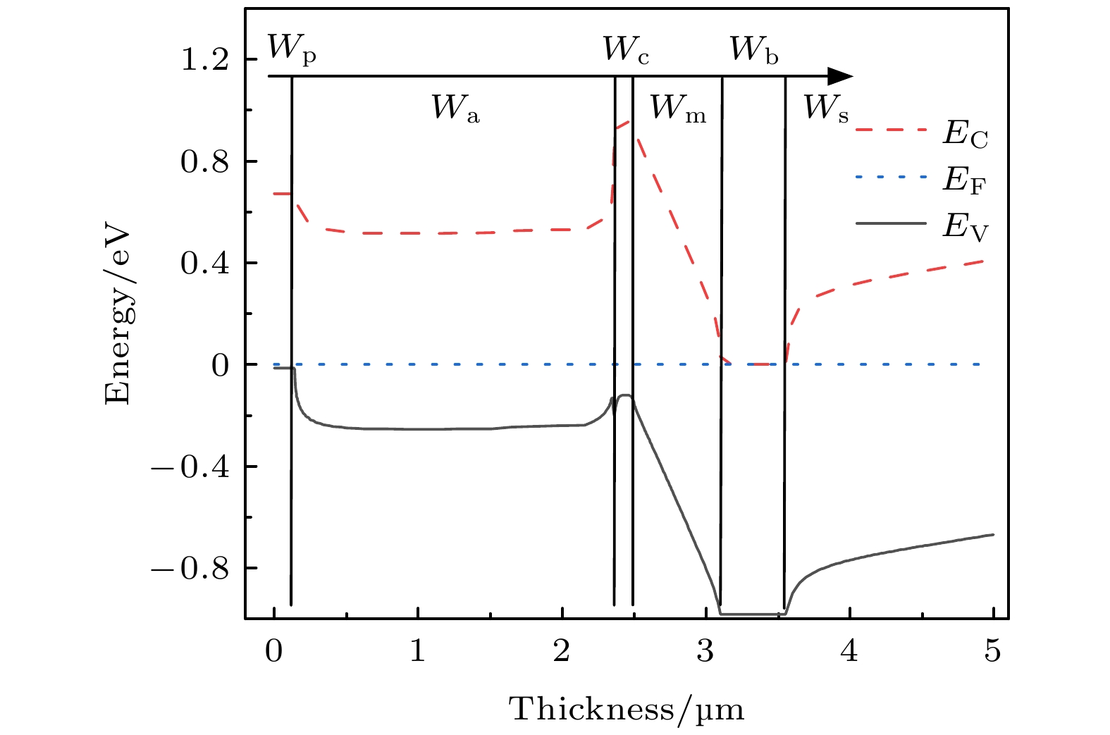
图 2 APD的能带结构图
Figure 2. Energy band structure diagram of the APD.

图 3 Mg2Si与c-Si的光学特性 (a) Mg2Si与c-Si的吸收系数(cm–1)与入射能量的关系; (b) Mg2Si与c-Si的折射率与波长的关系
Figure 3. Optical properties of Mg2Si and c-Si: (a) Absorption coefficient(cm–1) of the poly-Mg2Si and c-Si; (b) refractive Index of the poly-Mg2Si and c-Si.
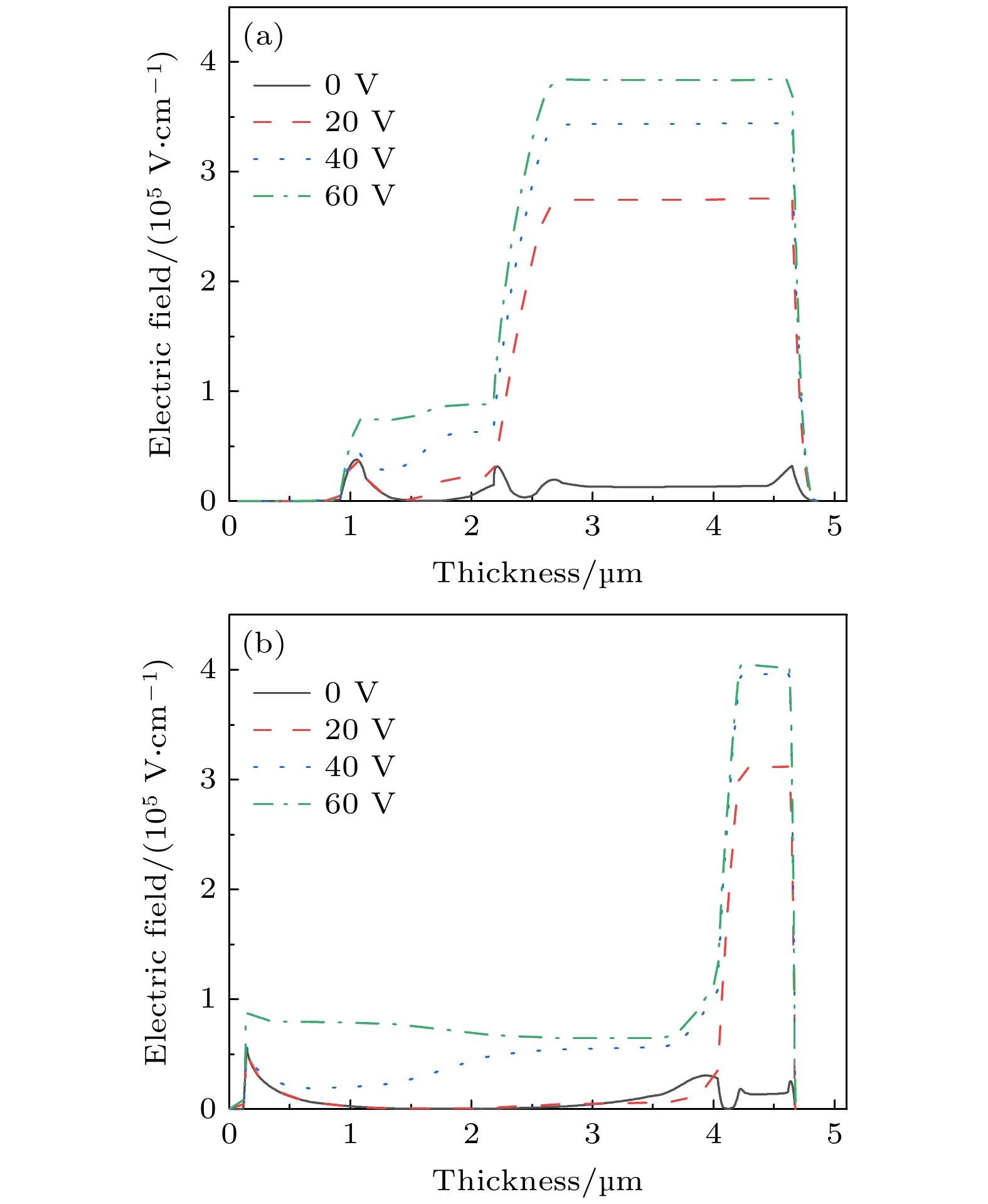
图 4 (a) 电荷层厚度为0.1 µm时器件的电场分布; (b) 电荷层厚度为0.2 µm时器件的电场分布
Figure 4. (a) Electric field distribution of the device with charge layer thickness of 0.1 µm; (b) electric field distribution of the device with charge layer thickness of 0.2 µm.
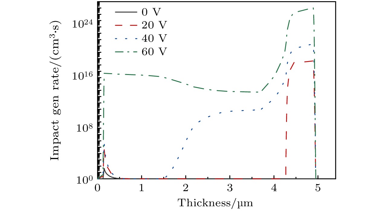
图 5 Mg2Si/Si SACM-APD器件在不同偏压下内部的载流子生成率
Figure 5. The influence of the different Bias voltage on the carrier generation rate.

图 6 倍增层不同掺杂浓度时倍增层的电场分布
Figure 6. Electric field distribution of the multiplier layer under different doping concentrations.
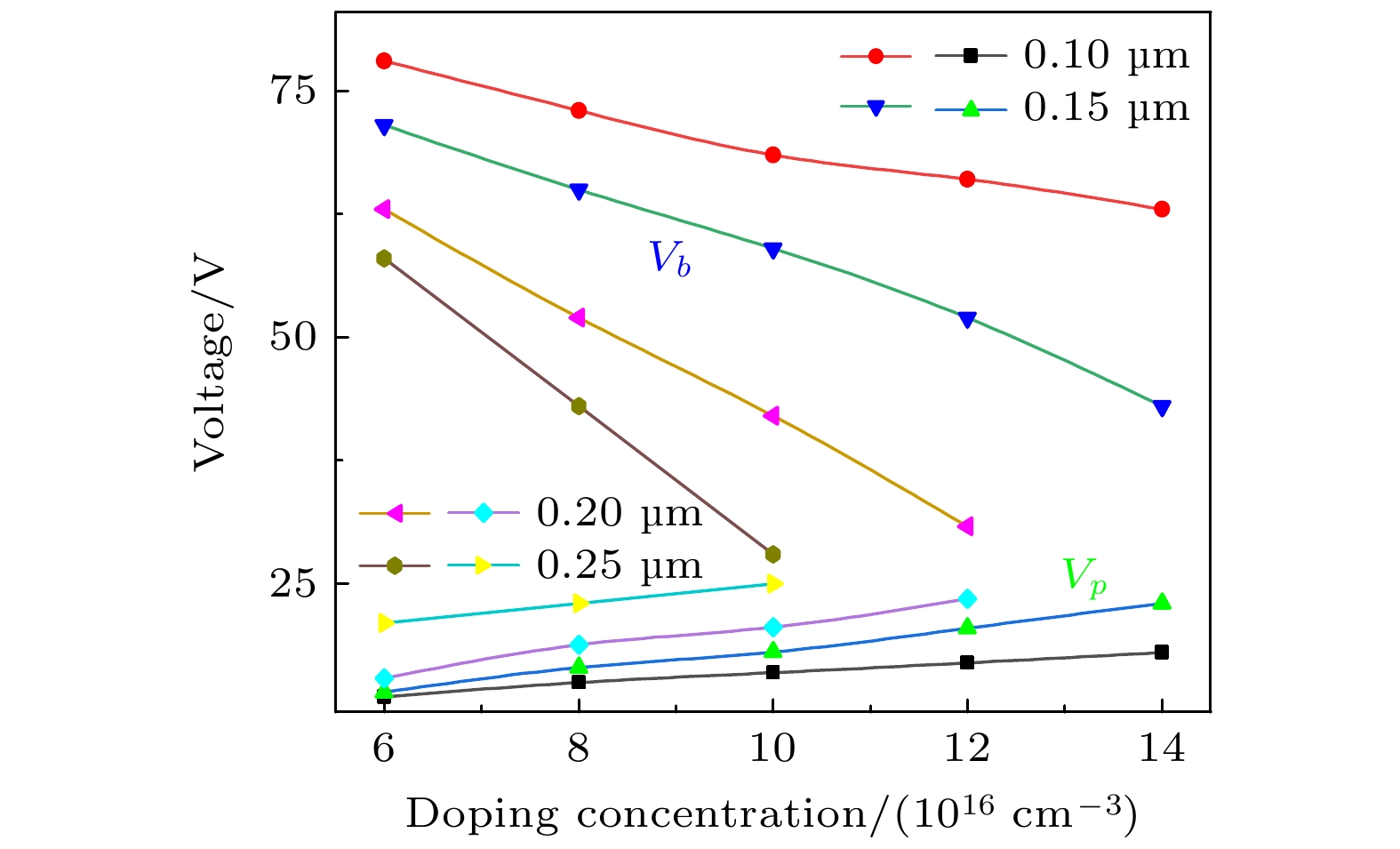
图 7 电荷层厚度、掺杂浓度与击穿电压和穿通电压之间的关系
Figure 7. The relation between the thickness and doping concentration of charge layer and the breakdown voltage, the punch-through voltage.
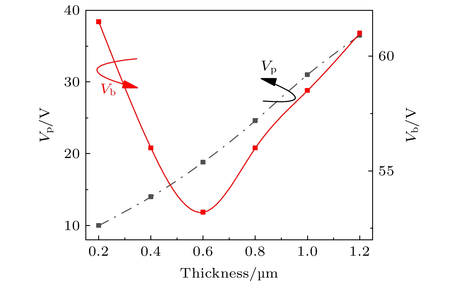
图 8 不同倍增层厚度时的击穿电压与穿通电压
Figure 8. Breakdown voltage and penetration voltage at different thicknesses of the multiplier layer.

图 9 倍增层不同掺杂浓度与穿通电压和击穿电压关系
Figure 9. Breakdown voltage and penetration voltage at different doping concentration of the multiplier layer.
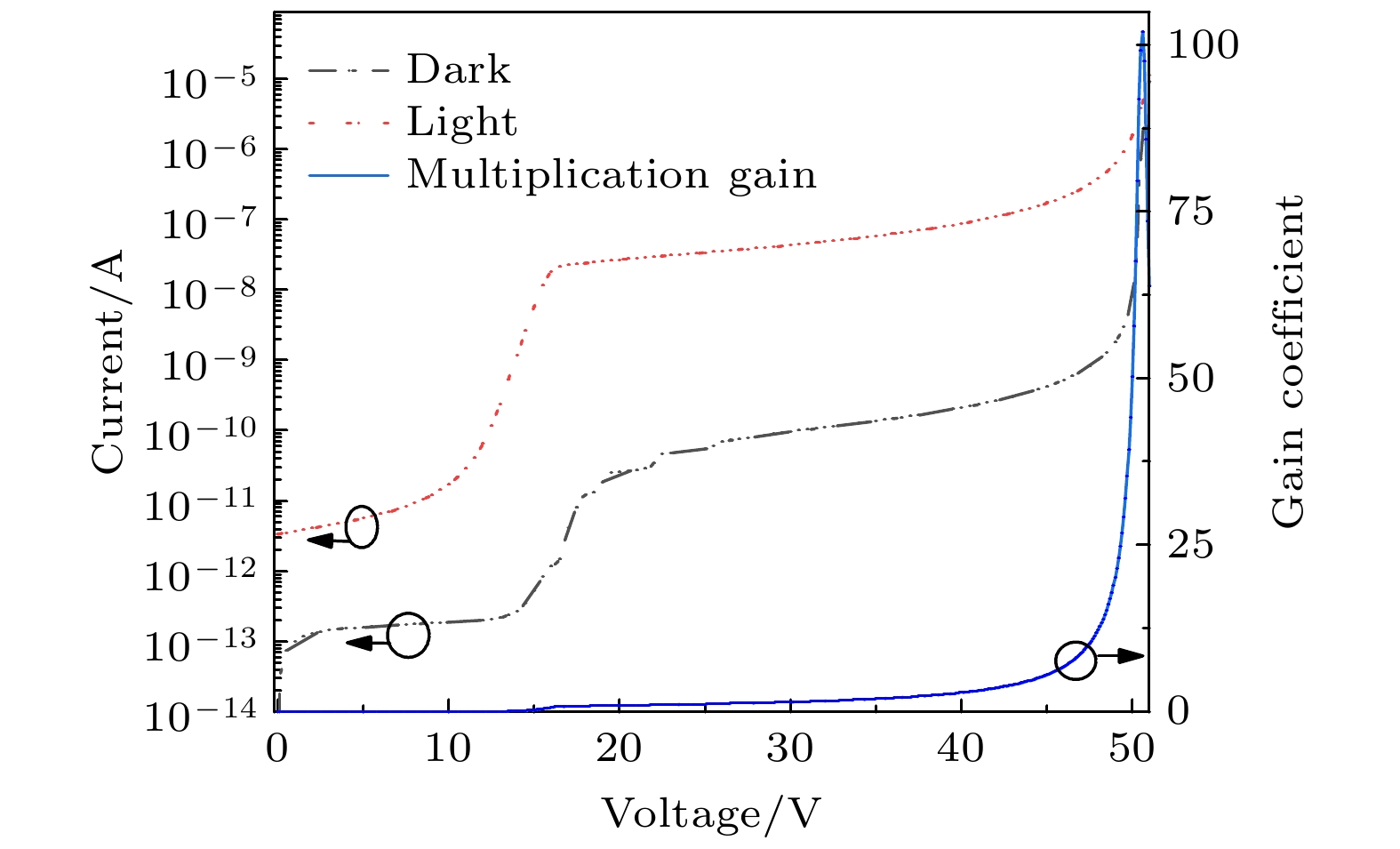
图 10 APD的I-V特性与增益系数
Figure 10. I-V characteristics and gain coefficient of APD.
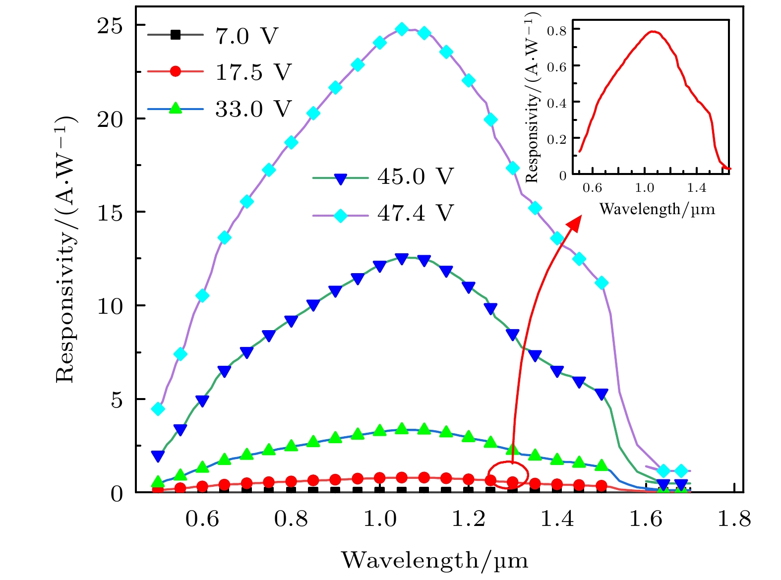
图 11 不同的偏置电压对APD光谱响应的影响
Figure 11. Effect of different bias voltages on the spectral response of APD.
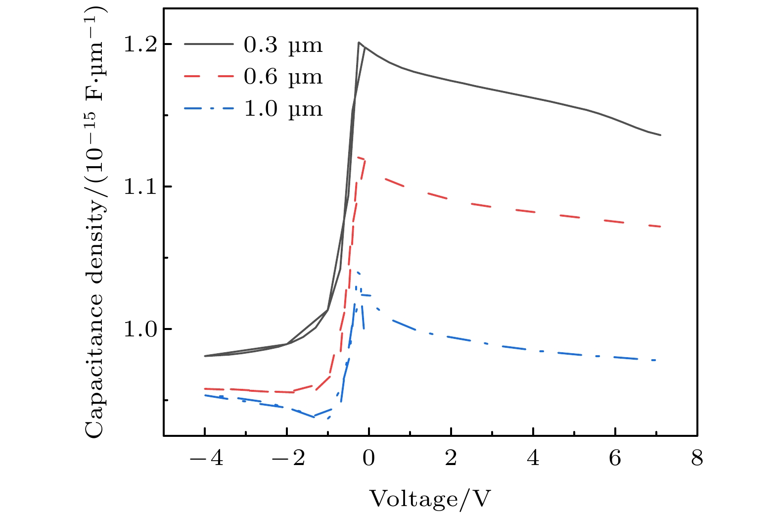
图 12 倍增层厚度对器件电容的影响
Figure 12. The influence of the thickness of multiplication layer on the capacitance of the device.
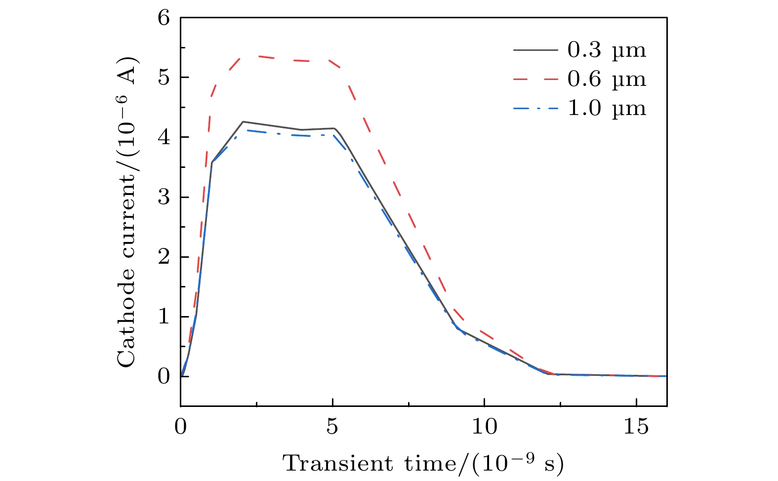
图 13 不同倍增层厚度时器件的瞬态响应
Figure 13. Transient response of the device for different thickness of the multiplication layer.
表 1 APD的结构参数
Table 1. Structural parameters of the APD.
层名 符号 厚度/μm 符号 浓度掺杂/
× 1016 cm–3金属电极层 — 0.1 — 0 Mg2Si接触层 Wp 0.15 Np 500 Mg2Si吸收层 Wa 0.6—4 Na 0.1 Si电荷层 Wc 0.1—0.3 Nc 6—14 Si倍增层 Wm 1 Nm 0.01—1 Si缓冲层 Wb 0.5 Nb 100 Si衬底 Ws 3.5 Ns 1000  DownLoad: CSV
表 3 模拟结果与目前国际水平对比
Table 3. Comparison of simulation results with current international level.
DownLoad: CSV
-
[1] 莫秋燕, 赵彦立 2011 物理学报 60 072902
Google Scholar
Mo Q Y, Zhao Y L 2011 Acta Phys. Sin. 60 072902
Google Scholar
[2] Park S M, Grein C H 2019 J. Electron. Mater. 48 8163
Google Scholar
[3] Rogalski A 2005 Rep. Prog. Phys. 68 2267
Google Scholar
[4] Xu S J, Chua S J, Mei T, Wang X C, Zhang X H, Karunasiri G, Fan W J, Wang C H, Jiang J, Wang S, Xie X G 1998 Appl. Phys. Lett. 73 3153
Google Scholar
[5] Rogalski A 2002 Infrared. Phys. Technol. 43 187
Google Scholar
[6] Rogalski A 2011 Infrared. Phys. Technol. 54 136
Google Scholar
[7] 胡伟达, 李庆, 陈效双, 陆卫 2019 物理学报 68 120701
Google Scholar
Hu W D, Li Q, Chen X S, Lu W 2019 Acta Phys. Sin. 68 120701
Google Scholar
[8] LaBotz R 1963 J. Electrochem. Soc. 110 127
Google Scholar
[9] Kato T, Sago Y, Fujiwara H 2011 J. Appl. Phys. 110 063723
Google Scholar
[10] Borisenko V E 2000 Semiconducting Silicides (New York: Springer) pp137−179
[11] Au-Yang M Y, Cohen M L 1969 Phys. Rev. 178 1358
Google Scholar
[12] Liao Y F, Fan M H, Xie Q, Xiao Q Q, Xie J, Yu H, Wang S L, Ma X Y 2018 Appl. Surf. Sci. 403 302
Google Scholar
[13] Janega P L, McCaffrey J, Landheer D, Buchanan M, Denhoff M, Mitchel D 1988 Appl. Phys. Lett. 53 2056
Google Scholar
[14] Udono H, Tajima H, Uchikoshi M, Itakura M 2015 Jpn. J. Appl. Phys. 54 07JB06
Google Scholar
[15] Udono H, Yamanaka Y, Uchikoshi M, Isshiki M 2013 J. Phys. Chem. Solids. 74 311
Google Scholar
[16] El-Amir A A M, Ohsawa T, Nabatame T, Ohia A, Wadaa Y, Nakamuraa M, Fua K, Shimamuraa K, Ohashia N 2019 Mater. Sci. Semicond. Process. 91 222
Google Scholar
[17] 陈豪, 肖清泉, 谢泉, 王坤, 史娇娜 2019 材料导报 33 3358
Google Scholar
Chen H, Xiao Q Q, Xie Q, Wang K, Shi J N, 2019 Mater. Rep. 33 3358
Google Scholar
[18] Forrest S R, Kim O K, Smith R G 1982 Appl. Phys. Lett. 41 95
Google Scholar
[19] 张海燕, 汪琳莉, 吴琛怡, 王煜蓉, 杨雷, 潘海峰, 刘巧莉, 郭霞, 汤凯, 张忠萍, 吴光 2020 物理学报 69 074204
Google Scholar
Zhang H Y, Wang L L, Wu C Y, Wang Y R, Yang L, Pang H F, Liu Q L, Guo X, Tang K, Zhang Z P, Wu G 2020 Acta Phys. Sin. 69 074204
Google Scholar
[20] Nishida K, Taguchi K, Matsumoto Y 1979 Appl. Phys. Lett. 35 251
Google Scholar
[21] Deng Q, Wang Z, Wang S, Shao G D 2017 Sol. Energy 158 654
Google Scholar
[22] Sekino K, Midonoya M, Udono H, Yamada Y Udono H 2011 Phys. Procedia 11 171
Google Scholar
[23] Martin A G 2008 Sol. Energy Mater. Sol. Cells 92 1305
Google Scholar
[24] Park C Y, Hyun K, Kang S G, Kim H M 1995 Appl. Phys. Lett. 67 3789
Google Scholar
[25] Smetona S, Matukas J, Palenskis V, Olechnovicius M, A. Kaminskas K, Mallard R 2004 Proceedings of SPIE-Photonics North 2004: Optical Components and Devices Ottawa, Canada, September 26–29, 2004 p834
[26] 谢天, 叶新辉, 夏辉, 李菊柱, 张帅君, 姜新洋, 邓伟杰, 王文静, 李玉莹, 刘伟伟, 李翔, 李天信 2020 红外与毫米波学报 39 0583
Google Scholar
Xie T, Ye X H, Xia H, Li J Z, Zhang S J, Jiang X Y, Deng W J, Wang W J, Li Y Y, Liu W W, Li X, Li T X 2020 J. Infrared Millim. W. 39 0583
Google Scholar
[27] Yuan H, Zhang J, Kim J, Meyer C, Laquindanum J, Kimchi J, Lei J 2018 Proceedings of SPIE -Infrared Sensors, Devices, and Applications VIII San Diego, United States, August 22–23, 2018 p107660 J-1
[28] Wang Y D, Chen J, Xu J D, Li X Y 2018 Infrared Phys. Technol. 89 41
Google Scholar
[29] 施敏, 伍国珏 著 (耿莉, 张瑞智 译) 2008 半导体器件物理 (第3版) (西安: 西安交通大学出版社) 第514−523页
Sze S M, K. Ng K (translated by Geng L, Wu G J) 2008 Physics of Semiconductor Devices (3rd Ed.) (Xi’an: Xi’an Jiaotong University Press) pp514−523 (in Chinese)
[30] Lee M J, Rucker H, Choi W Y 2012 IEEE Electron Device Lett. 33 80
Google Scholar

 DownLoad:
Catalog
Metrics
- Abstract views: 5911
- PDF Downloads: 139
- Cited By: 0
