


-
The Cu2ZnSnS4 (CZTS) solar cell prepared on Si substrate has an advantage of low lattice mismatch between CZTS and Si substrate, but the conversion efficiency of reported p-CZTS/n-Si solar cells is still low at present. In this work, the CZTS solar cells on Si substrate are calculated numerically by heterojunction solar cell simulation software Afors-het. The calculated results show that the p-CZTS and n-Si act as window layer and absorber respectively in the p-CZTS/n-Si solar cell because the band gap of p-CZTS is larger than that of n-Si. The conversion efficiency of p-CZTS/n-Si solar cell increases as the thickness of p-CZTS window layer decreases. The highest calculated conversion efficiency of p-CZTS/n-Si solar cell is 18.57%. In the best p-CZTS/n-Si solar cell, most of the incident light cannot pass through the p-CZTS window layer due to the high absorption coefficient of p-CZTS, which limits the conversion efficiency of solar cell. In order to solve the problems existing in the p-CZTS/n-Si structure, a novel n-ZnO:Al/i-ZnO/n-CdS/p-CZTS/p-Si solar cell structure is proposed, where n-ZnO:Al and i-ZnO are window layers, n-CdS is buffer layer, p-CZTS is absorber, and p-Si is substrate and back electrode. The dark current density-voltage (J-V) characteristic curves of p-CZTS/p-Si structure varying with the thickness and doping concentration of p-Si and the doping concentration of p-CZTS are calculated to investigate the feasibility of p-Si as a back electrode of p-CZTS. All the calculated J-V characteristic curves of p-CZTS/p-Si structure are linear, indicating the formation of ohmic contact between p-CZTS and p-Si. The photovoltaic properties of n-ZnO:Al/i-ZnO/n-CdS/p-CZTS/p-Si solar cell are further calculated. The built-in electric field distributed in n-ZnO:Al, i-ZnO, n-CdS, and p-CZTS contribute to the collection of photo-generated carriers. The conversion efficiency of n-ZnO:Al/i-ZnO/n-CdS/p-CZTS/p-Si solar cell is enhanced with the decrease of the thickness of p-Si and the increase of doping concentrations of p-Si and p-CZTS and the thickness of p-CZTS. Without considering the effect of parasitic series resistance and parallel resistance and defect states, the highest conversion efficiency of ideal n-ZnO:Al/i-ZnO/n-CdS/p-CZTS/p-Si solar cell is 28.41%. The calculated results in this work show that the n-ZnO:Al/i-ZnO/n-CdS/p-CZTS/p-Si solar cell has an appropriate structure for CZTS solar cell on Si substrate.
-
Keywords:
- Cu2ZnSnS4 /
- Si /
- back electrode /
- photovoltaic property
[1] Matsushita H, Ichikawa T, Katsui A 2005 J. Mater. Sci. 40 2003
 Google Scholar
[2] Steinhagen C, Panthani M G, Akhavan V, Goodfellow B, Koo B, Korgel B A 2009 J. Am. Chem. Soc. 131 12554
Google Scholar
[3] Todorov T, Gunawan O, Chey S J, De Monsabert T G, Prabhakar A, Mitzi D B 2011 Thin Solid Films 519 7378
Google Scholar
[4] Scragg J J, Dale P J, Peter L M, Zoppi G, Forbes I 2008 Phys. Status Solidi B 245 1772
Google Scholar
[5] Maklavani S E, Mohammadnejad S 2020 Sol. Energy 204 489
Google Scholar
[6] Nadaraja M, Singh O P, Gour K S, Singh V N 2020 J. Nanosci. Nanotechnol. 20 3925
Google Scholar
[7] Akcay N, Ataser T, Ozen Y, Ozcelik S 2020 Thin Solid Films 704 138028
Google Scholar
[8] Karade V, Lokhande A, Babar P, Gang M G, Suryawanshi M, Patil P, Kim J H 2019 Sol. Energy Mater. Sol. Cells 200 109911
Google Scholar
[9] Ataca C, Topsakal M, Akturk E, Ciraci S 2011 J. Phys. Chem. C 115 16354
Google Scholar
[10] Song N, Young M, Liu F Y, Erslev P, Wilson S, Harvey S P, Teeter G, Huang Y D, Hao X J, Green M A 2015 Appl. Phys. Lett. 106 252102
Google Scholar
[11] Xu J X, Yang Y Z, Cao Z M, Xie Z W 2016 Optik 127 1567
Google Scholar
[12] Shin B H, Zhu Y, Gershon T, Bojarczuk N A, Guha S 2014 Thin Solid Films 556 9
Google Scholar
[13] Sheng X, Wang L, Tian Y, Luo Y P, Chang L T, Yang D R 2013 J. Mater. Sci.-Mater. Electron. 24 548
Google Scholar
[14] 李琳, 文亚南, 董燕, 汪壮兵, 梁齐 2012 真空 49 45
Google Scholar
Li L, Wen Y N, Dong Y, Wang Z B, Liang Q 2012 Vacuum 49 45
Google Scholar
[15] Yeh M Y, Lei P H, Lin S H, Yang C D 2016 Materials 9 526
Google Scholar
[16] Singh S, Katiyar A K, Midya A, Ghorai A, Ray S K 2017 Nanotechnology 28 435704
Google Scholar
[17] Wang W, Winkler M T, Gunawan O, Gokmen T, Todorov T K, Zhu Y, Mitzi D B 2014 Adv. Energy Mater. 4 1301465
Google Scholar
[18] Varache R, Leendertz C, Gueunier-farret M E, Haschke J, Munoz D, Korte L 2015 Sol. Energy Mater. Sol. Cells 141 14
Google Scholar
[19] Amin N, Hossain M I, Chelvanathan P, Uzzaman A M, Sopian K 2010 International Conference on Electrical & Computer Engineering Dhaka, Bangladesh, December 18–20, 2010 p730
[20] Jiang F, Shen H L, Wang W, Zhang L 2011 Appl. Phys. Express 4 074101
Google Scholar
[21] 许佳雄, 姚若河 2012 物理学报 61 187304
Google Scholar
Xu J X, Yao R H 2012 Acta Phys. Sin. 61 187304
Google Scholar
[22] Prabeesh P, Selvam I P, Potty S N 2016 Thin Solid Films 606 94
Google Scholar
[23] Ali K, Khan S A, Jafri M Z M 2014 Sol. Energy 101 1
Google Scholar
[24] Yoshikawa K, Kawasaki H, Yoshida W, Irie T, Konishi K, Nakano K, Uto T, Adachi D, Kanematsu M, Uzu H, Yamamoto K 2017 Nat. Energy 2 17032
Google Scholar
-
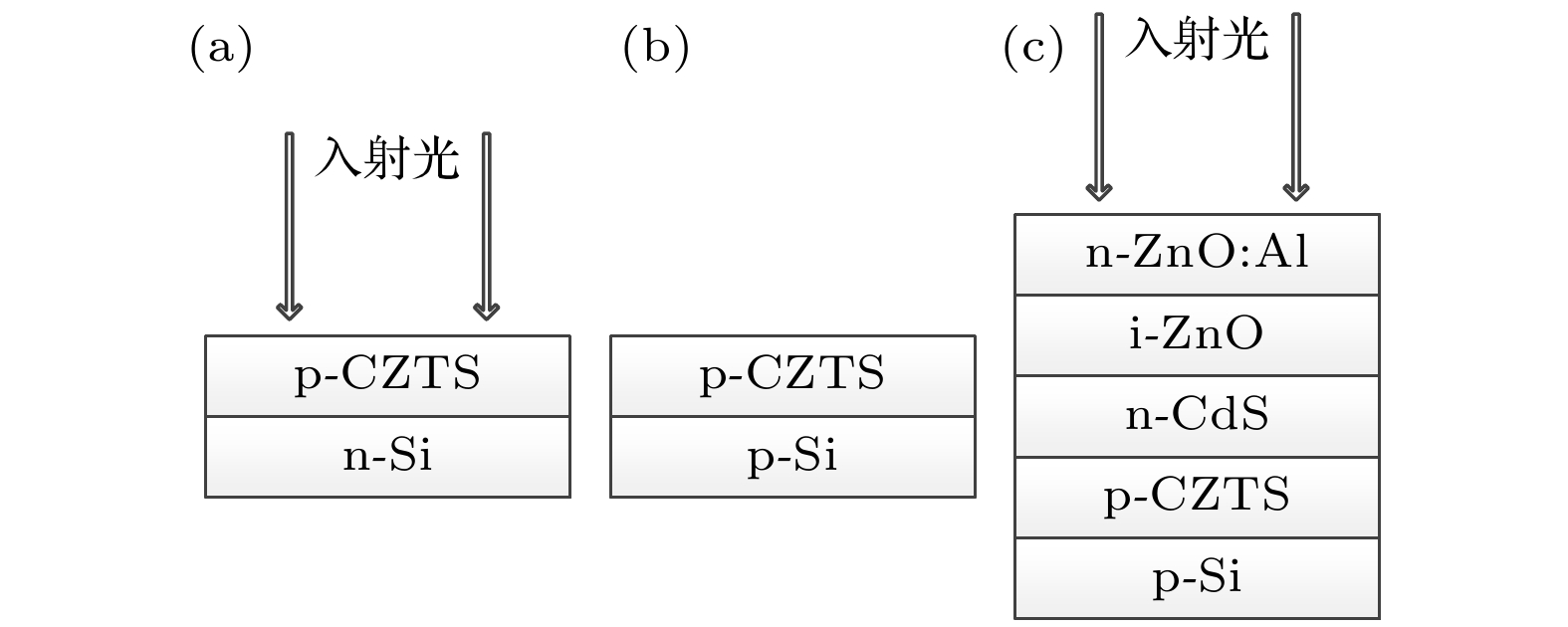
图 1 仿真结构示意图 (a) p-CZTS/n-Si; (b) p-CZTS/p-Si; (c) n-ZnO:Al/i-ZnO/n-CdS/p-CZTS/p-Si
Figure 1. Diagrams of different structures: (a) p-CZTS/n-Si; (b) p-CZTS/p-Si; (c) n-ZnO:Al/i-ZnO/CdS/CZTS/p-Si.

图 2 p-CZTS/n-Si太阳能电池性能随 (a) n-Si的厚度dn-Si, (b) n-Si的掺杂浓度Nn-Si, (c) p-CZTS的厚度dp-CZTS, (d) p-CZTS的掺杂浓度Np-CZTS的变化关系
Figure 2. The performances of p-CZTS/n-Si solar cell with the changes of (a) the thickness of n-Si (dn-Si), (b) the doping concentration of n-Si (Nn-Si), (c) the thickness of p-CZTS (dp-CZTS), (d) the doping concentration of p-CZTS (Np-CZTS).
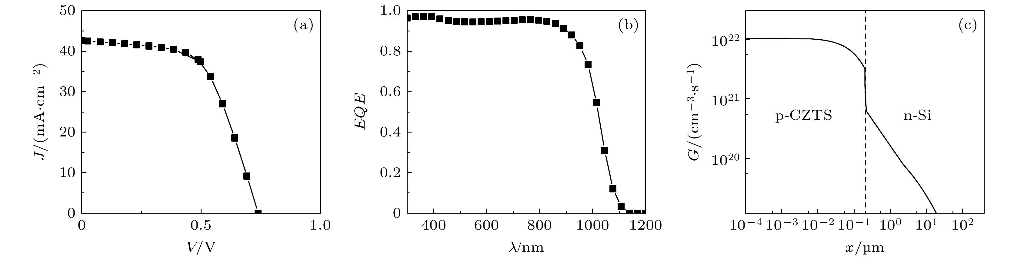
图 3 最优p-CZTS/n-Si太阳能电池的 (a) J–V特性曲线, (b)光谱响应, (c)载流子产生率分布图
Figure 3. The (a) J–V characteristic curve, (b) spectral response, (c) generation rate distribution of the optimal p-CZTS/n-Si solar cell

图 4 p-CZTS/p-Si的J-V特性曲线随p-Si厚度dp-Si的变化
Figure 4. J-V characteristic curves of p-CZTS/p-Si with the change of the thickness of p-Si (dp-Si).

图 5 p-CZTS/p-Si的J-V特性曲线随p-Si掺杂浓度Np-Si的变化
Figure 5. J-V characteristic curves of p-CZTS/p-Si with the change of the doping concentration of p-Si (Np-Si).

图 6 p-Si掺杂浓度为 (a) 1 × 1015 cm–3, (b) 1 × 1017 cm–3, (c) 1 × 1019 cm–3时, p-CZTS/p-Si的能带图
Figure 6. Band diagrams of p-CZTS/p-Si when the doping concentrations of p-Si are (a) 1 × 1015 cm–3, (b) 1 × 1017 cm–3, (c) 1 × 1019 cm–3

图 7 p-CZTS/p-Si的J-V特性曲线随p-CZTS掺杂浓度Np-CZTS的变化
Figure 7. J-V characteristic curves of p-CZTS/p-Si with the change of the doping concentration of p-CZTS (Np-CZTS).

图 8 p-CZTS掺杂浓度为 (a) 1 × 1015 cm–3, (b) 1 × 1017 cm–3, (c) 1 × 1019 cm–3时, p-CZTS/p-Si的能带图
Figure 8. Band diagrams of p-CZTS/p-Si when the doping concentrations of p-CZTS are (a) 1 × 1015 cm–3, (b) 1 × 1017 cm–3, (c) 1 × 1019 cm–3.
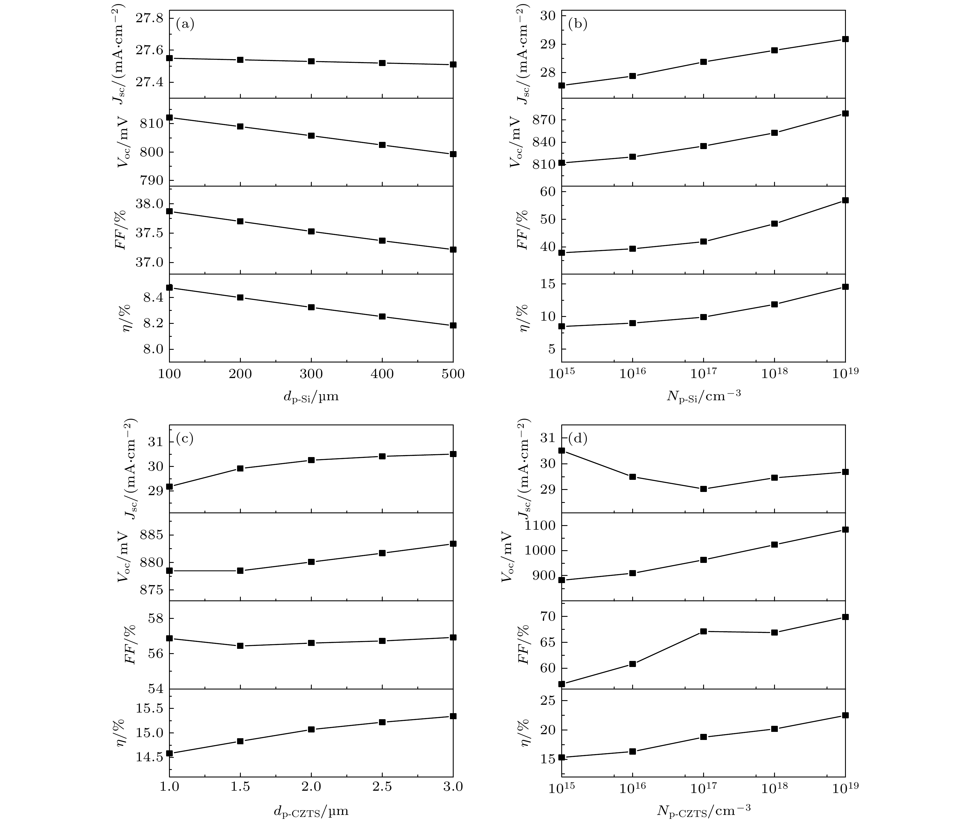
图 9 n-ZnO:Al/i-ZnO/n-CdS/p-CZTS/p-Si太阳能电池的性能随 (a) p-Si厚度dp-Si, (b) p-Si掺杂浓度Np-Si, (c) p-CZTS厚度dp-CZTS, (d) p-CZTS掺杂浓度Np-CZTS的变化关系
Figure 9. The performances of n-ZnO:Al/i-ZnO/n-CdS/p-CZTS/p-Si solar cell with the changes of (a) the thickness of p-Si (dp-Si), (b) the doping concentration of p-Si (Np-Si), (c) the thickness of p-CZTS (dp-CZTS), (d) the doping concentration of p-CZTS (Np-CZTS).

图 10 优化的n-ZnO:Al/i-ZnO/n-CdS/p-CZTS/p-Si太阳能电池的 (a) J–V特性曲线, (b)光谱响应, (c)内建电场, (d)能带图
Figure 10. The (a) J–V characteristic curve, (b) spectral response, (c) built-in electric field, (d) band diagram of the optimal n-ZnO:Al/i-ZnO/n-CdS/p-CZTS/p-Si solar cell.
表 1 仿真参数取值
Table 1. Simulated parameters.
参数 p-CZTS n-CdS i-ZnO n-ZnO p-Si n-Si 介电常数 10 10 9 9 11.9 11.9 电子亲和能/eV 3.8 4.2 4.6 4.6 4.05 4.05 禁带宽度/eV 1.53 2.4 3.3 3.3 1.12 1.12 导带有效密度/cm–3 2.2 × 10¹⁸ 1.8 × 10¹⁹ 2.2 × 10¹⁸ 2.2 × 10¹⁸ 3.32 × 10¹⁸ 3.32 × 10¹⁸ 价带有效密度/cm–3 1.8 × 10¹⁹ 2.4 × 10¹⁸ 1.8 × 10¹⁹ 1.8 × 10¹⁹ 1.44 × 10¹⁹ 1.44 × 10¹⁹ 电子迁移率/(cm2·V–1·s–1) 100 100 100 100 1450 1450 空穴迁移率/(cm2·V–1·s–1) 57.6 25 25 25 500 500 受主掺杂浓度/cm–3 变量 0 0 0 变量 0 施主掺杂浓度/cm–3 0 1 × 10¹⁷ 1 × 10⁵ 1 × 10¹⁸ 0 变量 缺陷浓度/cm–3 1 × 10¹² 6 × 10¹⁶ 1 × 10¹⁷ 1 × 10¹⁷ — — 电子俘获截面/cm2 4.13 × 10⁻¹⁴ 1 × 10–17 1 × 10–12 1 × 10–12 — — 空穴俘获截面/cm2 4.13 × 10⁻¹¹ 1 × 10–13 1 × 10–15 1 × 10–15 — — 厚度/μm 变量 0.05 0.2 0.2 变量 变量  DownLoad: CSV
-
[1] Matsushita H, Ichikawa T, Katsui A 2005 J. Mater. Sci. 40 2003
Google Scholar
[2] Steinhagen C, Panthani M G, Akhavan V, Goodfellow B, Koo B, Korgel B A 2009 J. Am. Chem. Soc. 131 12554
Google Scholar
[3] Todorov T, Gunawan O, Chey S J, De Monsabert T G, Prabhakar A, Mitzi D B 2011 Thin Solid Films 519 7378
Google Scholar
[4] Scragg J J, Dale P J, Peter L M, Zoppi G, Forbes I 2008 Phys. Status Solidi B 245 1772
Google Scholar
[5] Maklavani S E, Mohammadnejad S 2020 Sol. Energy 204 489
Google Scholar
[6] Nadaraja M, Singh O P, Gour K S, Singh V N 2020 J. Nanosci. Nanotechnol. 20 3925
Google Scholar
[7] Akcay N, Ataser T, Ozen Y, Ozcelik S 2020 Thin Solid Films 704 138028
Google Scholar
[8] Karade V, Lokhande A, Babar P, Gang M G, Suryawanshi M, Patil P, Kim J H 2019 Sol. Energy Mater. Sol. Cells 200 109911
Google Scholar
[9] Ataca C, Topsakal M, Akturk E, Ciraci S 2011 J. Phys. Chem. C 115 16354
Google Scholar
[10] Song N, Young M, Liu F Y, Erslev P, Wilson S, Harvey S P, Teeter G, Huang Y D, Hao X J, Green M A 2015 Appl. Phys. Lett. 106 252102
Google Scholar
[11] Xu J X, Yang Y Z, Cao Z M, Xie Z W 2016 Optik 127 1567
Google Scholar
[12] Shin B H, Zhu Y, Gershon T, Bojarczuk N A, Guha S 2014 Thin Solid Films 556 9
Google Scholar
[13] Sheng X, Wang L, Tian Y, Luo Y P, Chang L T, Yang D R 2013 J. Mater. Sci.-Mater. Electron. 24 548
Google Scholar
[14] 李琳, 文亚南, 董燕, 汪壮兵, 梁齐 2012 真空 49 45
Google Scholar
Li L, Wen Y N, Dong Y, Wang Z B, Liang Q 2012 Vacuum 49 45
Google Scholar
[15] Yeh M Y, Lei P H, Lin S H, Yang C D 2016 Materials 9 526
Google Scholar
[16] Singh S, Katiyar A K, Midya A, Ghorai A, Ray S K 2017 Nanotechnology 28 435704
Google Scholar
[17] Wang W, Winkler M T, Gunawan O, Gokmen T, Todorov T K, Zhu Y, Mitzi D B 2014 Adv. Energy Mater. 4 1301465
Google Scholar
[18] Varache R, Leendertz C, Gueunier-farret M E, Haschke J, Munoz D, Korte L 2015 Sol. Energy Mater. Sol. Cells 141 14
Google Scholar
[19] Amin N, Hossain M I, Chelvanathan P, Uzzaman A M, Sopian K 2010 International Conference on Electrical & Computer Engineering Dhaka, Bangladesh, December 18–20, 2010 p730
[20] Jiang F, Shen H L, Wang W, Zhang L 2011 Appl. Phys. Express 4 074101
Google Scholar
[21] 许佳雄, 姚若河 2012 物理学报 61 187304
Google Scholar
Xu J X, Yao R H 2012 Acta Phys. Sin. 61 187304
Google Scholar
[22] Prabeesh P, Selvam I P, Potty S N 2016 Thin Solid Films 606 94
Google Scholar
[23] Ali K, Khan S A, Jafri M Z M 2014 Sol. Energy 101 1
Google Scholar
[24] Yoshikawa K, Kawasaki H, Yoshida W, Irie T, Konishi K, Nakano K, Uto T, Adachi D, Kanematsu M, Uzu H, Yamamoto K 2017 Nat. Energy 2 17032
Google Scholar

 DownLoad:
Catalog
Metrics
- Abstract views: 4135
- PDF Downloads: 59
- Cited By: 0
