


-
Silicon-based optoelectronics, using the mature silicon-based microelectronic complementary metal oxide semiconductor (CMOS) manufacturing process, is a large-scale optoelectronic integration platform that has attracted much attention. Surface plasmonic devices have also received extensive attention in the past decades, and especially the silicon-based surface plasmonic nanofocusing devices have become a research hotspot. Typical nanofocusing structures include chirped surface gratings, plasmonic Fresnel zone plate, nano-slit array, tapered metal tips. However, there occur some inevitable problems in these devices, such as the fine structure being too complex to be fabricated and too large transmission loss of metal slot waveguide. In this work, an ultra-compact hybrid surface plasmon nanofocusing device is designed and fabricated by the silicon-based optoelectronic technology, and the nanofocusing performance of the device is also experimentally verified. The hybrid surface plasmon nanofocusing devices are fabricated on a silicon-on-insulator (SOI) wafer by electron beam lithography (EBL) system. The silicon wire waveguides, tapers and the thin silicon strips in the middle of nanofocusing regions are patterned in only one step EBL. The gold layer is formed by a deposition and lift-off process, and then a partially etching process is introduced to make the thickness of the middle thin silicon strips the same as that of the gold layer. With a 1.23-μm-long tapered structure, our nanofocusing devices focus the light field of a silicon strip waveguide into a hybrid surface plasmon waveguide, making non-resonant optical field increase 20 times in the 1550 nm near-infrared band experimentally. The entire insertion loss is about 4.6 dB, and the mode area of the nanofocusing area is about
${\left( {\lambda /n} \right)^2}/640$ which is over 300 times smaller than that of the input silicon waveguide. When the middle slot silicon waveguide width WSi = 120 nm, the insertion loss reaches a minimum value of 2.8 dB. In our design, we adopt the design of silicon-based hybrid plasmonic waveguides. In this design, a layer of material with low refractive index is inserted between the metal layer and the silicon layer to act as a “container” of light field, which makes this silicon-based hybrid plasmonic waveguides have less loss than the traditional metal plasmonic waveguides, and can still maintain high optical field localization. Such silicon-based hybrid surface plasmon nanofocusing devices with simple structures and excellent performances are promising alternatives for future applications in optical field manipulation, optical sensing, nonlinear optical devices, and optical phase-change storage.-
Keywords:
- silicon-based optoelectronics /
- silicon hybrid plasmonics /
- on-chip nanofocusing /
- large-scale optoelectronic integration
[1] Zhou Z, Yin B, Deng Q, Li X, Cui J 2015 Photonics Res. 3 B28
 Google Scholar
[2] Zhou Z, Yin B, Michel J 2015 Light Sci. Appl. 4 e358
Google Scholar
[3] Dai D, Bowers J E 2014 Nanophotonics 3 283
Google Scholar
[4] Dai D, Bauters J, Bowers J E 2012 Light Sci. Appl. 1 e1
Google Scholar
[5] Zhou Z, Bai B, Liu L 2019 IEEE J. Sel. Topics Quantum Electron 25 4600413
Google Scholar
[6] Bai B, Yang F, Zhou Z 2019 Photonics Res. 7 289
Google Scholar
[7] Chen R, Bai B, Yang F, Zhou Z 2020 Optics Lett. 45 803
Google Scholar
[8] Chen R, Bai B, Zhou Z 2020 Photonics Res. 8 1197
Google Scholar
[9] Zhu K, Xu P, Sun P, Liu X, Li H, Zhou Z 2020 An Ultra-compact Broadband TE-pass Nanofocusing Structure (Beijing: Optical Society of America)
[10] Zhu K, Xu P, Sun P, Liu X, Li H, Zhou Z 2020 Low Loss, High Extinction Ratio Plasmonic Spot Size Converter (Beijing: Optical Society of America)
[11] Sun P F, Xu P F, Zhu K J, Zhou Z P 2021 Photonics 8 482
Google Scholar
[12] Gramotnev D K, Bozhevolnyi S I 2014 Nat. Photonics 8 13
Google Scholar
[13] Diaz F J, Li G, de Sterke C M, Kuhlmey B T, Palomba S 2016 J. Opt. Soc. Am. B 33 957
Google Scholar
[14] Diaz F J, Hatakeyama T, Rho J, Wang Y, O Brien K, Zhang X, Martijn De Sterke C, Kuhlmey B T, Palomba S 2016 Optics Express 24 545
Google Scholar
[15] Kim S, Lim Y, Kim H, Park J, Lee B 2008 Appl. Phys. Lett. 92 13103
Google Scholar
[16] Fu Y, Zhou W, Lim L E N, Du C L, Luo X G 2007 Appl. Phys. Lett. 91 61124
Google Scholar
[17] Mote R G, Yu S F, Ng B K, Zhou W, Lau S P 2008 Optics Express 16 9554
Google Scholar
[18] Shi H, Wang C, Du C, Luo X, Dong X, Gao H 2005 Optics Express 13 6815
Google Scholar
[19] Min C, Wang P, Jiao X, Deng Y, Ming H 2008 Appl. Phys. B 90 97
Google Scholar
[20] Stockman M I 2004 Phys. Rev. Lett. 93 137404
Google Scholar
[21] Babadjanyan A J, Margaryan N L, Nerkararyan K V 2000 J. Appl. Phys. 87 3785
Google Scholar
[22] Issa N A, Guckenberger R 2007 Plasmonics 2 31
Google Scholar
[23] Gramotnev D K, Vogel M W, Stockman M I 2008 J. Appl. Phys. 104 34311
Google Scholar
[24] Veronis G, Fan S 2007 Optics Express 15 1211
Google Scholar
[25] Chen L, Shakya J, Lipson M 2006 Optics Letters 31 2133
Google Scholar
[26] Ono M, Taniyama H, Xu H, Tsunekawa M, Kuramochi E, Nozaki K, Notomi M 2016 Optica 3 999
Google Scholar
-
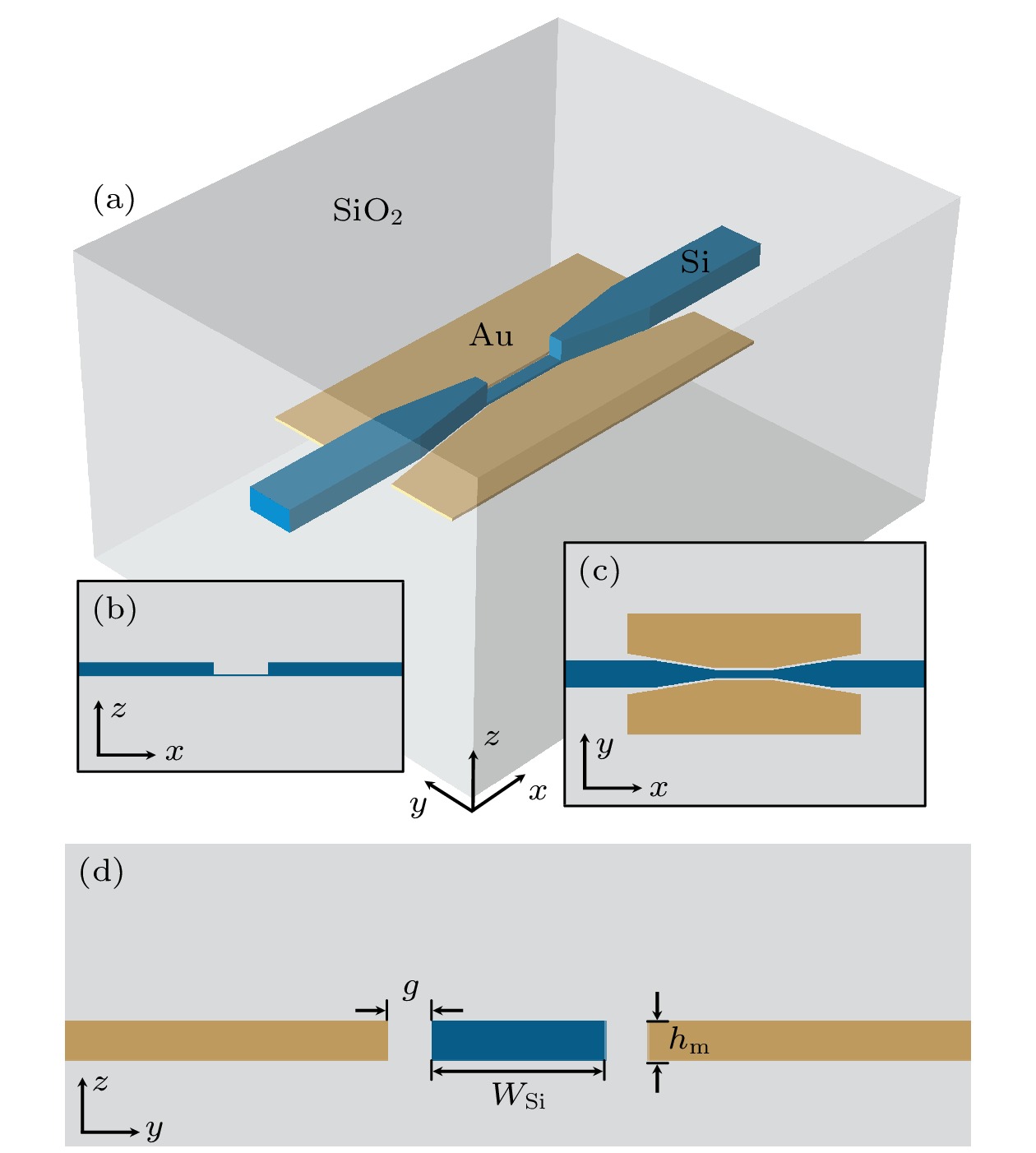
图 1 硅基混合表面等离激元光场窄化器件的结构示意图 (a) 三维图; (b) 侧视图; (c) 俯视图; (d) 中间处的截面图
Figure 1. Schematic of the proposed silicon hybrid plasmonic nanofocusing device: (a) 3D perspective view; (b) side view; (c) top view; (d) cross-sectional view at the center.
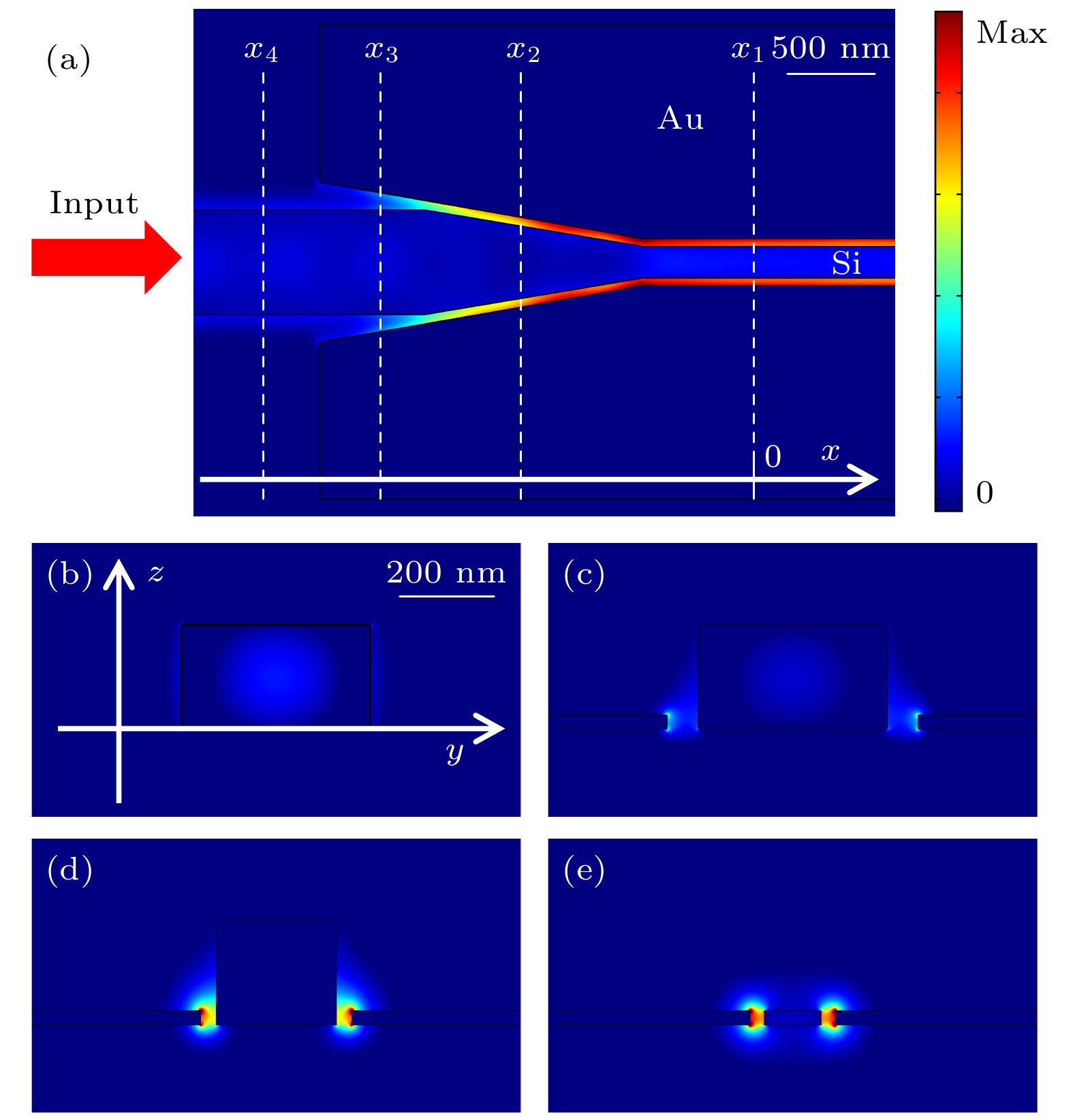
图 2 硅基混合表面等离激元光场窄化器件(WSi = 120 nm, g = 30 nm, hm = 30 nm)的光场分布图 (a) 整体俯视图; (b)—(e) 对应于x1 = 0 μm, x2 = –0.8 μm, x3 = –1.4 μm, x4 = –2 μm的截面图
Figure 2. Optical field distribution of the silicon hybrid plasmonic nanofocusing device (g = 30 nm, WSi = 450 nm, hm = 30 nm): (a) Overall top view; (b)–(e) cross-sectional view corresponding to x1 = 0 μm, x2 = –0.8 μm, x3 = –1.4 μm, x4 = –2 μm.
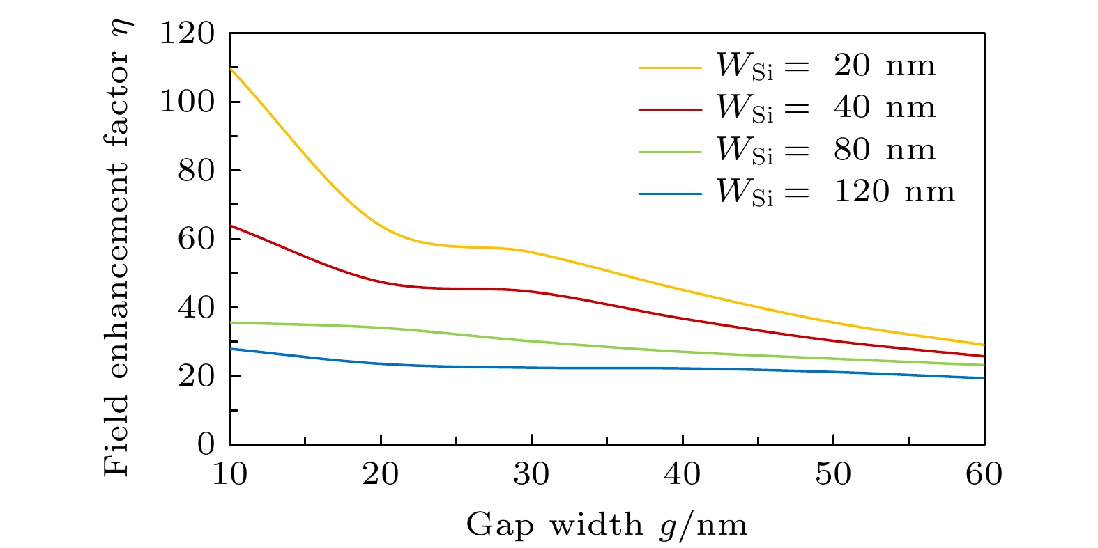
图 3 仿真计算的不同波导间隙的硅基混合表面等离激元光场窄化器件的场增强因子
Figure 3. Simulated field enhancement factor of the silicon hybrid plasmonic nanofocusing device with different gap width.

图 4 实验加工的硅基混合表面等离激元光场窄化器件(WSi = 120 nm, g = 30 nm, hm = 30 nm)的(a)光学显微镜图和(b) SEM图(伪彩上色)
Figure 4. (a) SEM image (false-colour) and (b) optical microscope image of the fabricated silicon hybrid plasmonic nanofocusing device (WSi = 120 nm, g = 30 nm, hm = 30 nm).

图 5 (a) 实验加工的硅基混合表面等离激元光场窄化器件的损耗谱线; (b) 不同间隙宽度g对应的损耗
Figure 5. (a) Experiment insertion loss spectra of the fabricated silicon hybrid plasmonic nanofocusing device; (b) gap width g dependence of insertion loss.

图 6 实验加工的不同波导间隙的硅基混合表面等离激元光场窄化器件的场增强因子
Figure 6. Field enhancement factor of the fabricated silicon hybrid plasmonic nanofocusing device with different gap width.
-
[1] Zhou Z, Yin B, Deng Q, Li X, Cui J 2015 Photonics Res. 3 B28
Google Scholar
[2] Zhou Z, Yin B, Michel J 2015 Light Sci. Appl. 4 e358
Google Scholar
[3] Dai D, Bowers J E 2014 Nanophotonics 3 283
Google Scholar
[4] Dai D, Bauters J, Bowers J E 2012 Light Sci. Appl. 1 e1
Google Scholar
[5] Zhou Z, Bai B, Liu L 2019 IEEE J. Sel. Topics Quantum Electron 25 4600413
Google Scholar
[6] Bai B, Yang F, Zhou Z 2019 Photonics Res. 7 289
Google Scholar
[7] Chen R, Bai B, Yang F, Zhou Z 2020 Optics Lett. 45 803
Google Scholar
[8] Chen R, Bai B, Zhou Z 2020 Photonics Res. 8 1197
Google Scholar
[9] Zhu K, Xu P, Sun P, Liu X, Li H, Zhou Z 2020 An Ultra-compact Broadband TE-pass Nanofocusing Structure (Beijing: Optical Society of America)
[10] Zhu K, Xu P, Sun P, Liu X, Li H, Zhou Z 2020 Low Loss, High Extinction Ratio Plasmonic Spot Size Converter (Beijing: Optical Society of America)
[11] Sun P F, Xu P F, Zhu K J, Zhou Z P 2021 Photonics 8 482
Google Scholar
[12] Gramotnev D K, Bozhevolnyi S I 2014 Nat. Photonics 8 13
Google Scholar
[13] Diaz F J, Li G, de Sterke C M, Kuhlmey B T, Palomba S 2016 J. Opt. Soc. Am. B 33 957
Google Scholar
[14] Diaz F J, Hatakeyama T, Rho J, Wang Y, O Brien K, Zhang X, Martijn De Sterke C, Kuhlmey B T, Palomba S 2016 Optics Express 24 545
Google Scholar
[15] Kim S, Lim Y, Kim H, Park J, Lee B 2008 Appl. Phys. Lett. 92 13103
Google Scholar
[16] Fu Y, Zhou W, Lim L E N, Du C L, Luo X G 2007 Appl. Phys. Lett. 91 61124
Google Scholar
[17] Mote R G, Yu S F, Ng B K, Zhou W, Lau S P 2008 Optics Express 16 9554
Google Scholar
[18] Shi H, Wang C, Du C, Luo X, Dong X, Gao H 2005 Optics Express 13 6815
Google Scholar
[19] Min C, Wang P, Jiao X, Deng Y, Ming H 2008 Appl. Phys. B 90 97
Google Scholar
[20] Stockman M I 2004 Phys. Rev. Lett. 93 137404
Google Scholar
[21] Babadjanyan A J, Margaryan N L, Nerkararyan K V 2000 J. Appl. Phys. 87 3785
Google Scholar
[22] Issa N A, Guckenberger R 2007 Plasmonics 2 31
Google Scholar
[23] Gramotnev D K, Vogel M W, Stockman M I 2008 J. Appl. Phys. 104 34311
Google Scholar
[24] Veronis G, Fan S 2007 Optics Express 15 1211
Google Scholar
[25] Chen L, Shakya J, Lipson M 2006 Optics Letters 31 2133
Google Scholar
[26] Ono M, Taniyama H, Xu H, Tsunekawa M, Kuramochi E, Nozaki K, Notomi M 2016 Optica 3 999
Google Scholar


 DownLoad:
Catalog
Metrics
- Abstract views: 2374
- PDF Downloads: 61
- Cited By: 0
