


-
With the increase of IGBT voltage and current ratings, the avalanche effect has become an important factor limiting the safe operating area (SOA) of the device. The hole injection of the p+n junction on the back of the device when the avalanche effect occurs is the main feature that distinguishes the avalanche effect of the IGBT from other devices. In this paper, the avalanche breakdown characteristics of IGBT and the behavior of avalanche-generated current filaments are studied through theoretical analysis and numerical simulation, and the physical mechanism dominating the behavior of avalanche-generated current filaments is revealed. The results show that the hole injection on the backside of IGBT leads to an additional negative differential resistance branch on the avalanche breakdown curve, and the strength of the negative differential resistance effect depends on the common base current gain of IGBT αpnp. With the increase of αpnp, the negative differential resistance effect becomes stronger, the avalanche current at the valley point where the additional negative differential resistance branch transforms into the positive differential resistance branch also becomes higher. And the valley point at the avalanche breakdown curve of IGBT dominates the strength of the avalanche-generated filament. As a result, the strength of avalanche-generated filament depends on the αpnp. With the lattice temperature increasing, the avalanche breakdown voltage of IGBT increases, leading to the shifting of the avalanche breakdown curve towards a higher voltage. And with the increase of αpnp, the offset of the avalanche breakdown curves at high and low temperature becomes smaller, which dominates the lateral movement speed of the avalanche-generated filament. With the increase of the αpnp and the decrease of the offset of avalanche breakdown curves at high and low temperature, the avalanche-generated filament laterally moves more slowly. To sum up, with the increase of the αpnp of IGBT, the avalanche-generated filament becomes stronger and moves more slowly, which extremely causes the local overheating where the filaments exist and lowers the avalanche robustness of the device. Therefore, the αpnp of IGBT must be controlled precisely in order to have a good trade-off between the characteristics and the reliability of IGBT.
-
Keywords:
- insulated gate bipolar transistor /
- avalanche effect /
- current filament /
- robustness
[1] Egawa H 1966 IEEE Trans. Electron. Devices 13 754
 Google Scholar
[2] Baburske R, Lutz J, Heinze B 2010 IEEE 2010 IEEE International Reliability Physics Symposium-Garden Grove (Anaheim) CA, USA, May 2–6, 2010 p162
[3] Hower P L, Reddi V K 2005 IEEE Trans. Electron. Devices 17 320
Google Scholar
[4] Schulze H J, Niedernostheide F J 2013 IEEE Trans. Electron. Devices 60 551
Google Scholar
[5] Knipper U, Wachutka G, Pfirsch F, et al. 2008 International Symposium on Power Semiconductor Devices & IC's Orlando, USA, May 18–22, 2008 p307
[6] Tong X, Liu S, Sun W, et al. 2020 IEEE Trans. Electron. Devices 67 3908
Google Scholar
[7] Endo K, Nakamae K 2019 IEEE Trans. Device Mater. Reliab. 19 723
Google Scholar
[8] Bhojani R, Kowalsky J, Lutz J, et al. 2018 International Symposium on Power Semiconductor Devices and IC’s Palmer House Hilton, USA, May 13–17, 2018 p164
[9] Lutz J, Baburske R, Chen M, et al. 2009 IEEE Trans. Electron. Devices 56 2825
Google Scholar
[10] Lutz J, Schlangenotto H, et al. 2018 Semiconductor Power Devices: Physics, Characteristic, Reliability (Switzerland: Springer International Publishing)
[11] Spirito P, Breglio G, Irace A, et al. 2014 IEEE Trans. Electron. Devices 61 1457
Google Scholar
[12] Baliga B J 2013 IEEE Trans. Electron. Devices 60 535
Google Scholar
[13] Heinze B, Felsl H P, Mauder A, et al. 2005 International Symposium on Power Semiconductor Devices & IC’s CA, USA, May 13–17, 2005 p159
[14] Wang C, Zhang L 2017 IEICE Electron. Express 14 1
Google Scholar
[15] Breglio G, Irace A, Napoli E, et al. 2013 IEEE Trans. Electron. Devices 60 563
Google Scholar
[16] Knipper U, Pfirsch F, Raker T, et al. 2008 International Conference on Advanced Semiconductor Devices and Microsystems Smolenice, Slovakia, Oct. 12–16, 2008 p159
[17] Felsl H P, Falck E, Niedernostheide F J, et al. 2006 International Symposium on Power Semiconductor Devices & IC’s Smolenice, Slovakia, June 4–8, 2006 p1
[18] Tong X, Liu S, Sun W, et al. 2020 Trans. Electron. Devices 67 3908
[19] Niedernostheide F J, Falck E, Schulze H J, et al. 2006 IEEP. Circ. Dev. Syst. 153 3
Google Scholar
[20] Shiba Y, Omura I, Tsukuda M 2016 28 th International Symposium on Power Semiconductor Devices & IC’s Prague, Czech Republic, June 12–16, 2016 p339
[21] Watanabe M, Shigyo N, Hoshii T, et al. 2019 International Symposium on Power Semiconductor Devices and IC’s Shanghai, China, May 19–23, 2019 p311
-

图 1 3.3 kV平面栅FS-IGBT的元胞剖面结构
Figure 1. 3.3 kV planar FS-IGBT structure.
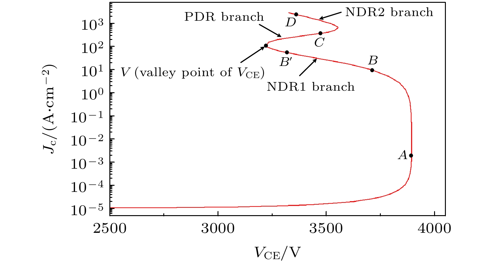
图 2 3.3 kV FS-IGBT的雪崩击穿特性曲线(T = 300 K, NP+ = 2×1017 cm–3, τp0 = 3 μs)
Figure 2. The simulated avalanche breakdown curve of 3.3 kV FS-IGBT(T = 300 K, NP+ = 2×1017 cm–3, τp0 = 3 μs).
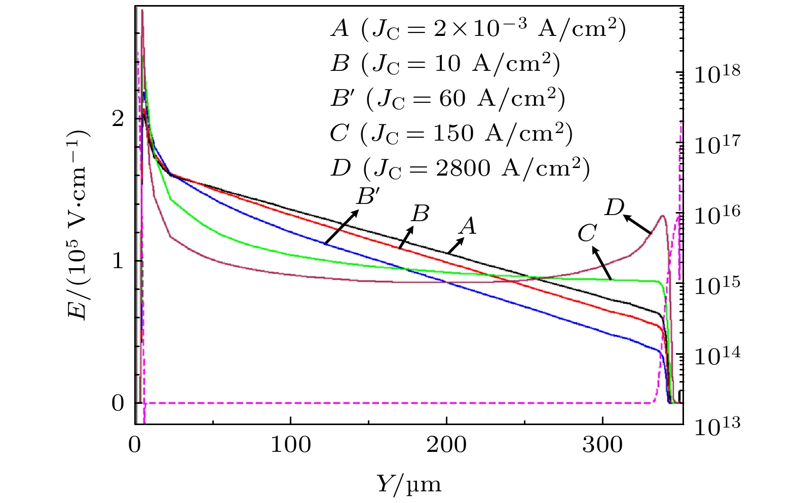
图 3 不同雪崩电流密度下器件内部的纵向电场分布(沿元胞中心剖分)
Figure 3. Vertical distributions of electric field along the cell center at different avalanche current(dissected along the cell center).
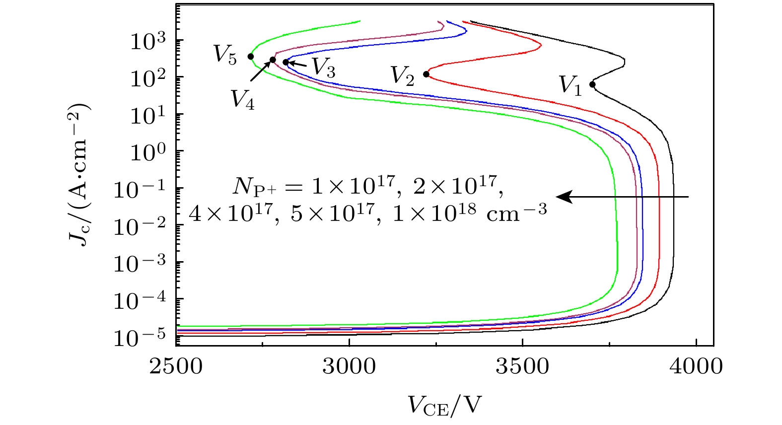
图 4 3.3 kV FS-IGBT在不同集电极掺杂浓度NP+下的雪崩击穿特性曲线(T = 300 K, τp0 = 3 μs)
Figure 4. The simulated avalanche breakdown curves of 3.3 kV FS-IGBT with different NP+(T = 300 K, τp0 = 3 μs)

图 5 3.3 kV FS-IGBT在不同集电极掺杂浓度NP+下, αpnp与雪崩电流密度JC的关系曲线
Figure 5. The αpnp for 3.3 kV FS-IGBT with different NP+ as a function of JC.

图 6 不同集电极掺杂浓度NP+的3.3 kV FS-IGBT在常温与高温下的雪崩击穿曲线(τp0 = 3 μs)
Figure 6. The avalanche breakdown curves of 3.3 kV FS-IGBT with different NP+ at high and low temperature (τp0 = 3 μs)

图 7 不同集电极掺杂浓度NP+的3.3 kV FS-IGBT在常温与高温下, αpnp与JC的关系曲线
Figure 7. The αpnp for 3.3 kV FS-IGBT with different NP+ as a function of JC at high and low temperature.

图 8 用于模拟雪崩电流丝的3.3 kV FS-IGBT结构模型(τp0 = 3 μs)
Figure 8. The structure model of 3.3 kV FS-IGBT (τp0 = 3 μs) used to simulate current filament at the static avalanche.
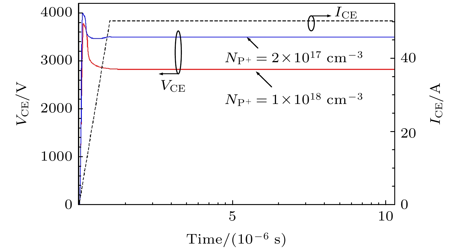
图 9 恒温仿真的NP+ = 2×1017 cm–3和NP+ = 1×1018 cm–3 FS-IGBT工作在静态雪崩模式下时, VCE随时间变化曲线(所施加的电流脉冲幅值为50 A, 上升时间1 μs)
Figure 9. Simulated VCE vs. time curve for FS-IGBTs with different NP+ working in static avalanche mode in isothermal case (the applied current pulse amplitude is 50 A, rise time is 1 μs).

图 10 恒温仿真的NP+ = 2×1017 cm–3和NP+ = 1×1018 cm–3 FS-IGBT工作在静态雪崩模式下时, 器件内部的电流密度分布(横向电流密度分布在J2结处被截取得到)
Figure 10. Simulated current density distributions inside the FS-IGBTs with different NP+ working in static avalanche mode in isothermal case (lateral current density distribution is along the J2 junction).

图 11 热电仿真的NP+ = 2×1017 cm–3和NP+ = 1×1018 cm–3 FS-IGBT工作在静态雪崩模式下时, VCE和最高晶格温度Tmax随时间变化曲线(所施加的电流脉冲与图9完全相同)
Figure 11. Simulated VCE and maximum lattice temperature Tmax vs. time curves for FS-IGBTs with different NP+ working in static avalanche mode in electrothermal case (applied current pulse is the same as Fig. 9).


图 12 热电仿真的NP+ = 2×1017 cm–3和NP+ = 1×1018 cm–3 FS-IGBT工作在静态雪崩模式下时, 器件内部的电流分布(横向电流密度分布在J2结处被截取得到)
Figure 12. Simulated current density distributions inside the FS-IGBTs with different NP+ working in static avalanche mode in electrothermal case (lateral current density distribution is along the J2 junction).
-
[1] Egawa H 1966 IEEE Trans. Electron. Devices 13 754
Google Scholar
[2] Baburske R, Lutz J, Heinze B 2010 IEEE 2010 IEEE International Reliability Physics Symposium-Garden Grove (Anaheim) CA, USA, May 2–6, 2010 p162
[3] Hower P L, Reddi V K 2005 IEEE Trans. Electron. Devices 17 320
Google Scholar
[4] Schulze H J, Niedernostheide F J 2013 IEEE Trans. Electron. Devices 60 551
Google Scholar
[5] Knipper U, Wachutka G, Pfirsch F, et al. 2008 International Symposium on Power Semiconductor Devices & IC's Orlando, USA, May 18–22, 2008 p307
[6] Tong X, Liu S, Sun W, et al. 2020 IEEE Trans. Electron. Devices 67 3908
Google Scholar
[7] Endo K, Nakamae K 2019 IEEE Trans. Device Mater. Reliab. 19 723
Google Scholar
[8] Bhojani R, Kowalsky J, Lutz J, et al. 2018 International Symposium on Power Semiconductor Devices and IC’s Palmer House Hilton, USA, May 13–17, 2018 p164
[9] Lutz J, Baburske R, Chen M, et al. 2009 IEEE Trans. Electron. Devices 56 2825
Google Scholar
[10] Lutz J, Schlangenotto H, et al. 2018 Semiconductor Power Devices: Physics, Characteristic, Reliability (Switzerland: Springer International Publishing)
[11] Spirito P, Breglio G, Irace A, et al. 2014 IEEE Trans. Electron. Devices 61 1457
Google Scholar
[12] Baliga B J 2013 IEEE Trans. Electron. Devices 60 535
Google Scholar
[13] Heinze B, Felsl H P, Mauder A, et al. 2005 International Symposium on Power Semiconductor Devices & IC’s CA, USA, May 13–17, 2005 p159
[14] Wang C, Zhang L 2017 IEICE Electron. Express 14 1
Google Scholar
[15] Breglio G, Irace A, Napoli E, et al. 2013 IEEE Trans. Electron. Devices 60 563
Google Scholar
[16] Knipper U, Pfirsch F, Raker T, et al. 2008 International Conference on Advanced Semiconductor Devices and Microsystems Smolenice, Slovakia, Oct. 12–16, 2008 p159
[17] Felsl H P, Falck E, Niedernostheide F J, et al. 2006 International Symposium on Power Semiconductor Devices & IC’s Smolenice, Slovakia, June 4–8, 2006 p1
[18] Tong X, Liu S, Sun W, et al. 2020 Trans. Electron. Devices 67 3908
[19] Niedernostheide F J, Falck E, Schulze H J, et al. 2006 IEEP. Circ. Dev. Syst. 153 3
Google Scholar
[20] Shiba Y, Omura I, Tsukuda M 2016 28 th International Symposium on Power Semiconductor Devices & IC’s Prague, Czech Republic, June 12–16, 2016 p339
[21] Watanabe M, Shigyo N, Hoshii T, et al. 2019 International Symposium on Power Semiconductor Devices and IC’s Shanghai, China, May 19–23, 2019 p311

 DownLoad:
Catalog
Metrics
- Abstract views: 2617
- PDF Downloads: 59
- Cited By: 0
