


Vol. 70, No. 17 (2021)
2021-09-05
INVITED REVIEW

INVITED REVIEW
2021, 70 (17): 177101.
doi: 10.7498/aps.70.20210626
Abstract +
The excited state dynamics is always an important and challenging problem in condensed matter physics. The dynamics of excited carriers can have different relaxation channels, in which the complicated interactions between different quasi-particles come into play collectively. To understand such ultrafast processes, the ab initio investigations are essential. Combining the real-time time-dependent density functional theory with fewest switches surface hopping scheme, we develop time-dependent ab initio nonadiabatic molecular dynamics (NAMD) code Hefei-NAMD to simulate the excited carrier dynamics in condensed matter systems. Using this method, we investigate the interfacial charge transfer dynamics, the electron–hole recombination dynamics, and the excited spin-polarized hole dynamics in different condensed matter systems. Moreover, we combine ab initio nonadiabatic molecular dynamics with GW plus real-time Bethe-Salpeter equation for the spin-resolved exciton dynamics. We use it to study the spin-valley exciton dynamics in MoS2. It provides a powerful tool for exciton dynamics in solid systems. The state-of-the-art NAMD studies provide a unique insight into a understanding of the ultrafast dynamics of the excited carriers in different condensed matter systems on an atomic scale.

YOUNG SCIENTISTS’ FORUM

YOUNG SCIENTISTS' FORUM
2021, 70 (17): 177301.
doi: 10.7498/aps.70.20210859
Abstract +
In recent years, two-dimensional transition metal chalcogenides (TMDCs) have been widely studied in the field of photodetection due to their excellent electronic and optical properties. Compared with the more reported field-effect transistor and heterojunction devices, homojunction devices have unique advantages in photodetection. This article focuses on the researches of photodetectors based on the homojunctions of TMDCs. First, the working principle of homojunction optoelectronic device is introduced. Then, the reported TMDCs based homojunctions are classified and summarized according to the adopted carrier modulation techniques. In addition, this article also specifically analyzes the transport process of photogenerated carriers in homojunction device, and explains why the lateral p-i-n homojunction exhibits fast photoresponse speed. Finally, the research progress of the TMDCs based homojunction photodetectors is summarized and the future development is also prospected.
REVIEW
2021, 70 (17): 178401.
doi: 10.7498/aps.70.20210316
Abstract +
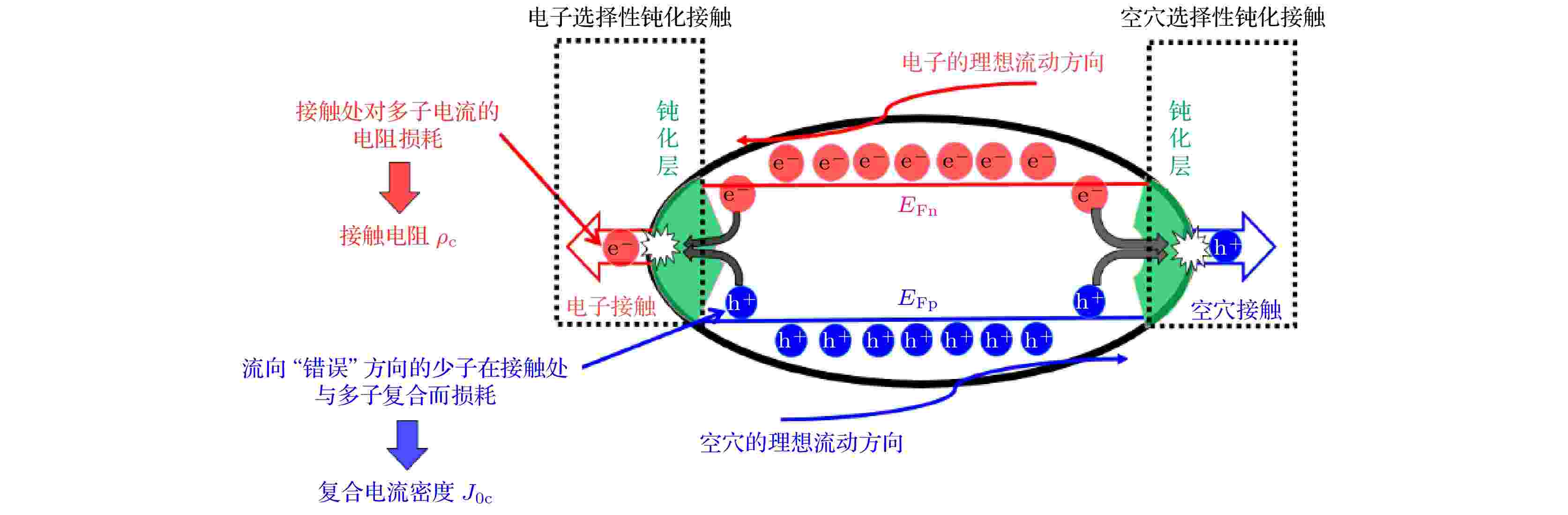
Current photovoltaic market is dominated by crystalline silicon (c-Si) solar modules and this status will last for next decades. Among all high-efficiency c-Si solar cells, the tunnel oxide passivated contact (TOPCon) solar cell has attracted much attention due to its excellent passivation and compatibility with the traditional c-Si solar cells. The so-called tunnel oxide passivated contact (TOPCon) consists of an ultra-thin silicon oxide layer less than 2 nm in thickness and a heavily doped poly-Si layer, which is used for implementing effective passivation and selective collection of carriers. This TOPCon solar cell has some advantages including no laser contact opening, no light-induced degradation and no elevated temperature-induced degradation because of N-type c-Si wafer, compatibility with high temperature sintering and technical scalability. This paper first introduces the basic structure and principles of TOPCon solar cells, then compares the existing methods of preparing ultra-thin silicon oxide layer and heavily doped poly-Si layer, and finally points out the future research direction of this cell based on the analysis of the current research status.
EDITOR'S SUGGESTION
2021, 70 (17): 178801.
doi: 10.7498/aps.70.20210180
Abstract +
GENERAL

COVER ARTICLE
2021, 70 (17): 170301.
doi: 10.7498/aps.70.20210512
Abstract +
The precise measurement of the infrared transition of hydrogen-deuterium (HD) molecule is used to test quantum electrodynamics and determine the proton-to-electron mass ratio. The saturated absorption spectrum of the R(1) line in the first overtone (2–0) band of HD molecule has been measured by the comb locked cavity ring-down spectroscopy (CRDS) method in Hefei [Tao L G, et al. 2018 Phys. Rev. Lett. 120 153001 ], and also by the noise-immune cavity-enhanced optical heterodyne molecular spectroscopy (NICE-OHMS) method in Amsterdam [Cozijn F M J, et al. 2018 Phys. Rev. Lett. 120 153002 ]. However, there is a significant difference between the line center positions obtained in these two studies. Later the discrepancy was found to be due to unexpected asymmetry in the line shape of the saturated absorption spectrum of the HD molecule. A possible reason is the superposition of multiple hyperfine splitting peaks in the saturated spectrum. However, this model strongly depends on the population transfer caused by intermolecular collisions, which is a lack of experimental and theoretical support. In this paper, the hyperfine structures of the ro-vibrational transition of HD are calculated in the coupled and uncoupled representations. The hyperfine structures of the R(0), P(1) and R(1) lines in the (2–0) band of HD molecule under different external magnetic fields are calculated. The corresponding spectral structures at a temperature of 10 K are simulated. The results show that the transition structure of HD molecule changes significantly with the externally applied magnetic field. The frequency shift of each hyperfine transition line also increases with the intensity of external magnetic field increasing. When the intensity of the external magnetic field is sufficiently high, the hyperfine lines are clearly divided into two branches, and they can be completely separated from each other. Because the dynamic effect of intermolecular collision and the energy level population transfer are very sensitive to the energy level structure, the comparison between experiment and theory will help us to analyze the mechanism of the observed special profiles. It will allow us to obtain accurate frequencies of these transitions, which can be used for testing the fundamental physics.

EDITOR'S SUGGESTION
2021, 70 (17): 170302.
doi: 10.7498/aps.70.20210262
Abstract +
Heavy ion collisions are an important method to study the quantum chromodynamics. In the early stage of relativistic heavy ion collisions, an extremely strong magnetic field is generated. The magnetic field will induce novel phenomena such as the chiral magnetic effect. However, the magnetic field will decrease rapidly, so it is difficult to measure its effect on the system. Charmonium states which are created by the initial scattering will be affected by the magnetic field and carry the information about it. We use the two-body Schrodinger equation with magnetic field to study the influence of the magnetic field on the charmonium state. The magnetic field is introduced via minimal coupling and its effect breaks the conservation of momentum and the conservation of angular momentum as well. The energy of the charmonium state depends not only on the magnetic field, but also on the momentum of the charmonium, thereby leading the final charmonium yield to be anisotropic. For a constant and homogeneous magnetic field, using the method of angular momentum expansion, we numerically calculate the energy spectra of the charm quark bound states with different magnetic field strengths and total momentum. The method is used to expand the three-dimensional wave function on the basis of different orbital angular momentum and spin states whose wave functions are numerically calculated first. In the actual calculation process, it is found that a good accuracy is achieved when taking $n\leqslant 2$ , $l\leqslant 7$ . Furthermore, the dependence of the Hamiltonian on the magnetic field and total momentum is analytically determined to be $H=H_0+(qB)^2 H_1+qBP_{{\rm{ps}},\perp} H_2$ . Therefore, only the coefficient matrices $H_{1}$ and $H_{2}$ need to be numerically calculated once and the Hamiltonian with arbitrary magnetic field and momentum can be determined. The inverse power method is then used to find the lowest eigenvalue in the angular momentum space. Such a numerical method significantly reduces the amount of calculation and still ensures the accuracy of the calculation as well. The calculation results show that as the magnetic field and the total momentum increase, the mass of the charm element increases. The increase of the mass can be as large as $20\%$ , when we take $eB = 20 m_{\rm{\pi}}^2$ and $P_{{\rm{ps}}}=1.8 \;{\rm{GeV }}$ , which can be easily achieved in RHIC collisions. Therefore there should exist significant magnetic effect on the $J/\psi$ production in heavy ion collisions.


2021, 70 (17): 170303.
doi: 10.7498/aps.70.20210432
Abstract +
The technology of generating Raman laser is not only an important research content in the field of quantum precision measurement, but also a core technology of quantum inertial sensors such as cold atom gravimeter, gyroscope. For 87Rb atoms, two 780-nm lasers with a frequency difference of 6.834 GHz and a stable phase are needed to generate Raman light. Raman lasers can be generated by optical phase-locked loops of two 780-nm narrow linewidth external cavity tunable semiconductor lasers (ECDL). But the system thus developed is complicated in structure and very poor in environmental adaptability. The other method to generate Raman laser is based on intracavity 1560-nm laser with frequency doubling and electro-optic modulation technology. This system is simple in structure and strong in environmental adaptability, but it will introduce sideband effects and cannot achieve phase lock due to the limit by the linewidth and feedback bandwidth performance of the laser. In view of this, based on two new 1560-nm external cavity lasers and a home-made phase-locked circuit, in this paper the phase lock of the laser is achieved, and a Raman laser with low phase noise is obtained. The phase noise of beat note signal is as low as –95 dBc/Hz at the Fourier frequency in a range from 1 kHz to 10 kHz. A comparison of this system with the phase-locked performance of the 780-nm dual laser and the hybrid dual laser shows that this scheme has a slight advantage. In addition, the effect of the phase-locking performance on the phase noise of the cold atom interferometer through the method of piecewise integration is analyzed in this work. The experimental results given in this work provide a scheme for developing a miniaturized Raman optical system suitable for external fields.

2021, 70 (17): 170304.
doi: 10.7498/aps.70.20210393
Abstract +
Superconducting Josephson junctions are the key devices for superconducting quantum computation and microwave single photon detection. It is important to fabricate the Josephson junctions with designable parameters. Different from the typical methods to calibrate the parameters of the Josephson junctions,, e.g., by using the microwave drivings and measuring the ratio of hysteresis current to critical one, in this paper we achieve the calibrations with the low frequency current biases. First, we measure the I-V characteristic curves of the fabricated Al/AlOx/Al junctions. Second, we measure the statistical distributions of the jump currents of the Josephson junction samples driven by the low frequency (@71.3 Hz) biased currents at an extremely low temperature of 50 mK. These two sets of experimental data are utilized to estimate the typical parameters of the Josephson junction, i.e., junction capacitance, critical current, and the damping coefficient, which are difficult to be directly measured in the usual experiments. The critical current and capacitance of the Josephson junction are estimated by fitting the statistical distribution of the measured jump currents with the relevant theoretical model of the "particle" escape from the potential driven by the thermal excitations and quantum tunnelings. With the calibrated critical current of the junction, the relation between $I/I_{\rm{c}}$ and ${\rm{d}}\varphi/{\rm{d}}\tau,\,\tau=\omega_{\rm{c}}t$ (with $\omega_{\rm{c}}$ being the plasmon frequency) is obtained from the measured $I\text-V$ curve. Using the standard resistively capacitance shunted junction model to fit such a relation, the damping coefficient of the junction can be estimated. With the estimated critical current, capacitance, and damping coefficient, the resistance $R_n$ of the junction at the working temperature is calibrated consequently. It is shown that our estimated results are in good agreement with that predicted by the famous Ambgaokar-Baratoff formula. Physically, the method demonstrated here possesses two advantages. First, it is relatively insensitive to the noise during the measurement of the junction's I-V characteristic curve, compared with the usual method to calibrate damping coefficient by measuring the ratio of hysteresis current to critical current. Second, only the low frequency driving is required to measure the jump current of the junction for estimating the damping coefficient. The microwave driving is not necessary. Hopefully, the present work is useful for the on-demand designs of the Josephson junctions for various applications.


2021, 70 (17): 170501.
doi: 10.7498/aps.70.20210208
Abstract +
Bursting is a complex multiple-time-scale nonlinear phenomenon in a nervous system and exhibits diverse patterns, which is modulated by the excitatory or inhibitory effect to achieve the physiological functions. According to the bifurcations of the fast subsystem, bursting is classified as different patterns including the mixed-mode bursting. Recently, many studies have found the paradoxical phenomena contrary to the common concept that the inhibitory effect induces the electrical activity to decrease or the excitatory effect induces the discharge activity to increase, which enriches the connotation of the nonlinear dynamics. To identify more examples of paradoxical phenomena of different bursting patterns and the underlying nonlinear mechanism, in the present study the paradoxical phenomena for the complex mixed-mode oscillations of the bursting pattern induced by the self-feedback mediated by both the inhibitory autapse and excitatory autapse and the bifurcation mechanism are acquired in the modified Morris-Lecar model. By using the fast/slow variable dissection method, the complex dynamics of the bursting is acquired, which is that the depolarization block behavior appears after the burst and before the quiescent state. The burst begins from a saddle-node bifurcation in an invariant cycle (SNIC) and terminates at a fold limit cycle (FLC) bifurcation. Furthermore, the FLC bifurcation is identified to play a key role in generating the paradoxical phenomenon. The inhibitory autapse induces the FLC bifurcation to shift leftward. However, the SNIC point remains unchanged. The change of FLC bifurcation point leads the parameter range of the burst to widen, the number of spikes per burst to become larger, and the average firing frequency to turn higher. Unlike the inhibitory autapse, the excitatory autapse induces the FLC bifurcation to shift rightward, and SNIC to be unchanged, thus reducing the bursting activity. Such results are different from those of the paradoxical phenomenon induced by the inhibitory autapse instead of excitatory autapse for the other bursting pattern and by the slow auatpse, which present a novel example and regulation mechanism of the paradoxical phenomena of the bursting patterns and show the diversity of the paradoxical phenomena, thus helping understand the potential functions of the bursting and self-feedback modulations of the brain neurons.

2021, 70 (17): 170502.
doi: 10.7498/aps.70.20210142
Abstract +
In the cerebral cortex, the large-scale synchronous firing of neurons can cause epilepsy, during which spiral waves can spontaneously occur. The relationship between the synchronous firing of a large number of neurons and the spontaneous generation of spiral waves is still unclear. In this paper, a two-dimensional neuronal network with the long-range coupling regions generated by adding long-range horizontal connections is constructed. The Morris-Lecar neuron model is used to study the propagation of waves in the two-dimensional neuronal network with the rectangular long-range coupling regions. Numerical simulation results show that the plan and target waves whose propagation directions are both parallel to that of the long-range coupling can lead the neurons to be excited synchronously in the long-range coupling region. This synchronous firing is accompanied by delayed firing of some neurons and premature firing of others. When the width of the long-range coupling region exceeds the critical width, all the neurons in the long-range coupling region delay firing. When the width of the long-range coupling region exceeds a maximum conduction width, the waves will not pass through the long-range coupling region. When the size of the rectangular region of the long-range coupling is selected appropriately, the synchronous excitation of neurons can cause network to present the backfiring effect and to have the selectivity of wave propagation direction. Furthermore, the selectivity of wave propagation direction is very sensitive to whether the neuron is in the stationary state and also to the change of coupling strength, so that the high frequency plane wave train can partially pass through the long-range coupling region whose width exceeds the maximum conduction width. So we can control whether the wave can pass through the long-range coupling region of a certain width by giving the neurons in the long-range coupling region a tiny perturbation. When one or two long-range coupling regions are constructed in the neural network and the size of the long-range coupling regions is selected appropriately, the self-sustaining plane wave, spiral wave and target wave can appear spontaneously in the network when the wave passes through the long-range coupling regions. The physical mechanisms behind those phenomena are also analyzed.

EDITOR'S SUGGESTION
2021, 70 (17): 170601.
doi: 10.7498/aps.70.20210462
Abstract +
There has been a great interest in quantum metrology (e.g., quantum interferometric radar) due to its applications in sub-Rayleigh ranging and remote sensing. Despite interferometric radar has received vast amount of attentions over the past two decades, very few researches has been conducted on another type of quantum radar: quantum illumination radar, or more precisely quantum target detection. It is, in general, used to interrogate whether the low-reflectivity target in a noisy thermal bath is existed using quantum light. The entanglement properties of its emitted light source give it a unique detection advantage over the classical radar. Entangled coherent state (ECS), as a class of quantum states with high entanglement robustness in noisy environments, has been widely used in several fields of quantum science such as quantum informatics, quantum metrology . In this paper, we investigate the target detection performance of quantum illumination radar based on three different types of ECS states. We employ the two-mode squeezed vacuum state (TMSV) and the coherent state as benchmarks to compare and analyze the relationship between the entanglement strength of the three types of ECS states and their quantum illumination detection performance. We found that the detection performance of the three ECS states is better than that of the coherent state. However, it is inferior to that of the TMSV state when the target is of low reflectivity. The emitted photon number is much smaller than the background noise (we call this as “good” illumination conditions). On the contrary, quantum illumination radar has no obvious advantage over coherent state radar for target detection under other illumination conditions; further, the detection performance of these three types of ECS states is not evidently related to that of the TMSV state and the coherent state. Finally, we reveal that the target detection performance of quantum illumination for the first two types of ECS states can be determined by their entanglement strength under “good” illumination conditions by adjusting the inter-modal phase of these two ECS states while keeping the emitted photon number constant. Under other illumination conditions, there is no evidence to demonstrate the entanglement strength of ECS states being associated with their target detection performance.

2021, 70 (17): 170602.
doi: 10.7498/aps.70.20210644
Abstract +

2021, 70 (17): 170701.
doi: 10.7498/aps.70.20210532
Abstract +
Trace gas analysis for SF6 decomposition is a powerful diagnostic method to identify partial discharge problem occurring in electrical equipment. In particular, it is recognized that the SF6 decomposition gases (such as CO, H2S, SO2 and CF4) can effectively determine the inner insulation condition of the electrical equipment. Currently, most of researches of diagnostic methods cannot meet the online high-precision detection of gas derivatives in SF6 electrical insulation equipment. Therefore, there is a need of developing a sensitive, selective and cost-effective sensor system for CO detection in an SF6 buffer gas environment due to the fact that the power system is filled with pure SF6 as the dielectric gas, which means that the concentration of SF6 is usually > 99.8%. The traditional photoacoustic CO gas sensors cannot be directly used in power system, since several SF6 physical constants strongly differ from those of N2 or air. In addition, SF6 molecule reveals uninterrupted and strong absorption lines in the mid-infrared spectral region. In this work, a CO gas sensor working in high concentration SF6 background gas is designed by using a distributed feedback (DFB) laser as an excitation source with a center wavelength of 2.3 μm. The absorption line strength of 2.3 μm is ~ two orders of magnitude higher than the absorption line strength around 1.56 μm, which can improve the sensor detection performance. A background-gas-induced high-Q differential photoacoustic cell is simulated numerically and tested experimentally. The quality factor of the designed photoacoustic cell in pure SF6 gas is 85, which is ~ 4 times higher than that in N2 carrier gas. The experimental results show that the maximum gas flow rate of the differential structure photoacoustic cell is ~ 6 times higher than that of the single resonant cavity photoacoustic cell. After optimizing the resonance frequency, gas velocity and working pressure of the sensor system, the detection sensitivity of the volume fraction of 1.85 × 10⁻⁶ is achieved. In the case of the volume fraction of 50 × 10–6 CO/SF6 gas mixture, the maximum photoacoustic signal amplitude of 19.6 μV is obtained, the corresponding normalized noise equivalent concentration (1σ) is 3.68 × 10⁻⁸ cm–1·W·Hz1/2 in 1 s integration time. A linear fitting is implemented to evaluate the response of the sensor from 50 × 10–6 to 1000 × 10–6, resulting in an R square value of 0.9997. The CO photoacoustic gas sensor has high sensitivity, good selectivity and strong noise immunity, which can provide an on-line detection technology for potential insulation fault diagnosis in the power system. The capability of CO gas sensor can be improved by using a higher excitation optical output power and/or reducing the PAC resonator volume to increase the cell constant.

2021, 70 (17): 170702.
doi: 10.7498/aps.70.20210464
Abstract +
Silicon pixel detectors are widely used as vertex detectors or inner trackers in high-energy collider experiments because of their excellent spatial resolution, extremely high counting capability and low power consumption. The study of the silicon pixel detector based on the monolithic active pixel sensor (MAPS) is one of the R&D schemes for upgrading the inner chamber of the Beijing spectrometer Ⅲ (BESⅢ) drift chamber (MDC). It is planned to build a 1/10 scale prototype of the inner chamber. The detector module is the basic component of the prototype, consisting of ten MIMOSA28 chips thinned to 50 μm, a flexible cable and a carbon fiber support. In order to study the performance of the module, a test system is set up. The system is composed mainly of five-layer modules, readout electronics and data acquisition system. This article focuses on the realization of the continuous data readout method with trigger marking function, the measurement of the noise level of the detector modules, the module response test by a radioactive source, and the study of the hit reconstruction algorithm. The test of trigger readout logic verifies the correctness of the continuous readout method with trigger marking. It can be concluded that analyzing consecutive three frames data (the previous frame, the current frame and the next frame) of each valid trigger will not lead to effective hit data loss. The noise level of the detector module is tested. The results show that the fixed pattern noise (FPN) is 0.253 mV, and the temporal noise (TN) is 1.65 mV. The fake hit rate is less than $ {10}^{-5} $ that can be ignored when the chip threshold is set to be above 4σ of noise. Two algorithms for hit reconstruction (i.e. adjacent method and comparison method) are studied and compared. When the average number of fired pixels caused by each hit is 2.562 and more than four hits in each frame of data, the adjacent method can find all of the fired pixels to be faster. During the test, the detector module and the electronics are proved to work well. These studies lay a foundation for further testing the performance of the detector prototype.


EDITOR'S SUGGESTION
2021, 70 (17): 170703.
doi: 10.7498/aps.70.20210482
Abstract +
Lead-bismuth (Pb-Bi) alloys, as a superconducting material, have been widely studied at their superconducting transition temperatures and the critical magnetic fields for different composition ratios. Most of experimental studies focused on the stable ε phase formed at high temperatures, but less on the Pb-Bi alloys grown at low temperatures. So far, the structural and superconducting properties of the low-temperature Pb-Bi phases are far from good understanding. Here, we report our investigation of structural and superconducting properties of a low-temperature phase of Pb-Bi alloy. The Pb-Bi alloy films with a nominal thickness of about 6 nm are prepared by co-depositing Bi and Pb on Bi(111)/Si(111)-(7 × 7) substrates at a low temperature of 100 K followed by annealing at a treatment of 200 K for 2 h. The structural and superconducting properties of the Pb-Bi alloy films are characterized in situ by using low-temperature scanning tunneling microscopy/spectroscopy (STM/STS). It is observed that the spatially separated phases of nearly pure Bi(111) domains and Pb1–xBix alloy domains are formed in the films, where these phases can be identified by their distinct differences in the atomic structure and the distributions of step heights in the atomically resolved STM images, as well as by their distinguished STS spectra. The Pb1–xBix alloy phase presents the structure of Pb(111), in which about x ≈ 0.1 Bi is substituted for Pb. The STS spectra show that the Pb1–xBix alloy phase is superconducting, with a transition temperature Tc = 7.77 K derived from the variable-temperature measurements. This transition temperature is higher than that in pure Pb film (6.0–6.5 K), which can be well explained by the Mattias rules, with considering the fact that the average number of valance electrons increases after Bi atoms with five valance-electrons have been substituted for Pb atoms with four valance-electrons. The analysis shows that the ratio $ 2\Delta (0)/{k_{\rm{B}}}{T_{\rm{C}}}$ is about 4.94 with the superconducting gap $ \varDelta (0) = 1.66$ meV at 0 K, indicating that the Pb1–xBix alloy is a strongly-coupled superconductor. The non-superconducting Bi(111) and the superconducting Pb1–xBix alloy domains form an in-plane superconductor-normal metal-superconductor (S-N-S) Josephson junction. The proximity effect in the Bi(111) domains is measured at different N-S junctions, which suggests that the lateral superconducting penetration length in Bi(111) might be affected by the area of the quasi-two-dimensional interface. The superconducting gap in the Bi(111) region with a narrow width of 23 nm in an S-N-S Josephson junction is found to be greatly enhanced due to the existence of multiple Andreev reflections. Since Bi can host potential topological properties, the lateral Bi(111)-Pb1–xBix heterostructures, because of the existing proximity effect, could have potential applications in exploring the novel topological and superconducting phenomena.


NUCLEAR PHYSICS
2021, 70 (17): 172401.
doi: 10.7498/aps.70.20210303
Abstract +
Indium phosphide (InP) has the characteristics of high electron mobility, large band gap, high temperature resistance, and radiation resistance. It is an important material of electronic devices in the space radiation environment. With the miniaturization of electronic devices, the displacement damage (DD) effect caused by a single heavy ion in the device may give rise to permanent failure. Therefore, this paper uses Monte Carlo software Geant4 to simulate the transportation process of space heavy ions(C, N, O, Fe) in InP. The non-ionizing energy loss (NIEL) of heavy ions is calculated for getting the information about displacement damage. Some conclusions are drawn as follows. 1) NIEL is proportional to the square of the atomic number, which means that single Fe can make severe displacement damage in InP. 2) The heavy ions NIEL is 3 to 4 orders of magnitude larger than PKA NIEL. The NIEL is proportional to the non-ionizing damage energy of recoil atoms produced by nuclear elastic collision, which indicates that the primary recoil atoms produced by heavy ions are the main cause of InP DD. 3) The number of heavy ions in space is small, so the proportion of total non-ionizing damage energy produced by heavy ions in 0.0125 mm3 InP is only 2.56% in one year. But the NIEL of heavy ions NIEL is 2–30 times that of protons and α particles, so the DD effect caused by single heavy ion incident on InP electronic device still needs to be considered. 4) NIEL decreases slightly with the increase of material thickness. The reason is that low-energy heavy ions are completely deposited in the front of InP, resulting in a non-uniform distribution of non-ionizing energy deposited in the material. Analyzing the dependence of mean DD energy with depth, we find that mean DD energy decreases with incident depth increasing, which means that the most severe DD region of heavy ions in InP is in the front of material.
ATOMIC AND MOLECULAR PHYSICS
EDITOR'S SUGGESTION
2021, 70 (17): 173201.
doi: 10.7498/aps.70.20210181
Abstract +
Based on the nondegenerate perturbation theory, the Stark-induced transitions are studied for hydrogen-like isoelectronic sequences (Z = 1–92). The Stark-induced mixing coefficients and transition probabilities between the 2s1/2-1s1/2 levels of hydrogen-like ions are reported. The trend of Stark-induced transition probabilities varying with atomic number Z between 2s1/2-1s1/2 levels of hydrogen-like ions and the relativistic effect on the Stark-induced mixing coefficients and transition probabilities are discussed. The scaling relations of the nonrelativistic and relativistic Stark-induced transition probabilities with atomic number Z are obtained. The results show that the Stark-induced transition probabilities of hydrogen-like ions decrease monotonically along the isoelectronic sequence with the increase of atomic number Z. In addition, the relativistic effect reduces the Stark-induced transition probabilities of hydrogen-like ions, for example, by about 55% at Z = 92.
ELECTROMAGNETISM, OPTICS, ACOUSTICS, HEAT TRANSFER, CLASSICAL MECHANICS, AND FLUID DYNAMICS

2021, 70 (17): 174201.
doi: 10.7498/aps.70.20210184
Abstract +
Single-photon detectors based on avalanche photodiodes and time-correlated single-photon counting technology are widely used in pulsed laser ranging. The ranging accuracy is one of the most important performances of laser ranging. In this work, a laser ranging method based on high-precision single-photon detector is developed to achieve laser ranging for non-cooperative targets with hundred-micron-level ranging accuracy. In the system, a low-time jitter Si APD single photon detector, picosecond pulsed laser and high-precision timing counter are used to reduce the time jitter of the ranging system, and a reference position is added to suppress the influence of delay drift of the system. And a laser interferometer system with a ranging resolution of 1 nm and an accuracy of 0.5 ppm is used to calibrate the distance of each movement of the ranging target. The photon flight time accuracy of 0.5 ps is achieved while the integral time ≥ 3 s. The ranging accuracy of 65 μm@RMS is realized, while the target is 2 m away. This work is one of the highest levels of pulsed time-of-flight ranging, and provides an effective technology for high-precision ranging and imaging of long-range non-cooperative targets.

2021, 70 (17): 174301.
doi: 10.7498/aps.70.20210111
Abstract +
An annular groove (AG) structure with depth gradient is proposed which can manipulate the spatial distribution of the acoustic scattering field for a finite rigid cylinder in water. An analytical analysis is given for better understanding the underlying mechanism of the abnormal scattered wave, which can be accomplished by using the phased array theory. When the plane acoustic wave is normally incident, the scattering acoustic wave in the transverse direction of the cylinder deflects, which is due to the interaction between the phase delay modulated by the AG structure with varying groove depths and the Bragg scattering of adjacent grooves. The finite element method is used to calculate the acoustic scattering field of a finite rigid cylinder with annular grooves and obtain the frequency and spatial distribution characteristics. How the structural parameters such as depth, gradient, and duty ratio of the annular grooves affect the acoustic scattering field is discussed in detail. The results show that the target strength in the transverse direction decreases linearly with duty ratio increasing while the target strength in the deflection direction of the acoustic wave increases with the duty ratio until δ = 30%, after which it remains almost constant. When the incident acoustic wave is fixed, the acoustic scattering wave of the AG cylinder can be deflected by designing the gradient appropriately, and the deflection direction is independent of the frequency. Numerical and experimental results for a cylinder with multiple annular-groove units show that the spatial directivity of the scattering field of the grooved cylinder changes, and the target strength is enhanced at six pre-designed deflection angles. Meanwhile, the deflected acoustic wave has a certain width and the interference among periodic structures of the AG units exists, which makes the spatial directivity of the scattering field of the cylinder equalize and changes the scattering characteristics of the cylinder, thereby providing a theoretical basis for designing three-dimensional underwater objects each with an acoustic stealth.
2021, 70 (17): 174302.
doi: 10.7498/aps.70.20210495
Abstract +
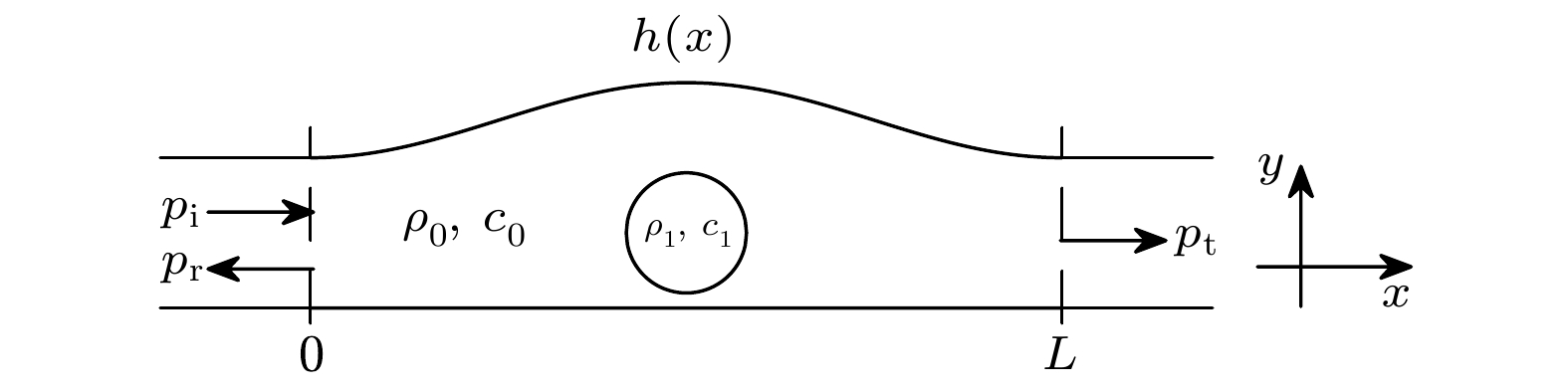
Inhomogeneity in a medium will cause wave scattering, influencing the transfer of energy or information. However, it is possible to prepare a prescribed wavefront which propagates through an inhomogeneous medium with unity flux-transmittance. This phenomenon is first predicted in the context of mesoscopic electron transport. Another remarkable phenomenon is the bimodal distribution of the transmission singular values, which implies that in a lossless medium the full solution space in the scattering region can be spanned only by open channels, which are completely transmitted, and closed channels, which are completely reflected. In mesoscopic physics, random-matrix theory is usually utilized to deal with the statistical properties of matrices with randomly distributed entries since the medium is assumed to be randomly fluctuating. In this paper, we propose a method of systematically studying the maximal flux transmission through an inhomogeneous acoustic waveguide. The model is chosen to be a waveguide with varying cross-sections and a penetrable scatterer, and the method is based on the coupled mode theory. This method can be used to analyze the frequency of nearly complete transmission for an arbitrary incident wave, and to analyze the incident wave that is able to generate the maximal flux-transmittance for any given frequency. We construct the transmission matrix and the horizontal wavenumber matrix by using orthonormal basis functions, and give the expression of flux-transmittance. Then the optimal incident wave which brings the maximal transmittance through the scattering region is derived based on singular value decomposition. The optimal incident waves are independent of the evanescent modes since evanescent modes do not transfer any energy. But the evanescent modes can give rise to the multivaluedness of wave solutions with complete flux transmission. Considering the fact that acoustic waveguides can naturally resist the influence of highly oscillating perturbations since most of them correspond to evanescent modes), the maximal flux transmission in waveguide is thus found to be highly robust. Especially at a specific frequency, the complete wave transmission has perfect robustness. This proposed method can be generalized to any other frequency, to other types of scatterers, or to other kinds of boundary conditions, and can provide guidance in designing acoustic metamaterials and in highly efficient communication.

2021, 70 (17): 174303.
doi: 10.7498/aps.70.20210404
Abstract +
For the reverberation experiments with a near surface source or receiver, surface reverberation arriving first after source signal is not influenced by bottom reverberation due to time-delay difference of acoustic multipath in deep water. A surface reverberation model is proposed in the paper. The Green’s function of sound propagation is described by the ray theory, and first-order small-slope approximation is employed for the surface scattering from full angle. The effect of bubbles scattering is also considered to get the surface reverberation theory. The reverberation model is verified by comparing the simulation results with the experimental data. The measured data show that the decaying rate of surface reverberation intensity decreases with the frequency increasing. Numerical calculation demonstrates that the frequency dependence is caused by the positive correlation between scattering strength and frequency, and the surface reverberation at low frequency for low sea state is dominated by the scattering from rough air-sea interface. Moreover, the reverberation data from experiment show that the surface reverberation is not sensitive to the change of receiving depth. A method of inversion for the two surface-wave spectral parameters in the model is achieved based on the reverberation model. The inversion results verify that the spectral parameters of rough surface can be obtained from surface reverberation data on the premise of the wind speed parameter. As a result, the scattering properties of rough interface will be obtained.

2021, 70 (17): 174304.
doi: 10.7498/aps.70.20210149
Abstract +
The performance of the method of measuring the time-correlated single photon counting signal is the key to improving the ranging accuracy of single photon light detection and ranging (LiDAR) technique, where noise elimination is a critically essential step to obtain the characteristics of signal. In this paper, a new method called elastic variational mode extraction (EVME) is proposed to extract the feature of the reflected photons from noisy environment. The method takes into account the characteristic of photon counting signal, and improves variational mode decomposition (VMD) method by adopting a new assumption that the extractive mode signal should be compact around desired center frequency. The proposed method also uses the elastic net regularization to solve ill-posed problem instead of Tikhonov regularization mentioned in VMD. Elastic net regularization takes into account both L2-norm regularization and L1-norm regularization, which can add an extra analysis dimension compared with the Tikhonov regularization. The method is validated with real data which are acquired on condition that average transmitting power is 25 nW while the average background noise power is 19.51 μW. The root mean square error of the reconstruction accuracy reaches 1.414 ns. Furthermore, compared with VMD, Haar wavelet, Hibert envelope, empirical mode decomposition (EMD) and complete ensemble empirical mode decomposition method based on adaptive noise (CEEMDAN) under different conditions, the proposed method show fast and stable performance under an extreme case.

2021, 70 (17): 174305.
doi: 10.7498/aps.70.20210119
Abstract +
In order to improve the computational efficiency of algorithms while exploring the method to overcome the ambiguity problems in underwater geo-acoustic inversion, we use the data of transmission losses at the broadband sound frequencies and multiple propagating distances with the matrix of polynomial chaos expansion coefficients of transmission losses to invert the speed (c), attenuation (α) of compression sound wave and the density ratio of seabed to seawater (ρ) in their prior searching intervals. When approximating the transmission loss with the polynomial chaos expansion, the expansion coefficients are the functions of parameters including sound frequency, source and hydrophone’s position while the polynomial bases are functions of the above geo-acoustic parameters which are uniformly distributed in their respective intervals. The expansion coefficients are calculated by embedding the orthogonal polynomial bases into the acoustic wide-angle parabolic equation model. After that, the coefficients are deduced using the Galerkin projection and least angel regression. Under the situations of low sound frequency, short or medium sound propagation distance and short or medium length of intervals of geo-acoustic parameters, the polynomial chaos expansion can approximate the transmission losses accurately with the relatively error less than 1%. In the simulation case, with the high signal to noise ratio and the low errors of relative distances between source and receivers, the geo-acoustic parameters can be inverted accurately when the appropriate truncated powers are chosen. And the time cost is reduced by at least an order of magnitude compared with that of traversal grids searching procedure.
PHYSICS OF GASES, PLASMAS, AND ELECTRIC DISCHARGES

2021, 70 (17): 175201.
doi: 10.7498/aps.70.20210241
Abstract +
Photonic crystals are widely used in a class of narrow-band frequency selective filter due to their excellent ability to control electromagnetic waves, in which the working frequency depends on the structural parameters of the point defect resonant cavity of the photonic crystal, and the introduction of some dispersive media into the cavity makes the filter adjustable. In general, this kind of cavity-filter is very sensitive to the parameter disturbance of the cavity, and the quality factor of the filter can be reduced significantly by material loss. On the other hand, some studies have shown that there may be bound states at the interface between two different photonic crystals, and the bound state is often accompanied by narrow band and high transmittance, which implies that a narrow-band filter based on bound states is feasible. Importantly, filters based on bound states may be resistant to material loss to some degree. In this paper, a bound state related tunable narrow-band filter composed of a one-dimensional photonic crystal and a two-dimensional plasma photonic crystal is proposed, and the working frequency of the filter is located in the common band gap of the two photonic crystals. The COMSOL Multiphysics finite element simulation software is used to study the influences of geometric parameters of the one-dimensional photonic crystal and plasma parameters on the performance of the filter. It is found that the closer to each other the center frequencies and depths of the two different forbidden bands are, the greater the peak transmittance of the filter, in which the center frequency dominates, will be. On the other hand, the working frequency of the filter is directly proportional to plasma density and inversely proportional to collision frequency. The quality factor of the filter first increases and then decreases with the increase of plasma density, and decreases with the increase of collision frequency. The peak transmittance of the filter first increases and then decreases with the increase of plasma density, and decreases with the increase of plasma collision frequency. Finally, with the increase of collision frequency, both the peak transmittance and the quality factor decrease slightly, which indicates that the filter has a certain resistance to plasma loss. We believe that this work is helpful in investigating some new plasmonic photonic crystal filters.
CONDENSED MATTER: STRUCTURAL, MECHANICAL, AND THERMAL PROPERTIES

2021, 70 (17): 176201.
doi: 10.7498/aps.70.20210414
Abstract +
Based on the electromagnetic loading device CQ-4, an experimental method of simultaneously measuring the refractive index and high pressure sound velocity of transparent material is established. The ramp wave compression experiment of PMMA is carried out under a pressure of 14 GPa. The velocity history curves of PMMA sample rear surface are obtained by dual laser heterodyne velocimetry (DLHV). The velocity curve shows obvious double wave structure, which indicates the elastic-plastic transition. The refractive index particle velocity optical characteristics and Lagrangian sound velocity particle velocity dynamic characteristics of PMMA are obtained simultaneously with the experimental data processing.
CONDENSED MATTER: ELECTRONIC STRUCTURE, ELECTRICAL, MAGNETIC, AND OPTICAL PROPERTIES

2021, 70 (17): 177201.
doi: 10.7498/aps.70.20202223
Abstract +
This paper studies the changes in electronic transport properties caused by InGaN as an AlGaN/GaN insertion layer, and considers the effects of the spontaneous polarization and piezoelectric polarization of AlGaN and InGaN barrier layers on the surface density of polarized charge, and the concentration of two-dimensional electron gas (2DEG) in AlxGa1–xN/InyGa1–yN/GaN double heterojunction high-electron-mobility transistor. The InGaN thickness and interface roughness scattering, random dipole scattering and polar optical phonons under different In molar compositions are analyzed. The calculation results show that the interface roughness scattering and random dipole scattering have an important influence on the electron transport properties of the double heterojunction AlxGa1–xN/InyGa1–yN/GaN, and the polar optical phonon scattering has the weakest influence; 2DEG concentration, the strength of interface roughness scattering, random dipole scattering and polar optical phonon scattering are determined by the thickness of the InGaN barrier layer and the molar composition of In. This paper takes 2DEG in the AlxGa1–xN/InyGa1–yN/GaN double heterojunction as the research object, considering the barrier layer of finite thickness, taking into account the spontaneous polarization effect and piezoelectric polarization effect of each layer, and giving AlxGa1–xN/GaN 2DEG characteristics in the InyGa1–yN/GaN double heterostructure, discussing the scattering of 2DEG concentration and interface roughness by changing the In molar composition and the thickness of the InGaN barrier layer under the same Al molar composition and the thickness of the AlGaN barrier layer, Random dipole scattering and polar optical phonon scattering. The results of the present study are of great significance in controlling the 2DEG concentration in the AlxGa1–xN/InyGa1–yN/GaN double heterojunction structure and improving the electron mobility. This paper presents the analytical expression of 2DEG concentration ns in AlxGa1–xN/InyGa1–yN/ GaN double heterostructure. The effects of the thickness of the InGaN insertion layer and the molar composition of indium on the 2DEG concentration, interface roughness scattering, random dipole scattering and total mobility are studied. According to the theoretical calculation results, on condition that the physical properties of the AlGaN barrier layer remain unchanged, choosing the appropriate InGaN barrier layer thickness and In molar composition concentration can better control the 2DEG concentration and carrier mobility. These results are beneficial to widely using the double heterojunction AlxGa1–xN/InyGa1–yN/GaN in actual nitride based semiconductor devices.

2021, 70 (17): 177601.
doi: 10.7498/aps.70.20210336
Abstract +
Bimetallic core-shell nanoparticles such as NiCu are of great interest not only due to their excellent stability, selectivity, and magnetic and catalytic properties, but also because they are tunable by changing the morphology, surface element distribution, and particle size of the nanoparticles. The surface segregation and structural features of NiCu bimetallic nanoparticles, the deposition growth and the surface diffusion of Cu adsorbed atoms on the Ni substrate surface are studied by using molecular dynamics and the Montero method combined with embedded atomic potential. The results show that the Cu atom has a strong tendency of surface segregation. With the increase of concentration of Cu atoms, Cu atoms preferentially occupy the vertex, edge, (100), and (111) facet of nanoparticles due to the difference in configuration energy between Cu atoms and surface Ni atoms with different coordination numbers after the exchange, and finally form perfect Ni-core/Cu-shell nanoparticles. When growth temperature T = 400 K, the Ni-core/Cu-shell structure formed is the most stable. By observing the NiCu core-shell structure’s growth sequence, it is found that a few Ni atoms are replaced by Cu atoms on the step edge of the Ni substrate. The diffusion energy barrier of Cu atoms adsorbed on a Ni substrate surface is calculated by using the nudged elastic band method. The results show that Cu atoms adsorbed need to overcome a large ES barrier for both exchange and diffusion, making it difficult to diffuse between the facets of Ni substrate surface in a temperature range of 200–800 K. The lowest energy barrier for the diffusion of Cu atoms between facets of Ni substrate surface is 0.43 eV, and the diffusion path is from (111) facet to (100) facet. In contrast to Ni substrate, Ni atoms deposited on Cu substrate can easily migrate from the (111) facet to the (100) facet with a diffusion energy barrier of only about 0.12 eV, and at the present simulated temperature, Ni adsorbed atoms are unable to migrate on the (100) facet, resulting in a growth configuration toward an octahedral shape with its eight apex angles almost occupied by Ni atoms. In this paper, a new idea and method are provided for the preliminary design of NiCu nano-catalysts from atoms.

2021, 70 (17): 177801.
doi: 10.7498/aps.70.20210493
Abstract +

INTERDISCIPLINARY PHYSICS AND RELATED AREAS OF SCIENCE AND TECHNOLOGY

2021, 70 (17): 178101.
doi: 10.7498/aps.70.20210341
Abstract +
First-principles calculation and experimental methods are used to study the interfacial properties and reaction of diamond/Al composites. Based on the first-principles method, the interfacial adhesion work (Wad), electronic structure and charge transfer of diamond/Al models are calculated systematically. The results show that the adhesion work of diamond(100)/Al(111) is 41% higher than that of diamond(111)/Al(111), therefore, the interface bonding of diamond(100)/Al(111) interface is stronger. According to the analysis of the electronic structure, there are more charges transferring at the diamond(100)/Al(111) interface, and the high charge density is distributed on the side of C atoms. The redistribution of charges at the interface is conducive to the formation of Al—C bond, so that the tendency of forming Al—C bonds is greater. The introduction of Al—C bond can promote the formation of C—C bond at the diamond(100)/Al(111) interface and improve the interfacial adhesion work. In addition, the diamond/Al composites are fabricated by vacuum gas pressure infiltration, and multi-scale characterization of the interface structure of diamond/Al composites is carried out. The interfacial debonding occurs mainly on the diamond {111}. Meanwhile, the interface product Al4C3 is easier to form on the diamond {100}. The experimental phenomenon is consistent with the calculated results. Moreover, the influence of the interfacial reaction on the properties and stability of diamond/Al composites are further discussed through heat-moisture treatment. The study finds that the performance degradation in heat-moisture environment is related mainly to the hydrolysis of the interface product Al4C3. After 60 days’ heat-moisture, the thermal conductivity of the diamond/Al composites decreases by 29.9%, and the bending strength is reduced by 40.1%. The large attenuation of performance is not conducive to the stability of composites in complex environments. Therefore, inhibiting the formation of Al4C3 and improving interfacial selectivity are of great importance in developing the performance and stability of diamond/Al composites. The research in this paper not only lays a theoretical foundation for the first-principles calculation of the interface properties of diamond/metal, but also possesses important guidance significance in designing the diamond/metal composites.

EDITOR'S SUGGESTION
2021, 70 (17): 178102.
doi: 10.7498/aps.70.20210344
Abstract +
Programmable metasurfaces incorporating with tunable materials or components are emerging as an attractive option to realize reconfigurable manipulations of electromagnetic (EM) behaviors in real-time. Many efforts have been devoted to the realization of active EM manipulations of the metasurface and significant progress has been achieved, showing their unprecedented ability to arbitrarily manipulate wavefronts in dynamic functions. However, most of the existing multi-beam metasurfaces are based on passive building blocks, only possessing one or a few functions, which cannot provide tunable and independent multi-beam control, thus limiting their further uses in wireless communications. Hence, a 1-bit coding metasurface with high-efficiency, programmable, and independent multi-beam control is proposed in this paper, providing dynamic EM responses with real-time reconfigurability, and controlled by external digital circuits through direct current (DC) bias networks. Specifically, the meta-atom loaded with PIN diodes is employed to achieve independently tunable phase characteristics, thus complex EM functions can be manipulated by redistributing the spatial phases of the metasurface. Symmetric/asymmetric independent dual- and multi-beam manipulations are analyzed theoretically and simulated by EM software. Then as an experimental verification, a metasurface consisting of 14 × 14 meta-atoms is fabricated and tested in a standard microwave anechoic chamber, and the measured results accord well with the simulations. The proposed metasurface has promising ability to generate the arbitrary and independent multi-beams, which may largely enhance the information capacity of the metasurfaces, offering untapped potentials in wireless communication systems.

2021, 70 (17): 178201.
doi: 10.7498/aps.70.20210455
Abstract +
Silicon is considered as a first candidate for ideal anode material of the next-generation lithium-ion battery due to its high theoretical capacity to meet the demand for higher energy density. On the other hand, high theoretical capacity is accompanied by massive volume expansion, which gives arise to high stress and crack and pulverization of anode particles. Finally, the capacity of the battery fades gradually. While some kinds of factors contribute to the failure of silicon-based electrodes, the most important one is the diffusion-induced stress generated in silicon-based electrode particles. The cyclic processes of lithiation and delithiation are accomplished by the intercalation into and deintercalation from the silicon particles of lithium ions. During the cycle, physical processes and chemical processes, such as diffusion of lithium ions, phase transition, and volume expansion, take place simultaneously, making the cyclic process a strong-coupling problem to be addressed. For example, the intercalation of lithium ions into the electrode results in volume expansion and phase transition of anodes, thereby inducing stress; in turn, stress affects the diffusion process of lithium ions. Aiming to probe this problem, with the finite deformation hypothesis, an electrochemical-mechanical coupling model is used to study the variation and distribution of concentration and stress of core-shell structure during lithiation. And more importantly, great emphasis is put on the optimal design of core-shell structure. The numerical results show that the shell is useful in prohibiting the volume expansion of silicon core, but large compressive radial stress in silicon core may cause the core and shell to be detached, while the tangential tensile stress at the core-shell interface leads the shell to fracture. To improve the electrochemical and mechanical performance and hence lengthen the cycle life of lithium-ion batteries, two kinds of optimal designs are considered: 1) single-layered core-shell structure and 2) double-layered core-shell structure. The numerical results suggest that the softer shell material is suitable for a single-layered core-shell structure and the inner-soft & outer-hard design is optimal for the double-layered core-shell structure. Furthermore, the effects of Young's modulus of the inner and outer carbon layer materials on the chemical and mechanical performance of anode are explored. The simulation shows that the optimal Young's modulus of the inner shell is less than 10 GPa, and that of the outer shell is not higher than 70 GPa. This research is helpful in designing and optimizing the silicon-based anode electrodes of lithium-ion batteries.
2021, 70 (17): 178501.
doi: 10.7498/aps.70.20210467
Abstract +
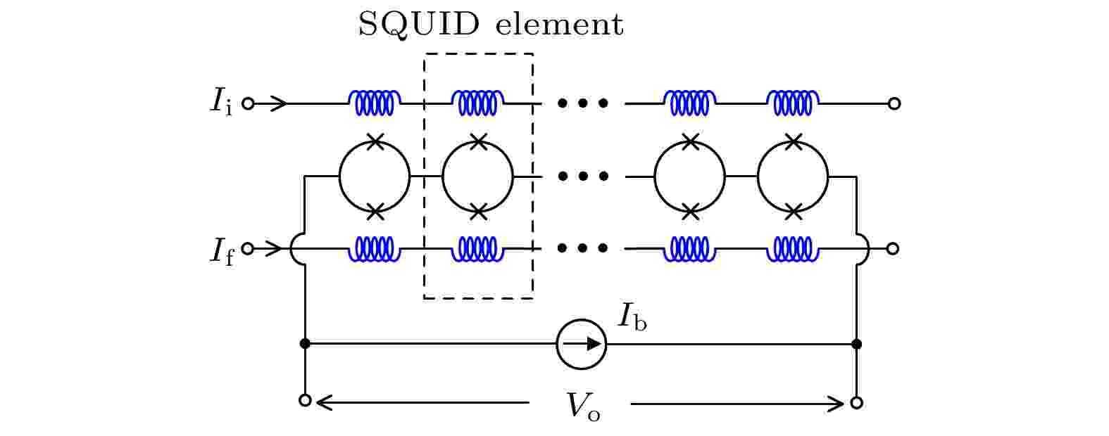
Superconducting quantum interference device (SQUID) has been used as an extremely sensitive flux sensor up to now. Series SQUID array (SSA) is made up of several identical element-SQUIDs in series, in which each element-SQUID is coupled with the same set of input coils by mutual inductance to realize the amplified output of the input current. From the noise viewpoint, each element-SQUID in SSA is independent of each other, resulting in the total voltage noise across the array rising linearly with the square root of the number of element-SQUIDs. From the perspective of input signals, since the signals come from the same set of input coils, the voltage output of the array is enlarged with the proportion of element-SQUID number, N. Taken together, the signal-to-noise ratio of SSA is increased by $\sqrt{ {N}}$ times, or the flux noise of SSA is reduced by 1/$\sqrt{ {N}}$ times compared with that of an element-SQUID ideally. However, with the increase in the number of element-SQUIDs in series, the chip design of SSA becomes more complicated, which puts forward higher requirements for the consistency and stability of its fabrication process. Besides, there exists a certain flux coherence between element-SQUIDs in SSA, whose normal operation depends on the working state of each element-SQUID in the array. In this paper, the fabrication of series SQUID array is carried on the autonomous superconducting micro-nano process platform, with a yield rate reaching over 80% on a 4-inch standard silicon wafer. Two kinds of SSAs with 200 and 800 element-SQUIDs, respectively, are integrated in a meandering way on a chip in a millimeter area. Home-made directly-coupled readout circuit is used to obtain the characteristics of SSA. The experimental results reveal that the flux noise at best working point is as low as 0.5μ$\varPhi _{\text{0}}/\sqrt{\text{Hz}}$ and the current sensitivity is about 35 μA/Φ0, thus, the equivalent input current noise is achieved at a level of 18 pA/$ \sqrt{\text{Hz}} $ . Additionally, the dependence of relevant parameters in array on the number of element-SQUIDs is verified, which is consistent with theoretical expectation basically. These show that the reliability of device design and the consistency of fabrication process perform well, thus laying the technical foundation for developing the low-noise SQUID amplifier and the multiplexed readout of low-impedance detectors.


2021, 70 (17): 178502.
doi: 10.7498/aps.70.20210325
Abstract +
As a type of two-dimensional (2D) semiconductor material, 2D germanium selenide (GeSe) exhibits excellent optoelectronic properties, and has potential applications in optoelectronic devices. The GeSe is a layered material with weak van der Waals interaction. Because of the high brittleness of GeSe, it is not easy to obtain 2D GeSe samples only by mechanical peeling technique. In order to obtain a thinner GeSe sheet, we use heat treatment to thin the bulk GeSe at a high temperature in vacuum. The GeSe samples obtained by mechanical peeling are placed in a tubular furnace with a pressure of 5 × 10⁻⁴ Pa for high temperature heating and thinning. In order to explore the better thinning effect, we set four temperatures to be at 320, 330, 340 and 350 ℃, respectively. After high temperature thinning, the samples are characterized and observed by atomic force microscope (AFM), scanning electron microscope (SEM), Raman spectrometer and photoluminescence (PL) spectrometer. From the above experiments, the GeSe nanosheet with a thickness of about 5 nm is prepared by mechanical peeling and high temperature thinning technology. Then, the electrical conductivities of GeSe nanosheets in oxygen (O2) and butane (C4H10) with different concentrations are evaluated by our designed experimental device. The results show that with the increase of oxygen concentration, the electrical conductivity of GeSe nanosheets increases. When the GeSe nanosheet is in butane gas, its conductivity under the same voltage decreases with the increase of the concentration of butane gas. In order to further analyze the mechanism of gas adsorption on GeSe nanosheets, we carry out the first-principles calculations. Our calculation results show that the adsorption energy of GeSe nanosheets for oxygen and butane is –4.555 eV and –4.865 eV, respectively. It is shown that both adsorption systems have a certain stability. The adsorption energy of C4H10 is smaller than that of O2, which corresponds to the smaller layer spacing of C4H10 than that of O2 on GeSe surface. From Bader analysis, it is shown that 0.262e is transferred from the surface of GeSe nanosheet to O2 molecule, which is much larger than 0.022e transferred from GeSe to C4H10 molecule. It can be inferred that the bond formed between GeSe and O2 molecule is covalent bond, while GeSe adsorption C4H10 is very fragile hydrogen bond adsorption. In an ideal condition (single atomic GeSe layer, no Se vacancy, and the device preparation process is vacuum), our calculation results show that C4H10 still has a weak ability to obtain electrons from the GeSe nanosheet. However, the complex conditions such as the actual layer thickness, the appearance of Se vacancy and the adsorption of O2 molecules on the surface leads to the difference between the experimental results and the theoretical calculations, which can be attributed to the adsorption of O2 molecules on the GeSe surface from the air during the processing of GeSe thinning and device fabrication. Owing to the high density of Se vacancies in the thin film, the high density of O2 adsorption is caused. Thus, butane gas is easy to lose electrons on the GeSe surface due to the O2 adsorption. In other words, electrons are transferred from butane gas molecules to the surface of GeSe film and neutralized with holes, which reduces the concentration of carriers and the concentration of holes in GeSe film, thus reducing the conductivity. Our research will contribute to the application of GeSe nanosheets in optoelectronic devices at the atmosphere of oxygen and butane.


2021, 70 (17): 178503.
doi: 10.7498/aps.70.20210434
Abstract +
β-Ga2O3-based deep-ultraviolet photodetector (PD) has versatile civil and military applications especially due to its inherent solar-blindness. In this work, pristine and N-doped β-Ga2O3 thin films are prepared on c-plane sapphire substrates by radio frequency magnetron sputtering. The influences of N impurity on the micromorphology, structural and optical properties of β-Ga2O3 film are investigated in detail by scanning electron microscopy, X-ray diffraction, and Raman spectra. The introduction of N impurities not only degrades the crystal quality of β-Ga2O3 films, but also affects the surface roughness. The β-Ga2O3 films doped with N undergoes a transition from a direct optical band gap to an indirect optical band gap. Then, the resulting metal-semiconductor-metal (MSM) PD is constructed. Comparing with the pure β-Ga2O3-based photodetector, the introduction of N impurities can effectively depress dark current and improve response speed of the β-Ga2O3 device. The N-doped β-Ga2O3-based photodetector achieves a dark current of 1.08 × 10⁻¹¹ A and a fast response speed (rise time of 40 ms and decay time of 8 ms), which can be attributed to the decrease of oxygen vacancy related defects. This study demonstrates that the acceptor doping provides a new opportunity for producing ultraviolet photodetectors with fast response for further practical applications.

2021, 70 (17): 178504.
doi: 10.7498/aps.70.20210274
Abstract +
The neural network under the current computer architecture is difficult to process complex data efficiently, thus becoming one of the bottlenecks restricting the development of artificial intelligence technology. The human brain has the characteristics of high efficiency, low power consumption and integration of memory and computing, and is regarded as a most potential computing system to break the traditional von Neumann computing system. Synaptic biomimetic device is to realize the neural mimicry of human brain from the hardware level. It can simulate the information processing mode of brain nerve, that is, the process of “memory” and “calculation” can be realized on the same device, which is of great significance in building a new computing system. In recent years, the fabrication of memristor materials for bio-mimetic synaptic devices has made progress, but most of them focus on the simulation of synaptic function. The key research of pulse signal perception and information transmission is relatively lacking. In this paper, an bi-layer memristor with structure Al/nc-Al AlN/A2O3/Ag is fabricated by rf sputtering method to realize the basic functions of bionic synaptic devices. It is found that this bio-mimetic memristor exhibits bipolar switching property which is the basic condition to produce memristor based neural synapse. Both of PPF and PPD process can be observed and there will be no firing signal observed if the pulse interval is as large as 350 ms. The change of device conductance should be related to pulse voltage, frequency and pulse number applied. The larger pulse voltage, frequency and number will cause device conductance to increase sharply in both positive and negative pulse voltage region. The STDP measurement is executed with different sequence pulses from post and previous neuron separately. If the pulse of previous synapse comes in front of pulse from post synapse, the conductance will increase, which is so-called LTP process. If the pulse of previous neuron comes behind of pulse from post neuron, the conductance will be reduced as well. Triplet STDP measurement is executed with at least three pulses from previous and post neuron at the meanwhile. It is concluded that if the interval time of the first two pulses is fixed, the device conductance more depends on the value of the second and third pulse interval. Ebbinghaus forgetting curve can be used to explain the reason why the device conductance declines with time going by. The stability study of this memristor includes endurance and retention properties at both room and high temperature. It is found this biomimetic memristor can maintain its conductance for over 115.7 days at 85 ℃, which is long enough for current neural network design.
2021, 70 (17): 178505.
doi: 10.7498/aps.70.20210116
Abstract +
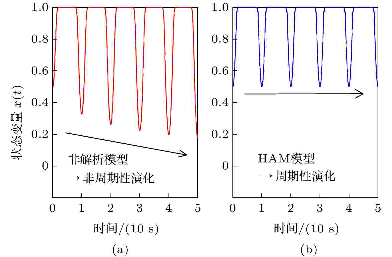
Memristive networks are large-scale non-linear circuits based on memristor cells, playing a crucial role in developing the emerging researches such as next-generation artificial intelligence, bioelectronics, and high-performance memory. The performance of memristive networks is greatly affected by the memristor model describing physical and electrical characteristics of a memristor cell. However, existing models are mainly non-analytic and, accordingly, may have convergence issues in their applications in memristive networks’ analyses. Therefore, aiming at improving convergence of memristive networks, we propose an analytic modeling strategy for memristor based on homotopy analysis method (HAM). In this strategy, the HAM is used to obtain an analytic memristor model through solving the state equations of memristors in original physical model. Specifically, the HAM is used to solve the analytic approximate solution of the core parameter of memristor—state variable, from the state equations, in the form of analytic homotopy series. Then the analytic approximate model of memristor is obtained by using the solved state variables. The characteristics of the proposed strategy are as follows. 1) Its solution has a closed-form expression, i.e. an explicit function, 2) its approximation error is optimized, thereby realizing the convergence optimization. Moreover, according to the characteristics of memristive networks, we introduce an analysis criterion for memristor model applicable to memristive networks. Through the long-time evolution experiments of a memristor cell and a benchmark memristive matrix network with different inputs, and the comparisons with the traditional non-analytic (numeric) method, we verify the analyticity and convergence superiority of the modeling strategy. Besides, based on this strategy and the comparison experiments, we reveal that one of the underlying reasons for non-convergence in the large-scale memristive network simulation possesses the non-analyticity of the used memristor model. The strategy can be further used for analyzing the performances of a memristor cell and memristive networks in long-time. It also has potential applications in emerging technologies.
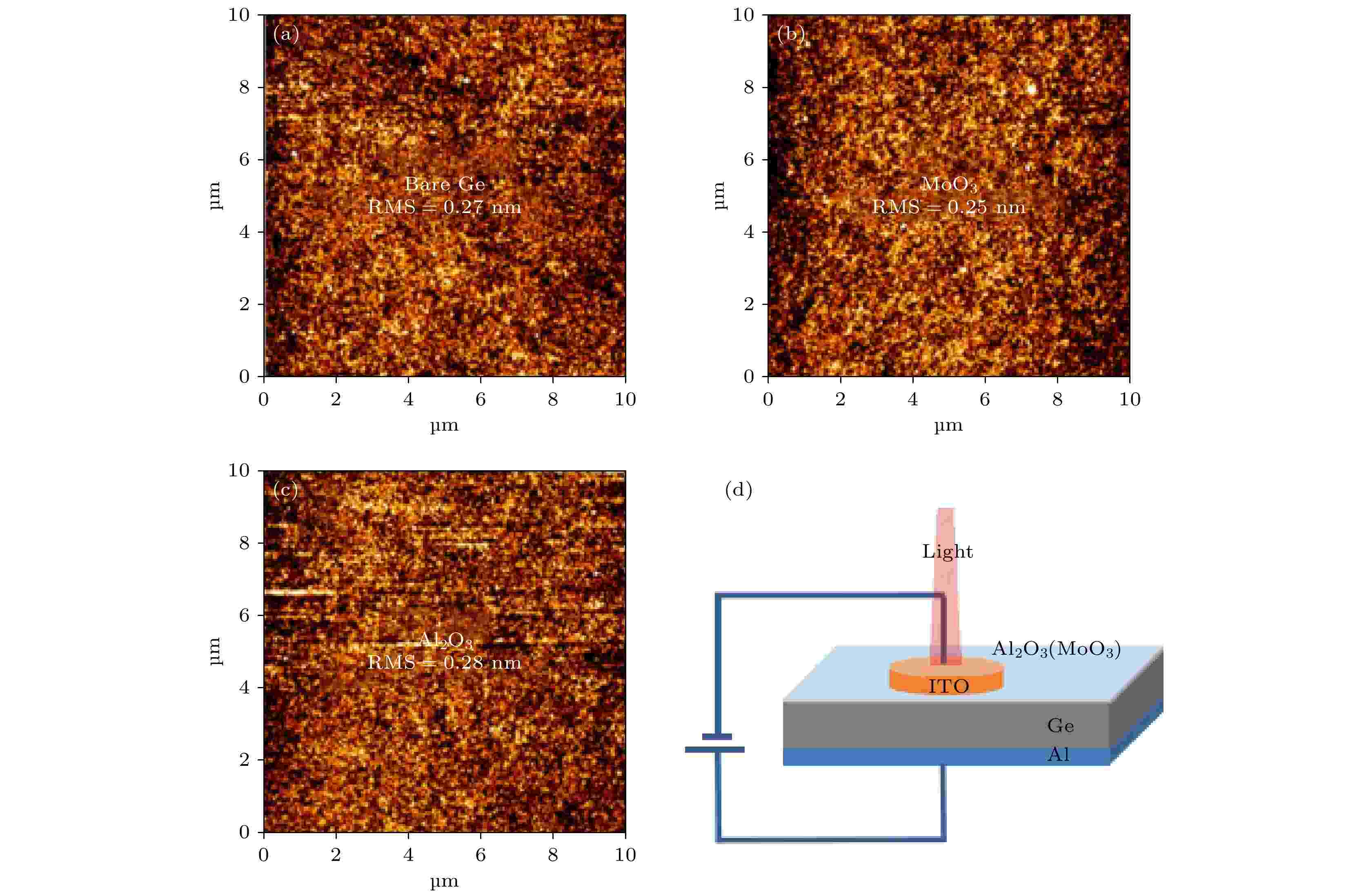
2021, 70 (17): 178506.
doi: 10.7498/aps.70.20210138
Abstract +
Germanium (Ge) photodetectorhas been considered as one of the promising optoelectronic devices for optoelectronic integration. So far, most of reported Ge photodetectors with bulk Ge show high dark currents and low responsivities. In this paper, ultra-thin dielectric interlayer-modulated indium tin oxid (ITO)/Ge Schottky photodetectors with high responsivities and low dark currents are investigated, in which the ultra-thin dielectric interlayers are deposited through atomic layer deposition. The characteristics of ITO/Al2O3 (or MoO3)/Ge Schottky photodiodes fabricated on bulk Ge wafers with various doping concentrations and Ge epilayer on silicon substrates are comparatively studied. It is found that the 2-nm-thick Al2O3 intercalation between ITO transparent electrode and Ge can effectively enhance the Schottky barrier heights of the photodetectors and trap holes at interface states, rendering their dark currents low and responsivities high. The effective Schottky barrier heights increase from 0.34 eV (ITO/i-Ge) to 0.55 eV (ITO/Al2O3/i-Ge), and from 0.24 eV (ITO/n-Ge) to 0.56 eV (ITO/Al2O3/n-Ge). While MoO3 intercalation between ITO and Ge has no significant effect on the characteristics of all of the photodetectors due to its large electron affinity. The best performance is realized on the ITO/Al2O3/i-Ge photodetector with a low dark current of 5.91 mA/cm–2 at –4 V, sharply dropping by two orders of magnitude, compared with that of the ITO/i-Ge photodetector without the Al2O3 interlayer, and the responsivity is significantly improved to 4.11 A/W at 1310 nm. The ITO/Al2O3/epi-Ge photodetector fabricated on 500 nm Ge epilayer on a silicon substrate also shows the improved performance with a dark current density of 226.70 mA/cm2 at –3 V and a responsivity of 0.38 A/W at 1310 nm, compared with ITO/epi-Ge photodetector. Finally, experiment studies of single-point infrared images at 1310 nm and 1550 nm are carried out with the ITO/Al2O3/i-Ge photodetector on a two-dimensional XY displacement platform, which contains 25 pixels and a total detection size of 1750 μm × 1750 μm. The clear and distinguishable images of the infrared spot position are obtained. Consequently, these results suggest that the dielectric interlayer- modulated Schottky photodetectors are competitive in low power consumption and high responsivity, and have great potential applications in the civil field of short wave infrared imaging.

EDITOR'S SUGGESTION
2021, 70 (17): 178701.
doi: 10.7498/aps.70.20210477
Abstract +
In recent years, the emergence and development of single-molecule tracking technology has provided a new way to study the biological process in a cell membrane. However, the heterogeneity of biomolecular motions in cell membranes makes it difficult to distinguish and separate different molecular motion patterns from a large number of molecular trajectories. In this work, taking the system of interaction between melittin and a single-component supported phospholipid bilayer (SLB) membrane as an example, a type of data analysis method is developed through using the frequency distribution of standard deviations of single molecular motion displacements to distinguish and separate lipid molecules in different motion modes. It provides higher accuracy and more quantitative information than traditional analysis methods based on the frequency distribution of displacement or radius of gyration. By using this method, we successfully separate the two moving states of lipids in the SLB, and find that such a distribution is partly consistent with the location distribution of lipids in the upper leaflet and lower leaflet. Under the influence of surface adsorption or transmembrane poration of melittin at different concentrations, the movements of these two types of lipids are disturbed in different ways. In this work, a data analysis method for the separation of molecular motion patterns is developed according to the complex heterogeneity of molecular motions in a phospholipid membrane system. The different effects on the upper leaflet and lower leaflet of a lipid membrane due to melittin actions at different stages are obtained. The method developed in this work will be of great help in studying the dynamic processes of biological systems by using single-molecule tracking technology.
2021, 70 (17): 178901.
doi: 10.7498/aps.70.20210453
Abstract +
For many real world systems ranging from biology to engineering, efficient network computation methods have attracted much attention in many applications. Generally, the performance of a network computation can be improved in two ways, i.e., rewiring and weighting. As a matter of fact, many real-world networks where an interpretation of efficient computation is relevant are weighted and directed. Thus, one can argue that nature might have assigned the optimal structure and weights to adjust the level of functionality. Indeed, in many neural and biochemical networks there is evidence that the synchronized and coordinated behavior may play important roles in the system’s functionality. The importance of the network weighting is not limited to the nature. In computer networks, for example, designing appropriate weights and directions for the connection links may enhance the ability of the network to synchronize the processes, thus leading the performance of computation to improve. In this paper, we propose a new two-mode weighting strategy by employing the network topological centralities including the degree, betweenness, closeness and communication neighbor graph. The weighting strategy consists of two modes, i.e., the original mode, in which the synchronizability is enhanced by increasing the weight of bridge edges, and the inverse version, in which the performance of community detection is improved by reducing the weight of bridge edges. We control the weight strategy by simply tuning a single parameter, which can be easily performed in the real world systems. We test the effectiveness of our model in a number of artificial benchmark networks as well as real-world networks. To the best of our knowledge, the proposed weighting strategy outperforms previously published weighting methods of improving the performance of network computation.
GEOPHYSICS, ASTRONOMY, AND ASTROPHYSICS

EDITOR'S SUGGESTION
2021, 70 (17): 179501.
doi: 10.7498/aps.70.20210603
Abstract +
Aiming at improving the beam quality of thin-wall tube laser, a novel method based on the right-angle cone deformable mirror is proposed. In the method, a reflector with inner right-angle conical surface is used, and the annular laser beam successively passes through the opposite sides of the tube, compensating for the off-axis aberrations of the annular laser beam. Next, the residual aberrations are corrected by the deformation of the right-angle cone mirror to further improve the beam quality. The physical model of the right-angle cone deformable mirror is built up by using the finite element analysis method, followed by optimizing the structural parameters of the right-angle cone deformable mirror. The preliminarily optimized right-angle cone deformable mirror drived by 48 actuators with a radius of 1.5 mm for each actuator and an interval of 11 mm between actuators is then utilized to correct the beam quality of the thin-wall tube laser. Results indicate that the output beam quality of the thin-wall tube laser degrades rapidly with the increasing of the tube’s concentricity error, parallelism error, taper error and source’s parallelism error. Fortunately, the beam quality is significantly improved by using the right-angle cone deformable mirror and the β factor greatly decreases. In addition, the performance of the non-ideal right-angle cone deformable mirror with a 20-μrad taper error and a 10-mrad collimation error is compared with that of the ideal mirror, and the results show that the β factor is controlled within 1.14 after having been corrected by the non-ideal right-angle cone deformable mirror. Therefore, the simulation results theoretically prove that the novel method can effectively eliminate the typical aberrations caused by the errors from fabrication and alignment and correct the wavefront distortion of the large-aperture thin-wall tube laser, thus significantly improving the beam quality.
