


-
Two-dimensional (2D) materials exhibit massive potential in research and development in the scientific world due to their unique electrical, optical, thermal and mechanical properties. Graphene is an earliest found two-dimensional material, which has many excellent properties, such as high carrier mobility and large surface area. However, single layer graphene has a zero band gap, which limits its response in electronic devices. Unlike graphene, the transition metal sulfides (TMDs) have various band structures and chemical compositions, which greatly compensate for the defect of zero gap in graphene. The WS2 is one of the 2D TMDs exhibiting a series of unique properties, such as strong spin-orbit coupling, band splitting and high nonlinear susceptibility, which make it possess many applications in semiconducting optoelectronics and micro/nano-electronics. The 2D semiconductors along with semimetallic graphene are seen as basic building blocks for a new generation of nanoelectronic devices. In this way, the artificially designed TMD heterostructure is a promising option for ultrathin photodetectors. There are few reports on the physical mechanism of carrier mobility and charge distribution at the interface of WS2/graphene heterostructure, by varying the interfacial distance of WS2/graphene heterostructure to investigate the effect on the electronic properties. Here in this work, the corresponding effects of interface cohesive interaction and electronic properties of WS2/graphene heterostructure are studied by first-principles method. The calculation results indicate that the lattice mismatch between monolayer WS2 and graphene is low, the equilibrium layer distance d of about 3.42 Å for the WS2/graphene heterostructure and a weak van der Waals interaction forms in interface. Further, by analyzing the energy band structures and the three-dimensional charge density difference of WS2/graphene, we can identify that at the interface of the WS2 layer there appears an obvious electron accumulation: positive charges are accumulated near to the graphene layer, showing that WS2 is an n-type semiconductor due to the combination with graphene. Furthermore, the total density of states and corresponding partial density of states of WS2/graphene heterostructure are investigated, and the results show that the valence band is composed of hybrid orbitals of W 5d and C 2p, whereas the conduction band is comprised of W 5d and S 3p orbitals, the orbital hybridization between W 5d and S 3p will cause photogenerated electrons to transfer easily from the internal W atoms to the external S atoms, thereby forming a build-in internal electric field from graphene to WS2. Finally, by varying the interfacial distance for analyzing the Schottky barrier transition, as the interfacial distance is changed greatly from 2.4 Å to 4.2 Å, the shape of the band changes slightly, however, the Fermi level descends relatively gradually, which can achieve the transition from a p-type Schottky contact to an n-type Schottky contact in the WS2/graphene. The plane-averaged charge density difference proves that the interfacial charge transfer and the Fermi level shift are the reasons for determining the Schottky barrier transition in the WS2/graphene heterostructure. Our studies may prove to be instrumental in the future design and fabrication of van der Waals based field effect transistors.
-
Keywords:
- heterostructure /
- band structure /
- Schottky contact /
- first-principles
[1] Cao M S, Shu J C, Wang X X, Wang X, Zhang M, Yang H J, Fang X Y, Yuan J 2019 Ann. Phys. (Berlin)
2019 1800390  Google Scholar
[2] Wen B, Cao M S, Lu M M , Cao W Q, Shi H L, Liu J, Wang X X, Jin H B , Fang X Y, Wang W Z , Yuan J 2014 Adv. Mater. 26 3484
Google Scholar
[3] Cao M S, Wang X X, Cao W Q, Fang X Y, Wen B, Yuan J 2018 Small 14 1800987
Google Scholar
[4] Cao M S, Song W L, Hou Z L, Wen B, Yuan J 2010 Carbon 48 788
Google Scholar
[5] Liu Z F, Liu Q, Huang Y, Ma Y F, Yin S G, Zhang X Y, Sun W, Chen Y S 2008 Adv. Mater. 20 3924
Google Scholar
[6] Castro N A H, Guinea F, Peres N M R, Novoselov K S, Geim A K 2009 Rev. Mod. Phys. 81 109
Google Scholar
[7] Ferrari A C, Meyer J C, Scardaci V, Casiraghi C, Lazzeri M, Mauri F, Piscanec S, Jiang D, Novoselov K S, Roth S, Geim A K 2006 Phys. Rev. Lett. 97 187401
Google Scholar
[8] Zhao H, Guo Q S, Xia F N, Wang H 2015 Nanophotonics 4 128
Google Scholar
[9] Yang L Y, Sinitsyn N A, Chen W B, Yuan J T, Zhang J, Lou J, Crooker S A 2015 Nat. Phys. 11 830
Google Scholar
[10] Zeng H L, Liu G B, Dai J F, Yan Y J, Zhu B R, He R C, Xie L S, Xu J, Chen X H, Yao W, Cui X D 2013 Sci. Rep. 3 1608
Google Scholar
[11] Britnell L, Ribeiro R M, Eckmann A, Jalil R, Belle B D, Mishchenko A Y J, Gorbachev R V, Georgiou T, Morozov S V, Grigorenko A N, Geim A K, Casiraghi C, Neto A H C, Novoselov K S 2013 Science 340 1311
Google Scholar
[12] Georgiou T, Yang H F, Jalil R, Chapman J, Novoselov K S, Mishchenko A 2014 Dalton Trans. 43 10388
Google Scholar
[13] Chen K T, Chang S T H 2017 Vacuum 140 172
Google Scholar
[14] Cong C X, Shang J Z, Wang Y L, Yu T 2018 Adv. Opt. Mater. 6 1700767
Google Scholar
[15] Iqbal M W, Iqbal M Z, Khan M F 2016 RSC Adv. 6 24675
Google Scholar
[16] Yue Y, Chen J, Zhang Y, Ding S, Zhao F, Wang Y, Feng W 2018 ACS Appl. Mater. Interfaces DOI: 10.1021/acsami. 8b05885
[17] Hong X, Kim J, Shi S F, Zhang Y, Jin C, Sun Y, Tongay S, Wu J, Zhang Y, Wang F 2014 Nat. Nanotechnol. 9 682
Google Scholar
[18] Ma Y D, Dai Y, Guo M, Niu C W, Huang B B 2011 Nanoscale 3 3883
Google Scholar
[19] Li X D, Yu S, Wu S Q, Wen Y H, Zhou S, Zhu Z Z 2013 J. Phys. Chem. C 117 15347
Google Scholar
[20] Dean C R, Young A F, Meric I, Lee C, Wang L, Sorgenfrei S, Watanabe K, Taniguchi T, Kim P, Shepard K L, Hone J 2010 Nat. Nanotechnol. 5 722
Google Scholar
[21] Lin X, Xu Y, Hakro A A, Hasan T, Hao R, Zhang B L, Chen H S 2013 J. Mater. Chem. C 1 1618
Google Scholar
[22] Xue J M, Sanchez-Yamagishi J, Bulmash D, Jacquod P, Deshpande A, Watanabe K, Taniguchi T, Jarillo Herrero P, Leroy B J 2011 Nat. Mater. 10 282
Google Scholar
[23] Neek A M, Sadeghi A, Berdiyorov G R, Peeters F M 2013 Appl. Phys. Lett. 103 261904
Google Scholar
[24] Cai Y, Chu C P, Wei C M, Chou M Y 2013 Matter Mater. Phys. 88 245408
Google Scholar
[25] Zhang F, Li W, Ma Y Q, Tang Y N, Dai X Q 2017 RSC Adv. 7 29350
Google Scholar
[26] Tan H J, Xu W S, Sheng Y W, Lau C S, Fan Y, Chen Q, Wang X C, Zhou Y Q, Warner J H 2017 Adv. Mater. 29 1702917
Google Scholar
[27] 危阳, 马新国, 祝林, 贺华, 黄楚云 2017 物理学报 66 087101
Google Scholar
Wei Y, Ma X G, Zhu L, He H, Huang C Y 2017 Acta Phys. Sin. 66 087101
Google Scholar
[28] Jin C J, Rasmussen F A, Thygesen K S 2015 J. Phys. Chem. C 119 19928
Google Scholar
[29] Liu B, Wu L J, Zhao Y Q, Wang L Z, Cai M Q 2016 RSC Adv. 6 60271
Google Scholar
[30] Jiang J W 2015 Front. Phys. 10 287
Google Scholar
[31] Segall M D, Lindan P J D, Probert M J, Pickard C J, Hasnip P J, Clark S J, Payne M C 2002 J. Phys.: Condens. Matter. 14 2717
Google Scholar
[32] Vanderbilt D 1990 Phys. Rev. B 41 7892
Google Scholar
[33] Tkatchenko A, Scheffler M 2009 Phys. Rev. Lett. 102 073005
Google Scholar
[34] Monkhorst H J, Pack J D 1976 Phys. Rev. B 13 5188
Google Scholar
[35] Ma X G, Hu J S, He H, Dong S J, Huang C Y, Chen X B 2018 ACS Appl. Nano Mater. 1 5507
Google Scholar
[36] Björkman T, Gulans A, Krasheninnikov A V, Nieminen R M 2012 Phys. Rev. Lett. 108 235502
Google Scholar
[37] Hu J S, Ji G P, Ma X G, He H, Huang C Y 2018 Appl. Surf. Sci. 440 35
Google Scholar
[38] Ding Y, Wang Y L, Ni J, Shi L, Shi S Q, Tang W H 2011 Physica B 406 2254
Google Scholar
[39] Du A J, Sanvito S, Li Z, Wang D W, Jiao Y, Liao T, Sun Q, Ng Y H, Zhu Z H, Amal R, Smith S C 2012 J. Am. Chem. Soc. 134 4393
Google Scholar
[40] Zhou W, Zou X L, Najmaei S 2013 Nano Lett. 13 2615
Google Scholar
[41] Li X E, Basile L, Huang B 2015 ACS Nano 9 8078
Google Scholar
[42] Wang Q H, Kalantar-Zadeh K, Kis A 2012 Nature Nanotechnol. 7 699
Google Scholar
[43] Zhang Y W, Li H, Wang L, Xie X M, Zhang S L, Liu R, Qiu Z J 2015 Sci. Reports 5 7938
Google Scholar
[44] Fang X Y, Yu X X, Zheng H M, Jin B, Wang L, Cao M S 2015 Phys. Lett. A 379 2245
Google Scholar
-

图 1 单层二硫化钨/石墨烯异质结匹配模型的顶视图 (a)单层二硫化钨3 × 3 × 1超胞与石墨烯4 × 4 × 1超胞的匹配模型; (b)单层二硫化钨4 × 4 × 1超胞与石墨烯5 × 5 × 1超胞的匹配模型
Figure 1. Top views of two match configurations of monolayer WS2/graphene heterostructure: (a) Match configuration between 3 × 3 × 1 lateral periodicity of monolayer WS2 sheet and 4 × 4 × 1 lateral periodicity of graphene; (b) match configuration between 4 × 4 × 1 lateral periodicity of monolayer WS2 sheet and 5 × 5 × 1 lateral periodicity of graphene.
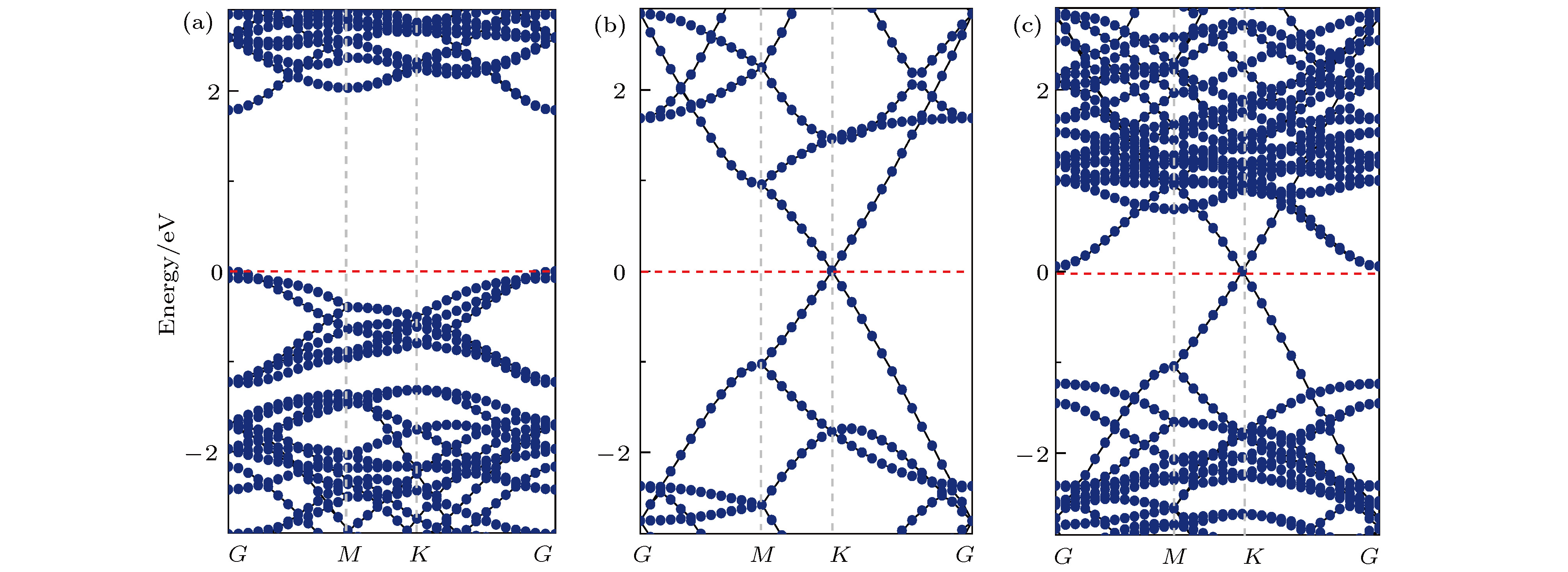
图 2 单层二硫化钨(a)、石墨烯(b)和二硫化钨/石墨烯异质结(c)的能带结构, 其中费米能级处在0 eV, 用红色的虚线表示
Figure 2. Energy band structures of (a) WS2 monolayer, (b) graphene and (c) WS2/graphene heterostructure. The Fermi levels are set to zero and marked by red dashed lines.
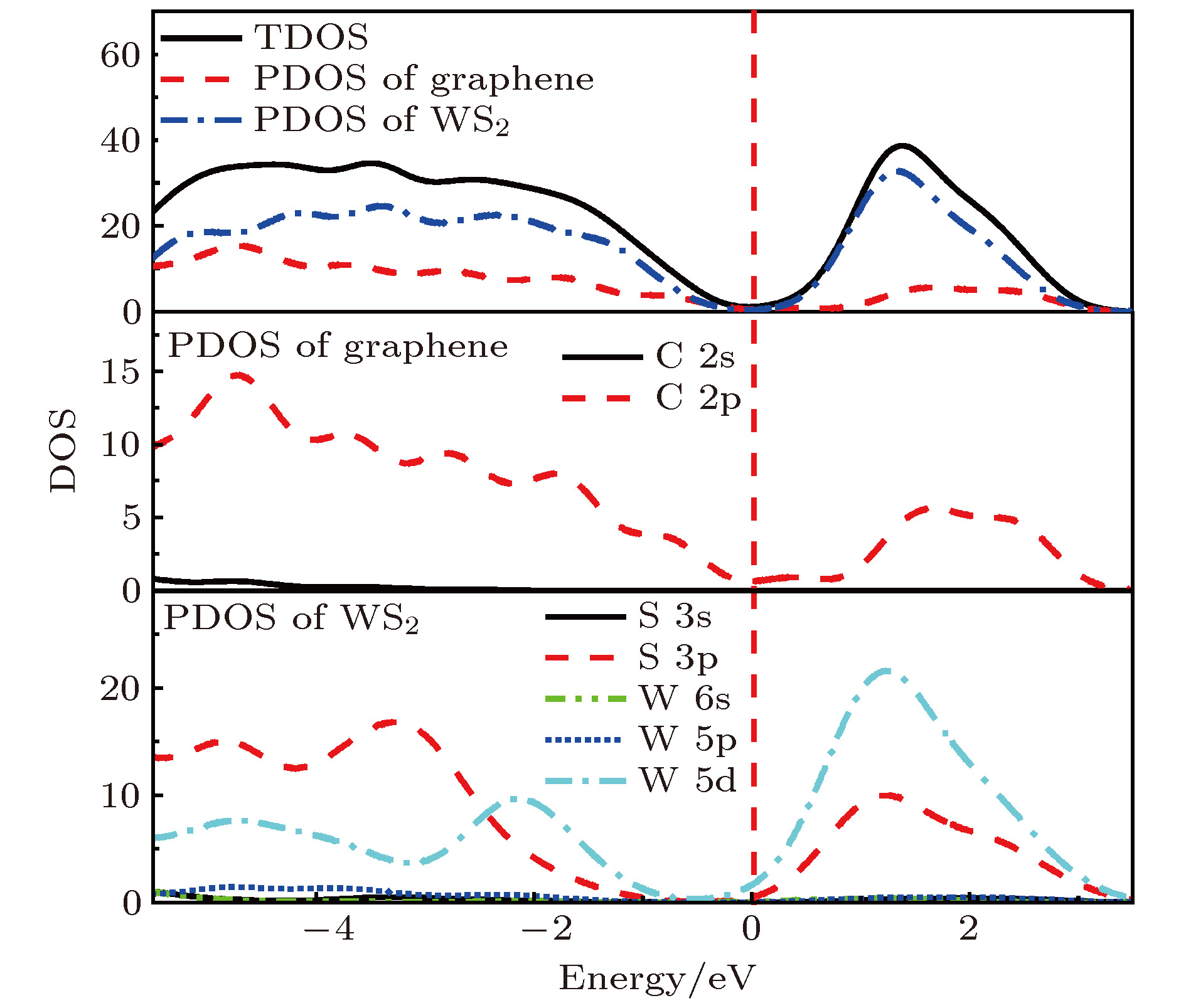
图 3 二硫化钨/石墨烯异质结的总态密度以及相应的分态密度
Figure 3. Calculated total density of states (TDOS) and the corresponding partial density of states (PDOS) of WS2/graphene heterostructure.
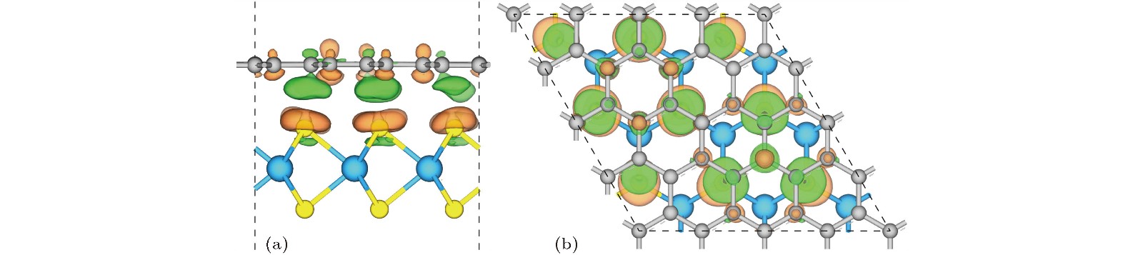
图 4 二硫化钨/石墨烯异质结的三维电子密度差分图 (a)侧视图; (b)顶视图
Figure 4. Three-dimensional charge density difference plots WS2/graphene heterostructure: (a) Side view; (b) top view.
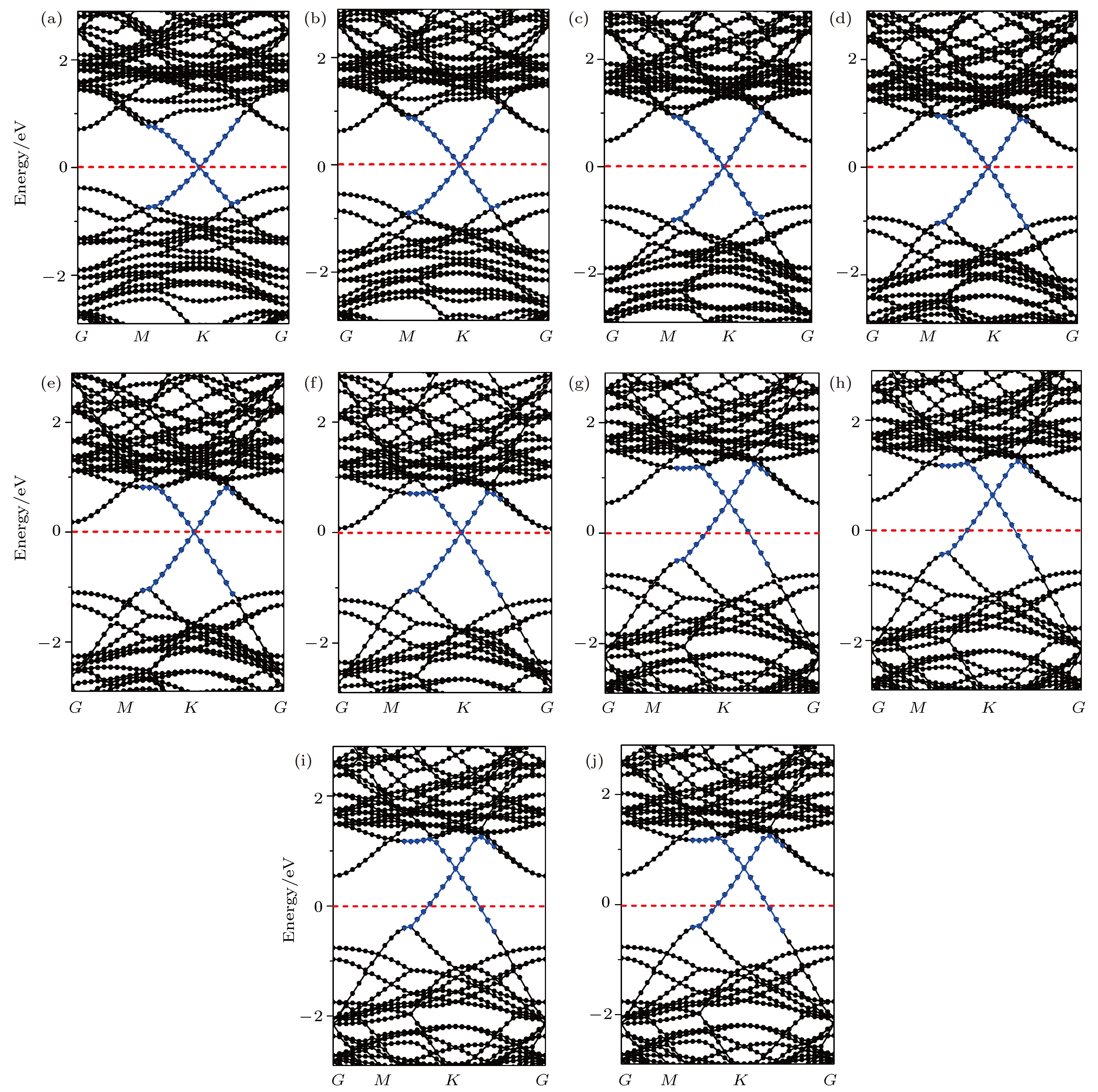
图 5 不同层间距下的二硫化钨/石墨烯异质结的能带图, 其中蓝色曲线代表石墨烯部分的贡献 (a)−(j)分别代表层间距为2.4, 2.6, 2.8, 3.0, 3.2, 3.4, 3.6, 3.8, 4.0, 4.2 Å, 费米能级处在0 eV, 用红色虚线表示
Figure 5. Band structures of WS2/graphene heterostructure under different interface distances. Blue curves denote the contributions from graphene. Panels (a)−(j) correspond to the interface distances of 2.4, 2.6, 2.8, 3.0, 3.2, 3.4, 3.6, 3.8, 4.0, 4.2 Å, respectively. The Fermi level is set to zero and marked by red dotted line.
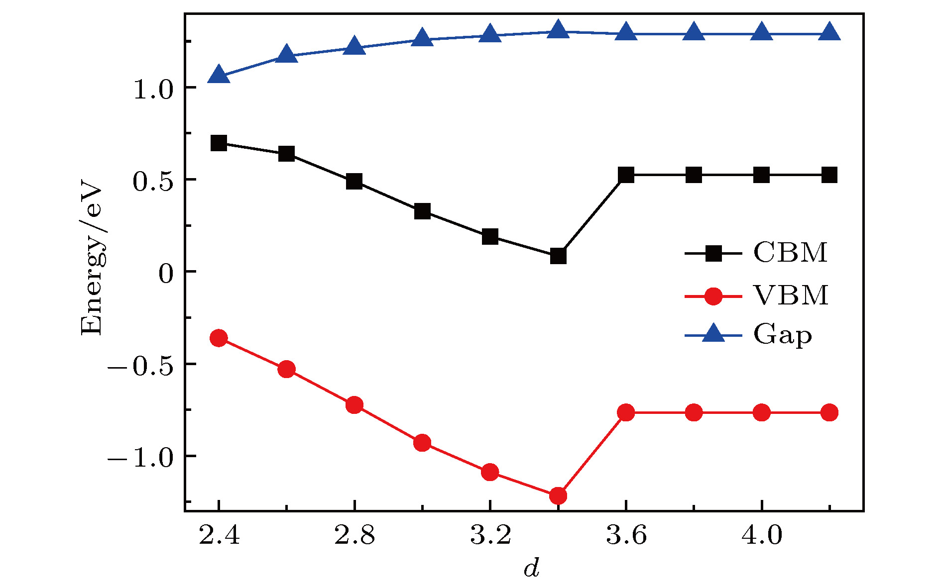
图 6 二硫化钨/石墨烯异质结中二硫化钨部分的导带底、价带顶和带隙在不同层间距的值
Figure 6. Conduction band minimum (CBM), valence band maximum (VBM) and band gap of WS2 monolayer in the WS2/graphene heterostructure as a function of interfacial distance.

图 7 不同层间距下二硫化钨/石墨烯异质结沿着Z方向的平面差分电荷密度图
Figure 7. Plots of the plane-averaged electron density difference along the direction perpendicular to the interface of the WS2/graphene heterostructure under different interface distances of 2.4 Å to 4.2 Å, respectively.
-
[1] Cao M S, Shu J C, Wang X X, Wang X, Zhang M, Yang H J, Fang X Y, Yuan J 2019 Ann. Phys. (Berlin)
2019 1800390 Google Scholar
[2] Wen B, Cao M S, Lu M M , Cao W Q, Shi H L, Liu J, Wang X X, Jin H B , Fang X Y, Wang W Z , Yuan J 2014 Adv. Mater. 26 3484
Google Scholar
[3] Cao M S, Wang X X, Cao W Q, Fang X Y, Wen B, Yuan J 2018 Small 14 1800987
Google Scholar
[4] Cao M S, Song W L, Hou Z L, Wen B, Yuan J 2010 Carbon 48 788
Google Scholar
[5] Liu Z F, Liu Q, Huang Y, Ma Y F, Yin S G, Zhang X Y, Sun W, Chen Y S 2008 Adv. Mater. 20 3924
Google Scholar
[6] Castro N A H, Guinea F, Peres N M R, Novoselov K S, Geim A K 2009 Rev. Mod. Phys. 81 109
Google Scholar
[7] Ferrari A C, Meyer J C, Scardaci V, Casiraghi C, Lazzeri M, Mauri F, Piscanec S, Jiang D, Novoselov K S, Roth S, Geim A K 2006 Phys. Rev. Lett. 97 187401
Google Scholar
[8] Zhao H, Guo Q S, Xia F N, Wang H 2015 Nanophotonics 4 128
Google Scholar
[9] Yang L Y, Sinitsyn N A, Chen W B, Yuan J T, Zhang J, Lou J, Crooker S A 2015 Nat. Phys. 11 830
Google Scholar
[10] Zeng H L, Liu G B, Dai J F, Yan Y J, Zhu B R, He R C, Xie L S, Xu J, Chen X H, Yao W, Cui X D 2013 Sci. Rep. 3 1608
Google Scholar
[11] Britnell L, Ribeiro R M, Eckmann A, Jalil R, Belle B D, Mishchenko A Y J, Gorbachev R V, Georgiou T, Morozov S V, Grigorenko A N, Geim A K, Casiraghi C, Neto A H C, Novoselov K S 2013 Science 340 1311
Google Scholar
[12] Georgiou T, Yang H F, Jalil R, Chapman J, Novoselov K S, Mishchenko A 2014 Dalton Trans. 43 10388
Google Scholar
[13] Chen K T, Chang S T H 2017 Vacuum 140 172
Google Scholar
[14] Cong C X, Shang J Z, Wang Y L, Yu T 2018 Adv. Opt. Mater. 6 1700767
Google Scholar
[15] Iqbal M W, Iqbal M Z, Khan M F 2016 RSC Adv. 6 24675
Google Scholar
[16] Yue Y, Chen J, Zhang Y, Ding S, Zhao F, Wang Y, Feng W 2018 ACS Appl. Mater. Interfaces DOI: 10.1021/acsami. 8b05885
[17] Hong X, Kim J, Shi S F, Zhang Y, Jin C, Sun Y, Tongay S, Wu J, Zhang Y, Wang F 2014 Nat. Nanotechnol. 9 682
Google Scholar
[18] Ma Y D, Dai Y, Guo M, Niu C W, Huang B B 2011 Nanoscale 3 3883
Google Scholar
[19] Li X D, Yu S, Wu S Q, Wen Y H, Zhou S, Zhu Z Z 2013 J. Phys. Chem. C 117 15347
Google Scholar
[20] Dean C R, Young A F, Meric I, Lee C, Wang L, Sorgenfrei S, Watanabe K, Taniguchi T, Kim P, Shepard K L, Hone J 2010 Nat. Nanotechnol. 5 722
Google Scholar
[21] Lin X, Xu Y, Hakro A A, Hasan T, Hao R, Zhang B L, Chen H S 2013 J. Mater. Chem. C 1 1618
Google Scholar
[22] Xue J M, Sanchez-Yamagishi J, Bulmash D, Jacquod P, Deshpande A, Watanabe K, Taniguchi T, Jarillo Herrero P, Leroy B J 2011 Nat. Mater. 10 282
Google Scholar
[23] Neek A M, Sadeghi A, Berdiyorov G R, Peeters F M 2013 Appl. Phys. Lett. 103 261904
Google Scholar
[24] Cai Y, Chu C P, Wei C M, Chou M Y 2013 Matter Mater. Phys. 88 245408
Google Scholar
[25] Zhang F, Li W, Ma Y Q, Tang Y N, Dai X Q 2017 RSC Adv. 7 29350
Google Scholar
[26] Tan H J, Xu W S, Sheng Y W, Lau C S, Fan Y, Chen Q, Wang X C, Zhou Y Q, Warner J H 2017 Adv. Mater. 29 1702917
Google Scholar
[27] 危阳, 马新国, 祝林, 贺华, 黄楚云 2017 物理学报 66 087101
Google Scholar
Wei Y, Ma X G, Zhu L, He H, Huang C Y 2017 Acta Phys. Sin. 66 087101
Google Scholar
[28] Jin C J, Rasmussen F A, Thygesen K S 2015 J. Phys. Chem. C 119 19928
Google Scholar
[29] Liu B, Wu L J, Zhao Y Q, Wang L Z, Cai M Q 2016 RSC Adv. 6 60271
Google Scholar
[30] Jiang J W 2015 Front. Phys. 10 287
Google Scholar
[31] Segall M D, Lindan P J D, Probert M J, Pickard C J, Hasnip P J, Clark S J, Payne M C 2002 J. Phys.: Condens. Matter. 14 2717
Google Scholar
[32] Vanderbilt D 1990 Phys. Rev. B 41 7892
Google Scholar
[33] Tkatchenko A, Scheffler M 2009 Phys. Rev. Lett. 102 073005
Google Scholar
[34] Monkhorst H J, Pack J D 1976 Phys. Rev. B 13 5188
Google Scholar
[35] Ma X G, Hu J S, He H, Dong S J, Huang C Y, Chen X B 2018 ACS Appl. Nano Mater. 1 5507
Google Scholar
[36] Björkman T, Gulans A, Krasheninnikov A V, Nieminen R M 2012 Phys. Rev. Lett. 108 235502
Google Scholar
[37] Hu J S, Ji G P, Ma X G, He H, Huang C Y 2018 Appl. Surf. Sci. 440 35
Google Scholar
[38] Ding Y, Wang Y L, Ni J, Shi L, Shi S Q, Tang W H 2011 Physica B 406 2254
Google Scholar
[39] Du A J, Sanvito S, Li Z, Wang D W, Jiao Y, Liao T, Sun Q, Ng Y H, Zhu Z H, Amal R, Smith S C 2012 J. Am. Chem. Soc. 134 4393
Google Scholar
[40] Zhou W, Zou X L, Najmaei S 2013 Nano Lett. 13 2615
Google Scholar
[41] Li X E, Basile L, Huang B 2015 ACS Nano 9 8078
Google Scholar
[42] Wang Q H, Kalantar-Zadeh K, Kis A 2012 Nature Nanotechnol. 7 699
Google Scholar
[43] Zhang Y W, Li H, Wang L, Xie X M, Zhang S L, Liu R, Qiu Z J 2015 Sci. Reports 5 7938
Google Scholar
[44] Fang X Y, Yu X X, Zheng H M, Jin B, Wang L, Cao M S 2015 Phys. Lett. A 379 2245
Google Scholar

 DownLoad:
Catalog
Metrics
- Abstract views: 11765
- PDF Downloads: 324
- Cited By: 0
