


-
超导纳米线单光子探测器(SNSPD)优异的时间特性(时间抖动和响应速度)是其最具吸引力的优势之一, 并且已在量子通信、量子计算等领域中得到广泛应用. 然而, 由于SNSPD的各技术参数之间相互牵制, 使得进一步提升SNSPD综合性能存在技术挑战. 小光敏面SNSPD在时间特性上具有明显优势, 但同时存在探测效率低的突出问题. 本文为面向量子信息应用的光纤耦合探测器, 从开发实用化、产品化SNSPD出发, 采用批量对准、高效耦合的自对准封装结构, 围绕小光敏面自对准SNSPD综合性能的提升展开研究. 采用发散小、易刻蚀的Au/SiO2光学腔, 在提高纳米线光吸收效率的同时通过优化自对准芯片外轮廓加工精度的方式来提高自对准SNSPD的光耦合效率, 并完成了配套的工艺研发. 并通过小芯径光纤从器件封装角度提升耦合效率. 除此之外, 探测器的双层纳米线结构使其拥有更低的动态电感和更高的超导转变电流, 进一步优化了器件的时间特性. 实验制备的探测器在2.2 K温度下于1310 nm处达到最大效率82%, 并且在1200—1600 nm波长范围内均有65%以上的系统探测效率, 同时表现出40 MHz@3 dB的计数率以及38 ps的时间抖动. 进一步, 利用低温放大器读出系统可得到最小22 ps的时间抖动. 本文研制的高综合性能超导单光子探测器, 为实用化、产品化SNSPD提供了重要的技术参考.
-
关键词:
- 超导纳米线单光子探测器 /
- 自对准封装 /
- 小光敏面
Superconducting nanowire single photon detector (SNSPD) has been widely used in quantum communication, quantum computing and other fields because of its excellent timing jitter and response speed. However, due to the mutual restraint of the technical parameters of SNSPD nanowires, there are technical challenges to further improve the comprehensive performance of SNSPD, and thus limiting its application on a large scale. Combining high detection efficiency with high timing performance is still an outstanding challenge. In this work, we report the SNSPD with 12-μm small active area, which has high speed, high efficiency, low jitter and broadband absorption. Au/SiO2 membrane cavity, which is determined by finite element analysis simulation, is used to widen the optical response bandwidth. And it is easier to process and improve the alignment accuracy at the same time. The flat substrate is more conducive to the growth of superconducting thin films, so flattening process is introduced. Device package is also optimized to match smaller detector. Self-aligned packaging makes optical alignment more convenient and time-saving. Special optical fibers with small mode-field diameters can reduce the negative effect of the detector on optical coupling. The detector can achieve a maximum SDE of 82% at the central wavelength of 1310 nm and the temperature of 2.2 K, and the SDE of more than 65% in the wavelength range of 1200–1600 nm, with DCR of 70 cps. The detector also exhibits a count rate of 40 MHz@3 dB and a timing jitter of 38 ps, which is significantly improved compared with 23-μm active area detector. Furthermore, the minimum timing jitter of 22 ps can be obtained by using cryogenic amplifier readout. In this work, high comprehensive performance detector is developed, which provides an important technical reference for practical and product SNSPD.-
Keywords:
- superconducting nanowire single photon detector /
- self-aligned package /
- small active area
[1] Zhang W J, You L X, Li H, Huang J, Lv C L, Zhang L, Liu X Y, Wu J J, Wang Z, Xie X M 2017 Sci. China-Phys. Mech. Astron. 60 1
[2] Zhang W J, Yang X Y, Li H, You L X, Lv C L, Zhang L, Zhang C J, Liu X Y, Wang Z, Xie X M 2018 Supercond. Sci. Technol. 31 035012
 Google Scholar
[3] Knehr E, Kuzmin A, Doerner S, Wuensch S, Ilin K, Schmidt H, Siegel M 2020 Appl. Phys. Lett. 117 132602
Google Scholar
[4] Esmaeil Z I, Los J W N, Gourgues R B M, Chang J, Elshaari A W, Zichi J R, van Staaden Y J, Swens J P E, Kalhor N, Guardiani A, Meng Y, Zou K, Dobrovolskiy S, Fognini A W, Schaart D R, Dalacu D, Poole P J, Reimer M E, Hu X, Pereira S F, Zwiller V, Dorenbos S N 2020 ACS Photon. 7 1780
Google Scholar
[5] Khatri F I, Robinson B S, Semprucci M D, Boroson D M 2015 Acta Astronaut. 111 77
Google Scholar
[6] Zhong H S, Wang H, Deng Y H, Chen M C, Peng L C, Luo Y H, Qin J, Wu D, Ding X, Hu Y, Hu P, Yang X Y, Zhang W J, Li H, Li Y, Jiang X, Gan L, Yang G, You L, Wang Z, Li L, Liu N L, Lu C Y, Pan J W 2020 Science 370 1460
Google Scholar
[7] Zhang B, Guan Y Q, Xia L, Dong D, Chen Q, Xu C, Wu C, Huang H, Zhang L, Kang L, Chen J, Wu P 2021 Supercond. Sci. Tech. 34 034005
Google Scholar
[8] You L 2020 Nanophotonics 9 2673
Google Scholar
[9] 孙伟, 贾小氢, 涂学凑, 赵清源, 张蜡宝, 康琳, 陈健, 吴培亨 2022 低温与超导 50 9
Google Scholar
Sun W, Jia X H, Tu X C, Zhao Q Y, Zhang L B, Kang L, Chen J, Wu P H 2022 Cryog. Supercond. 50 9
Google Scholar
[10] Calandri N, Zhao Q Y, Zhu D, Dane A, Berggren K K 2016 Appl. Phys. Lett. 109 152601
Google Scholar
[11] Semenov A, Günther B, Böttger U, Hübers H W, Bartolf H, Engel A, Schilling A, Ilin K, Siegel M, Schneider R, Gerthsen D, Gippius N A 2009 Phys. Rev. B 80 054510
Google Scholar
[12] Banerjee A, Heath R M, Morozov D, Hemakumara D, Nasti U, Thayne I, Hadfield R H 2018 Opt. Mater. Express 8 2072
Google Scholar
[13] Gol’tsman G N, Okunev O, Chulkova G, Lipatov A, Semenov A, Smirnov K, Voronov B, Dzardanov A, Williams C, Sobolewski R 2001 Appl. Phys. Lett. 79 705
Google Scholar
[14] Semenov A, Engel A, Hubers H W, Il'in K, Siegel M 2005 Eur. Phys. J. B 47 495
Google Scholar
[15] Yang J K W, Kerman A J, Dauler E A, Anant V, Rosfjord K M, Berggren K K 2007 IEEE Trans. Appl. Supercon. 17 581
Google Scholar
[16] Kerman A J, Yang J K W, Molnar R J, Dauler E A, Berggren K K 2009 Phys. Rev. B 79 100509
Google Scholar
[17] Kerman A J, Dauler E A, Keicher W E, Yang J K W, Berggren K K, Gol’tsman G, Voronov B 2006 Appl. Phys. Lett. 88 111116
Google Scholar
[18] Allmaras J P, Kozorezov A G, Korzh B A, Berggren K K, Shaw M D 2019 Phys. Rev. Appl. 11 034062
Google Scholar
[19] Reddy D V, Nerem R R, Nam S W, Mirin R P, Verma V B 2020 Optica 7 1649
Google Scholar
[20] Chang J, Los J W N, Tenorio P J O, Noordzij N, Gourgues R, Guardiani A, Zichi J R, Pereira S F, Urbach H P, Zwiller V, Dorenbos S N, Esmaeil Zadeh I 2021 APL Photonics 6 036114
Google Scholar
[21] Meng Y, Zou K, Hu N, Xu L, Lan X, Steinhauer S, Gyger S, Zwiller V, Hu X J 2020 arXiv: 2012.06730
[22] Miki S, Yamashita T, Fujiwara M, Sasaki M, Wang Z 2010 Opt. Lett. 35 2133
Google Scholar
[23] Miller A J, Lita A E, Calkins B, Vayshenker I, Gruber S M, Nam S W 2011 Opt. Express 19 9102
Google Scholar
[24] Zadeh I E, Los J W N, Gourgues R B M, Steinmetz V, Bulgarini G, Dobrovolskiy S M, Zwiller V, Dorenbos S N 2017 APL Photonics 2 111301
Google Scholar
[25] Hu P, Li H, You L, Wang H, Xiao Y, Huang J, Yang X, Zhang W, Wang Z, Xie X 2020 Opt. Express 28 36884
Google Scholar
[26] 耿荣鑫, 李浩, 黄佳, 胡鹏, 肖游, 余慧勤, 尤立星 2021 激光与光电子学进展 58 285
Google Scholar
Geng R X, Li H, Huang J, Hu P, Xiao Y, Yu H Q, You L X 2021 Laser Optoelectron. Pro. 58 285
Google Scholar
-
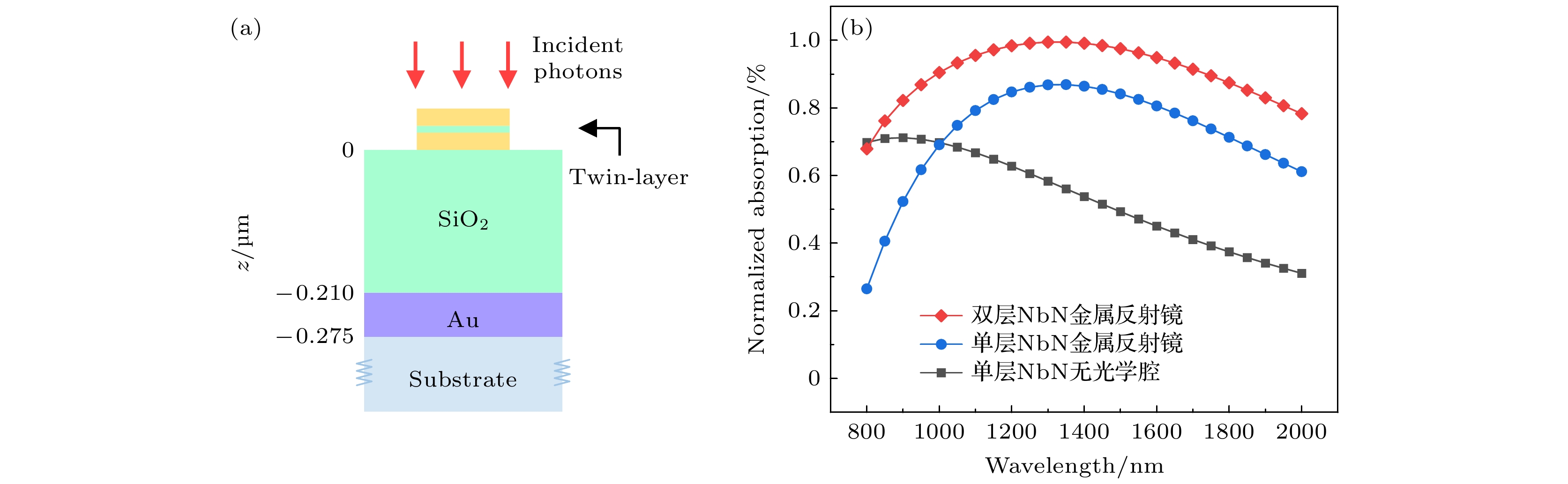
图 1 (a) 器件仿真模型; (b) 3种不同结构的纳米线在入射光800—2000 nm波段的光吸收仿真情况
Fig. 1. (a) Device simulation model; (b) the optical absorption simulation of three kinds of nanowires with different structures at 800–2000 nm wavelength of incident light.
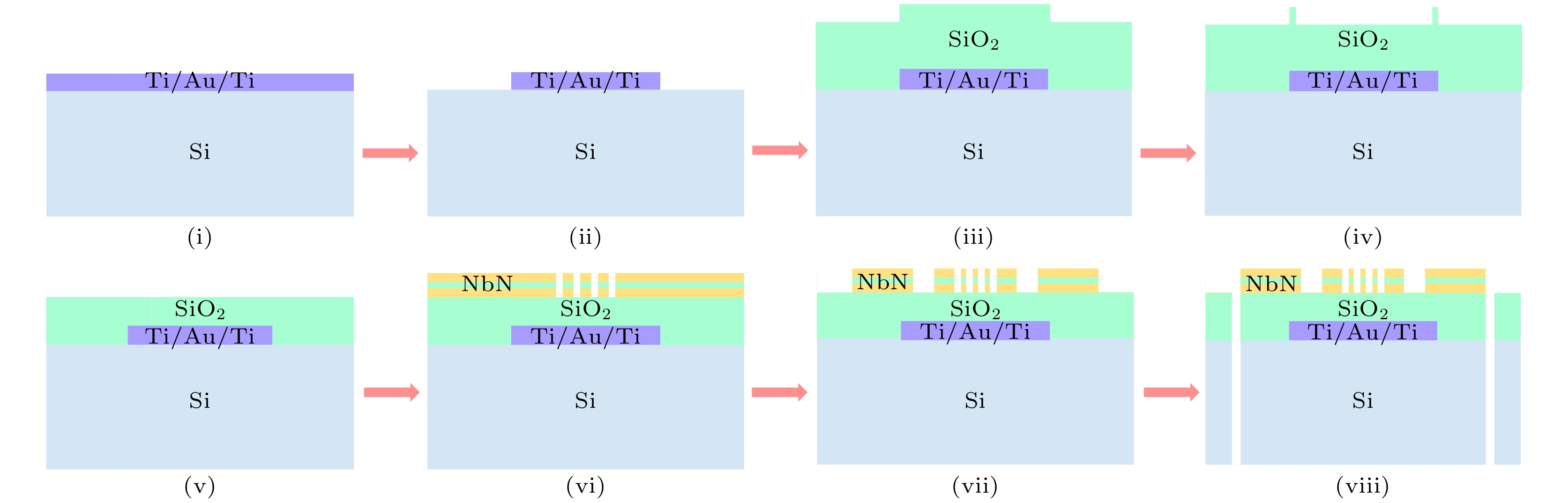
图 2 器件加工工艺流程图 (i) 通过磁控溅射法生长Ti/Au/Ti金属镜; (ii) 光刻后通过IBE法刻蚀金属镜; (iii) 采用PECVD法生长SiO2层; (iv) 光刻后采用RIE法刻蚀SiO2层; (v) 对SiO2进行化学机械抛光; (vi) 通过磁控溅射法生长上下两层NbN薄膜, PECVD法生长中间SiO2夹层, 并通过EBL曝光、RIE刻蚀制备纳米线条; (vii) 光刻后通过RIE法刻蚀NbN制备电极; (viii) 光刻后通过RIE法刻蚀SiO2阻挡层、ICP法刻蚀Si衬底获得自对准芯片
Fig. 2. Process flow chart (i) Ti/Au/Ti metal mirror is grown by magnetron sputtering; (ii) metal mirror is etched by the IBE process after lithography; (iii) SiO2 layer is grown by PECVD process; (iv) SiO2 layer is etched by RIE process after lithography; (v) chemical mechanical polishing of SiO2 layer; (vi) the upper and lower NbN layers are grown by magnetron sputtering, and the intermediate SiO2 layer is grown by PECVD process, and the nanowires are prepared by EBL exposure and RIE etching. (vii) the electrode is prepared by etching the NbN by RIE process after lithography; (viii) SiO2 layer is etched by RIE process and Si substrate is etched by ICP process after lithography to obtain self-aligned chips.
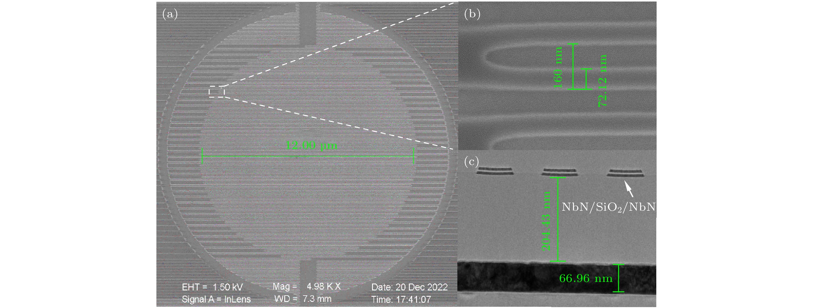
图 3 (a) 器件光敏面SEM图; (b) 高度放大的NbN纳米线SEM图; (c)器件横截面TEM图
Fig. 3. (a) SEM image of the active area of the device; (b) SEM image zoomed in on the NbN nanowires; (c) TEM image of the cross section of the nanowires.
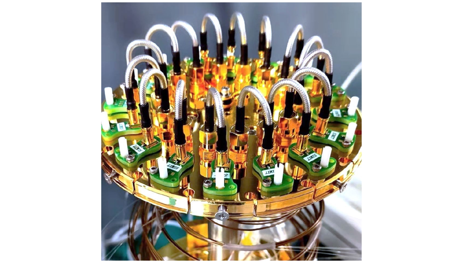
图 4 封装好的探测器芯片放置在恒温器的4 K冷台上
Fig. 4. The packaged chips are mounted on the 4 K cold plate.
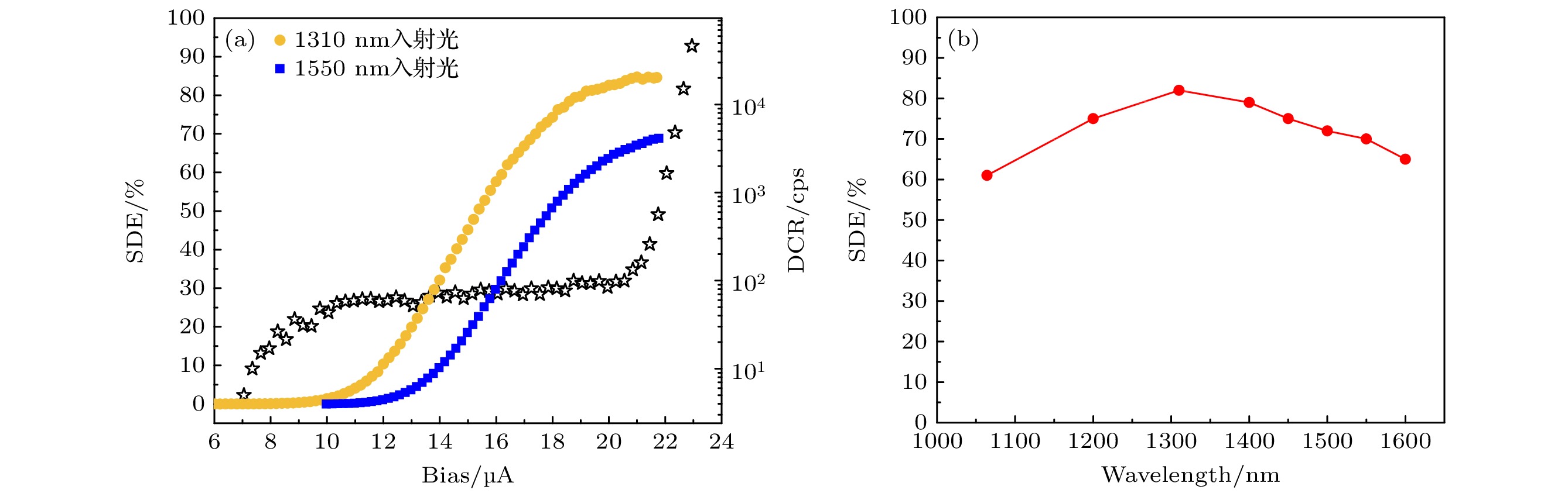
图 5 (a) 器件探测效率和暗计数率随偏置电流的变化曲线; (b) 器件在入射光1064—1600 nm波段的探测效率
Fig. 5. (a) SDE and DCR as a function of the bias currents; (b) SDE of the device at 1064–1600 nm.
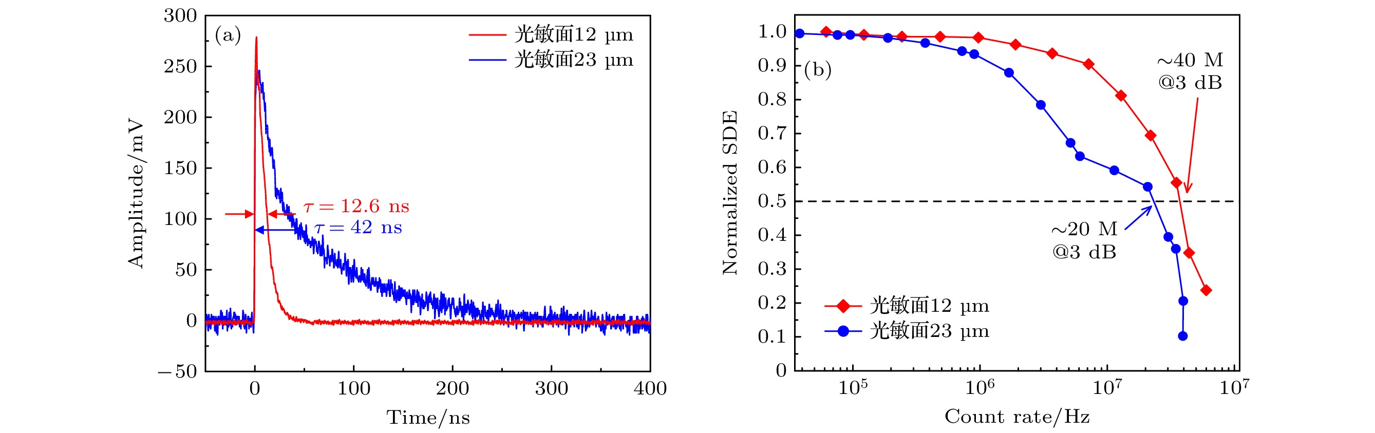
图 6 (a) 12 μm光敏面器件和23 μm光敏面器件响应波形和恢复时间; (b) 12 μm光敏面器件和23 μm光敏面器件归一化探测效率随入射光子数的变化曲线
Fig. 6. (a) Response waveform and recovery time of 12 μm active area device and 23 μm active area device; (b) curves of normalized detection efficiency of 12 μm active area device and 23 μm pactive area device with the number of incident photons.
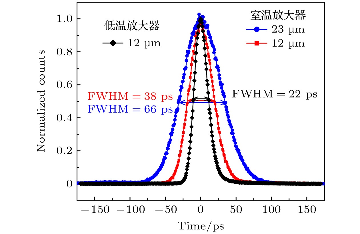
图 7 采用室温放大器放大输出信号时23 μm光敏面器件(蓝)、12 μm光敏面器件(红)的时间抖动与采用低温放大器放大输出信号时12 μm光敏面器件(黑)的时间抖动
Fig. 7. The timing jitter of 23 μm active area device (blue) and 12 μm active area device (red) when the output signal was amplified by room temperature amplifier respectively, and the timing jitter of 12 μm active area device (black) when the output signal was amplified by cryogenic amplifier.
-
[1] Zhang W J, You L X, Li H, Huang J, Lv C L, Zhang L, Liu X Y, Wu J J, Wang Z, Xie X M 2017 Sci. China-Phys. Mech. Astron. 60 1
[2] Zhang W J, Yang X Y, Li H, You L X, Lv C L, Zhang L, Zhang C J, Liu X Y, Wang Z, Xie X M 2018 Supercond. Sci. Technol. 31 035012
Google Scholar
[3] Knehr E, Kuzmin A, Doerner S, Wuensch S, Ilin K, Schmidt H, Siegel M 2020 Appl. Phys. Lett. 117 132602
Google Scholar
[4] Esmaeil Z I, Los J W N, Gourgues R B M, Chang J, Elshaari A W, Zichi J R, van Staaden Y J, Swens J P E, Kalhor N, Guardiani A, Meng Y, Zou K, Dobrovolskiy S, Fognini A W, Schaart D R, Dalacu D, Poole P J, Reimer M E, Hu X, Pereira S F, Zwiller V, Dorenbos S N 2020 ACS Photon. 7 1780
Google Scholar
[5] Khatri F I, Robinson B S, Semprucci M D, Boroson D M 2015 Acta Astronaut. 111 77
Google Scholar
[6] Zhong H S, Wang H, Deng Y H, Chen M C, Peng L C, Luo Y H, Qin J, Wu D, Ding X, Hu Y, Hu P, Yang X Y, Zhang W J, Li H, Li Y, Jiang X, Gan L, Yang G, You L, Wang Z, Li L, Liu N L, Lu C Y, Pan J W 2020 Science 370 1460
Google Scholar
[7] Zhang B, Guan Y Q, Xia L, Dong D, Chen Q, Xu C, Wu C, Huang H, Zhang L, Kang L, Chen J, Wu P 2021 Supercond. Sci. Tech. 34 034005
Google Scholar
[8] You L 2020 Nanophotonics 9 2673
Google Scholar
[9] 孙伟, 贾小氢, 涂学凑, 赵清源, 张蜡宝, 康琳, 陈健, 吴培亨 2022 低温与超导 50 9
Google Scholar
Sun W, Jia X H, Tu X C, Zhao Q Y, Zhang L B, Kang L, Chen J, Wu P H 2022 Cryog. Supercond. 50 9
Google Scholar
[10] Calandri N, Zhao Q Y, Zhu D, Dane A, Berggren K K 2016 Appl. Phys. Lett. 109 152601
Google Scholar
[11] Semenov A, Günther B, Böttger U, Hübers H W, Bartolf H, Engel A, Schilling A, Ilin K, Siegel M, Schneider R, Gerthsen D, Gippius N A 2009 Phys. Rev. B 80 054510
Google Scholar
[12] Banerjee A, Heath R M, Morozov D, Hemakumara D, Nasti U, Thayne I, Hadfield R H 2018 Opt. Mater. Express 8 2072
Google Scholar
[13] Gol’tsman G N, Okunev O, Chulkova G, Lipatov A, Semenov A, Smirnov K, Voronov B, Dzardanov A, Williams C, Sobolewski R 2001 Appl. Phys. Lett. 79 705
Google Scholar
[14] Semenov A, Engel A, Hubers H W, Il'in K, Siegel M 2005 Eur. Phys. J. B 47 495
Google Scholar
[15] Yang J K W, Kerman A J, Dauler E A, Anant V, Rosfjord K M, Berggren K K 2007 IEEE Trans. Appl. Supercon. 17 581
Google Scholar
[16] Kerman A J, Yang J K W, Molnar R J, Dauler E A, Berggren K K 2009 Phys. Rev. B 79 100509
Google Scholar
[17] Kerman A J, Dauler E A, Keicher W E, Yang J K W, Berggren K K, Gol’tsman G, Voronov B 2006 Appl. Phys. Lett. 88 111116
Google Scholar
[18] Allmaras J P, Kozorezov A G, Korzh B A, Berggren K K, Shaw M D 2019 Phys. Rev. Appl. 11 034062
Google Scholar
[19] Reddy D V, Nerem R R, Nam S W, Mirin R P, Verma V B 2020 Optica 7 1649
Google Scholar
[20] Chang J, Los J W N, Tenorio P J O, Noordzij N, Gourgues R, Guardiani A, Zichi J R, Pereira S F, Urbach H P, Zwiller V, Dorenbos S N, Esmaeil Zadeh I 2021 APL Photonics 6 036114
Google Scholar
[21] Meng Y, Zou K, Hu N, Xu L, Lan X, Steinhauer S, Gyger S, Zwiller V, Hu X J 2020 arXiv: 2012.06730
[22] Miki S, Yamashita T, Fujiwara M, Sasaki M, Wang Z 2010 Opt. Lett. 35 2133
Google Scholar
[23] Miller A J, Lita A E, Calkins B, Vayshenker I, Gruber S M, Nam S W 2011 Opt. Express 19 9102
Google Scholar
[24] Zadeh I E, Los J W N, Gourgues R B M, Steinmetz V, Bulgarini G, Dobrovolskiy S M, Zwiller V, Dorenbos S N 2017 APL Photonics 2 111301
Google Scholar
[25] Hu P, Li H, You L, Wang H, Xiao Y, Huang J, Yang X, Zhang W, Wang Z, Xie X 2020 Opt. Express 28 36884
Google Scholar
[26] 耿荣鑫, 李浩, 黄佳, 胡鹏, 肖游, 余慧勤, 尤立星 2021 激光与光电子学进展 58 285
Google Scholar
Geng R X, Li H, Huang J, Hu P, Xiao Y, Yu H Q, You L X 2021 Laser Optoelectron. Pro. 58 285
Google Scholar

 下载:
下载:
计量
- 文章访问数: 2343
- PDF下载量: 141
- 被引次数: 0
