


-
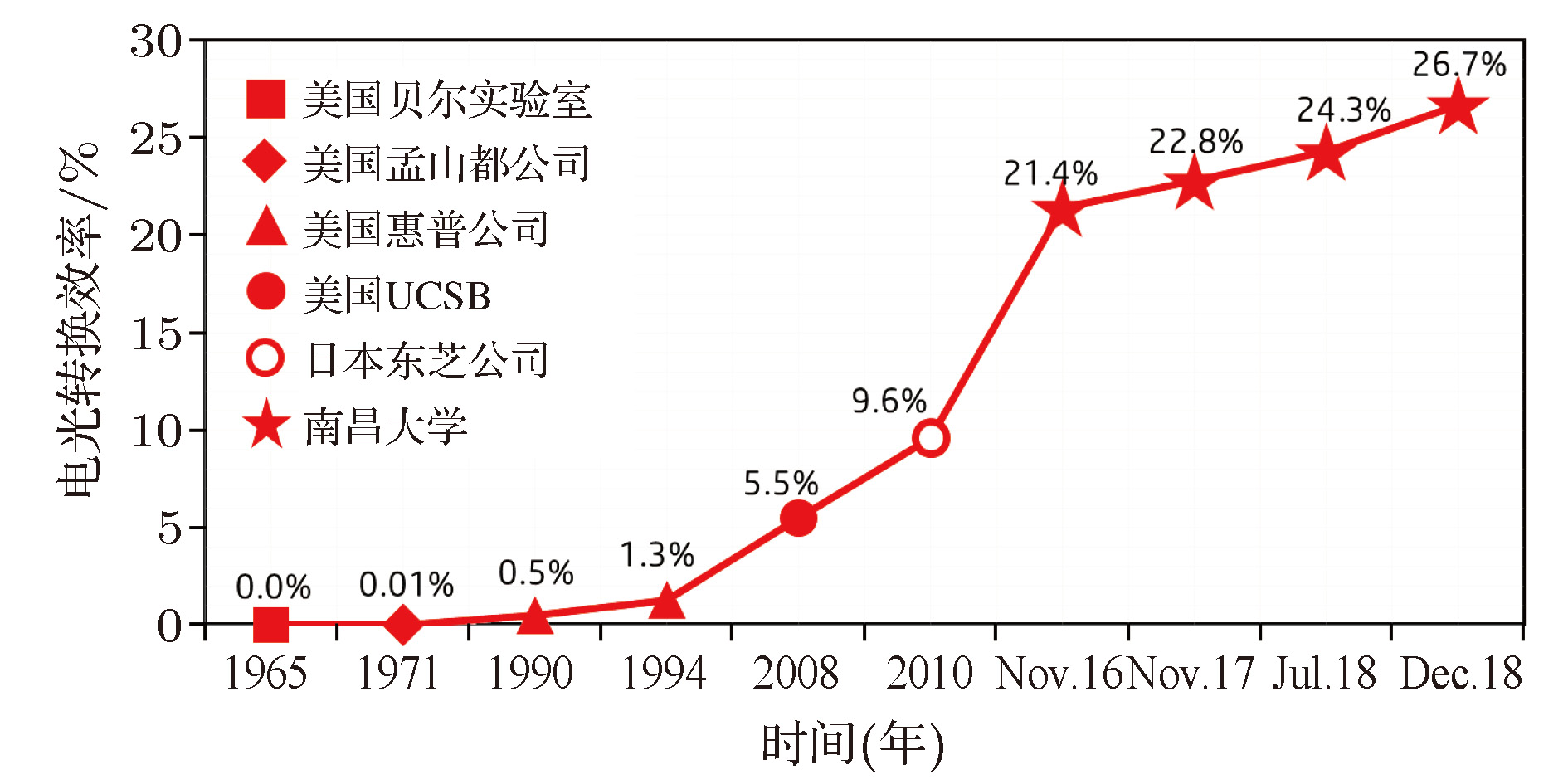
在可见光范围内, 半导体发光二极管(LED)发展很不平衡, 黄光LED光效(光功率效率)长期远低于其他颜色光效. 本文基于GaN/Si体系, 从材料生长、芯片制造、器件物理和专用装备等方面进行了系统研究, 解决了外延膜龟裂、位错过多、量子阱应力过大、InGaN黄光阱材料相分离、空穴浓度不足、阱材料生长温度过低、衬底吸光、电极挡光等问题, 率先实现了高光效黄光LED关键性突破. 所研制的黄光LED器件, 在20 A/cm2驱动下波长565 nm黄光LED光效达26.7%, 对应164 lm/W; 在1 A/cm2驱动下波长577 nm黄光LED光效达42.8%, 对应248 lm/W. 基于高光效黄光LED, 开发了无荧光粉、多基色LED照明新光源, 实现了纯LED照明光源在路灯、氛围灯等方面应用.
-
关键词:
- Si /
- InGaN /
- 黄光LED /
- 金属有机物化学气相沉积
The development of semiconductor light-emitting diode (LED) in the visible emission range is very unbalance, as the power efficiency of yellow LED is far below other colors. Based on the GaN/Si technology, the authors and his team made a systematic research from the aspect of material growth, chip fabrication, device physics and equipment design, resolved the problems of epi-film cracking, high dislocation density, large strain in quantum well (QW), phase separation in QW, low QW growth temperature, low hole concentration, light absorption by substrate and light blocking by electrode, successfully made a breakthrough in fabricating efficient yellow LED. The yellow LED chip achieves a power efficiency of 26.7% at 20 A/cm2 with 565 nm wavelength and efficacy of 164 lm/W, and the power efficiency goes up to 42.8% at 1 A/cm2 with 577 nm wavelength and efficacy of 248 lm/W. New LED light source with multi-colors and without phosphor was developed based on the efficient yellow LEDs, opened up a new direction of pure LED healthy lighting.-
Keywords:
- Si /
- InGaN /
- yellow light-emitting diode /
- metal-organic chemical vapor deposition
[1] Thomas D G, Hopfield J J 1966 Phys. Rev. 150 680
 Google Scholar
[2] Damilano B, Gil B 2015 J. Phys. D: Appl. Phys. 48 403001
Google Scholar
[3] Groves W O, Herzog A H, Craford M G 1971 Appl. Phys. Lett. 19 184
Google Scholar
[4] Kuo C P, Fletcher R M, Osentowski T D, Lardizabal M C, Craford M G, Robbins V M 1990 Appl. Phys. Lett. 57 2937
Google Scholar
[5] Kish F A, Steranka F M, DeFevere D C, van der Water D A, Park K G, Kuo C P, Osentowski T D, Peanasky M J, Yu J G, Fletcher R M, Steigerwald D A, Craford M G 1994 Appl. Phys. Lett. 64 2839
Google Scholar
[6] Satoa H, Chung R B, Hirasawa H, Fellows N, Masui H, Wu F, Saito M, Fujitob K, Speck J S, DenBaars S P, Nakamura S 2008 Appl. Phys. Lett. 92 221110
Google Scholar
[7] Saito S, Hashimoto R, Hwang J, Nunoue S 2013 Appl. Phys. Express 6 207
[8] Gessmann Th 2004 J. Appl. Phys. 95 2203
Google Scholar
[9] El-Masry N A, Piner E L, Liu S X, et al. 1998 Appl. Phys. Lett 72 40
Google Scholar
[10] Braslau N, Cuomo J, Harris P, et al. 1973 US patent 3849707
[11] Butter E, Fitzl G, Hirsch D, et al. 1979 Thin Solid Films 59 25
Google Scholar
[12] Takeuchi T, Amano H, Hiramatsu K, et al. 1991 J. Cryst. Growth 115 634
Google Scholar
[13] Watanabe A, Takeuchi T, Hirosawa K, et al. 1993 J. Cryst. Growth 128 391
Google Scholar
[14] Yang J, Sun C, Chen Q, et al. 1996 Appl. Phys. Lett. 69 3566
Google Scholar
[15] Kobayashi N, Kobayashi J, Dapkus P, et al. 1997 Appl. Phys. Lett. 71 3569
Google Scholar
[16] Wang L, Liu X, Zan Y, et al 1998 Appl. Phys. Lett. 72 109
Google Scholar
[17] Boo J, Rohr C, Ho W 1998 J. Cryst. Growth 189−190 439
[18] Guha S, Bojarczuk N 1998 Appl. Phys. Lett. 72 415
Google Scholar
[19] 江风益, 方文卿, 王立, 莫春兰, 刘和初, 周毛兴 2006 中国专利ZL200610072230.4
Jiang F Y, Fang W Q, Wang L, Mo C L, Liu H C, Zhou M X 2006 Chinese Patent ZL200610072230.4 (in Chinese)
[20] Mo C L, Fang W Q, PuY, Liu H C, Jiang F Y 2005 J. Cryst. Growth 285 312
Google Scholar
[21] Li T K, Mastro M, Dadgar A 2011 III-V Compound Semiconductors, Integration with Silicon-Based Microelectronics (CRC Press) p107
[22] Zhang J L, Xiong C B, Liu J L, Quan Z J, Wang L, Jiang F Y 2014 Appl. Phys. A 114 1049
Google Scholar
[23] Liu J L, Zhang J L, Mao Q H, Wu X M, Jiang F Y 2013 CrystEngComm 15 3372
Google Scholar
[24] 江风益, 刘军林, 王立, 等 2015 中国科学: 物理学 力学 天文学 45 067302
Jiang F Y, Liu J L, Wang L, et al. 2015 Sci. China: Phys. Mech. Astron. 45 067302
[25] Wu X H, Elsass C R, Abare A, et al 1998 Appl. Phys. Lett. 72 692
Google Scholar
[26] Hangleiter A, Hitzel F, Netzel C, Fuhrmann D, Rossow U, Ade G, Hinze P 2005 Phys. Rev. Lett. 95 127402
Google Scholar
[27] Wu X, Liu J, Quan Z, Xiong C, Zheng C, Zhang J, Mao Q, Jiang F 2014 Appl. Phys. Lett. 104 221101
Google Scholar
[28] Quan Z, Wang L, Zheng C, Liu J, Jiang F 2014 J. Appl. Phys. 116 183107
Google Scholar
[29] Wu X, Liu J, Jiang F 2015 J. Appl. Phys. 118 164504
Google Scholar
[30] Quan Z, Liu J, Fang F, Wang G, Jiang F 2015 J. Appl. Phys. 118 193102
Google Scholar
[31] Jiang F Y, Zhang J L, Xu L Q, et al. 2019 Photon. Res. 7 144
Google Scholar
[32] 江风益, 蒲勇 2004 中国专利 ZL200410017471.X.
Jiang F Y, Pu Y 2004 Chinese Patent ZL200410017471.X. (in Chinese)
[33] Jiang F Y, Zhang J L, Sun Q, Quan Z J2019 in Li J M, Zhang G Q ed. GaN LEDs on Si Substrate, Light-Emitting Diodes, Materials, Processes, Devices and Applications (Springer)pp133−170.
[34] Jiang F Y 2018 in Bi W G, Kuo H Z, Ku P C, Shen B ed., Advanced Optoelectronic Device Processing, Handbook of GaN Semiconductor Materials and Devices (CRC Press) pp285−304.
[35] Lin J, Ding X, Hong C, et al. 2019 Scientific Reports 9 7560
Google Scholar
-
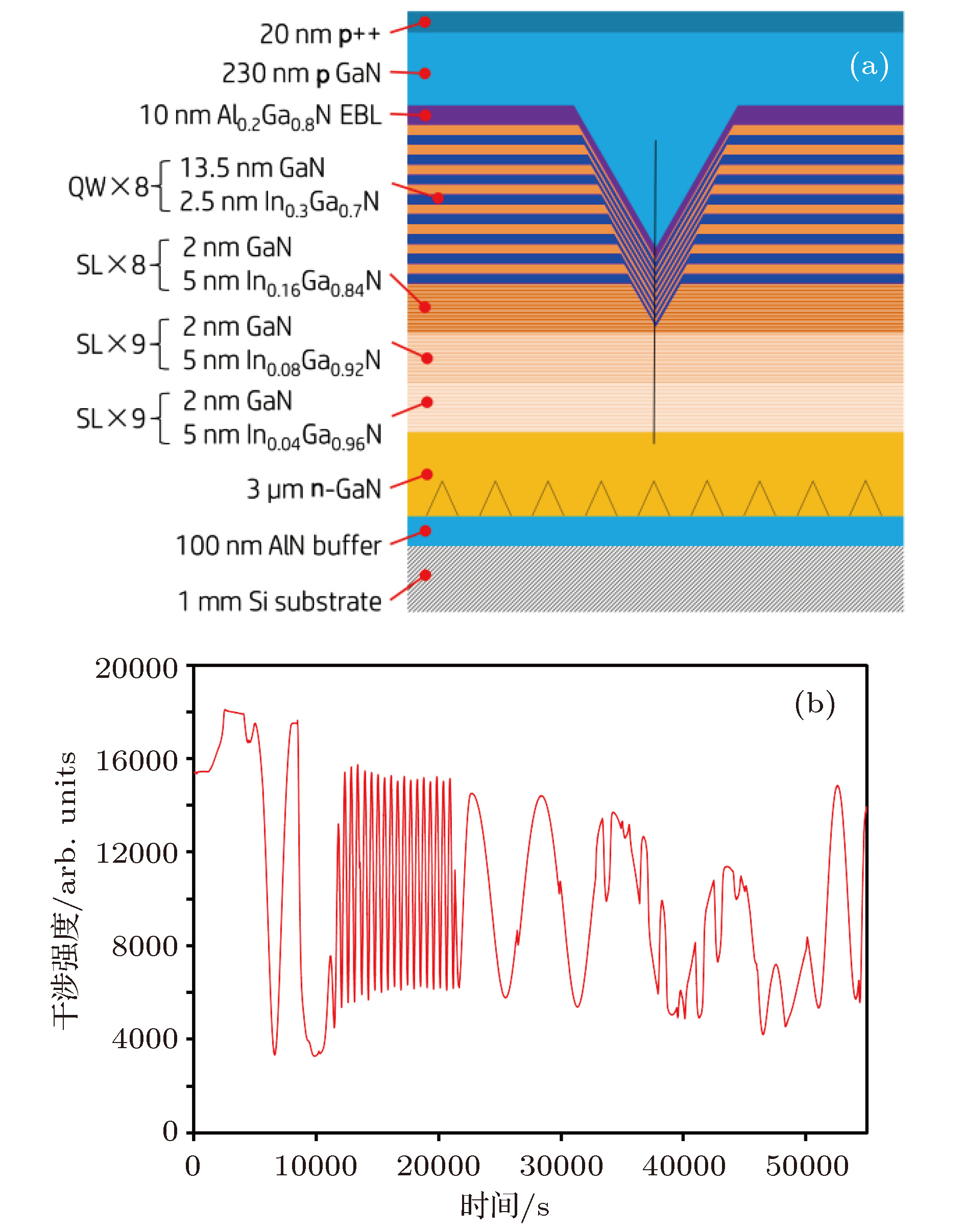
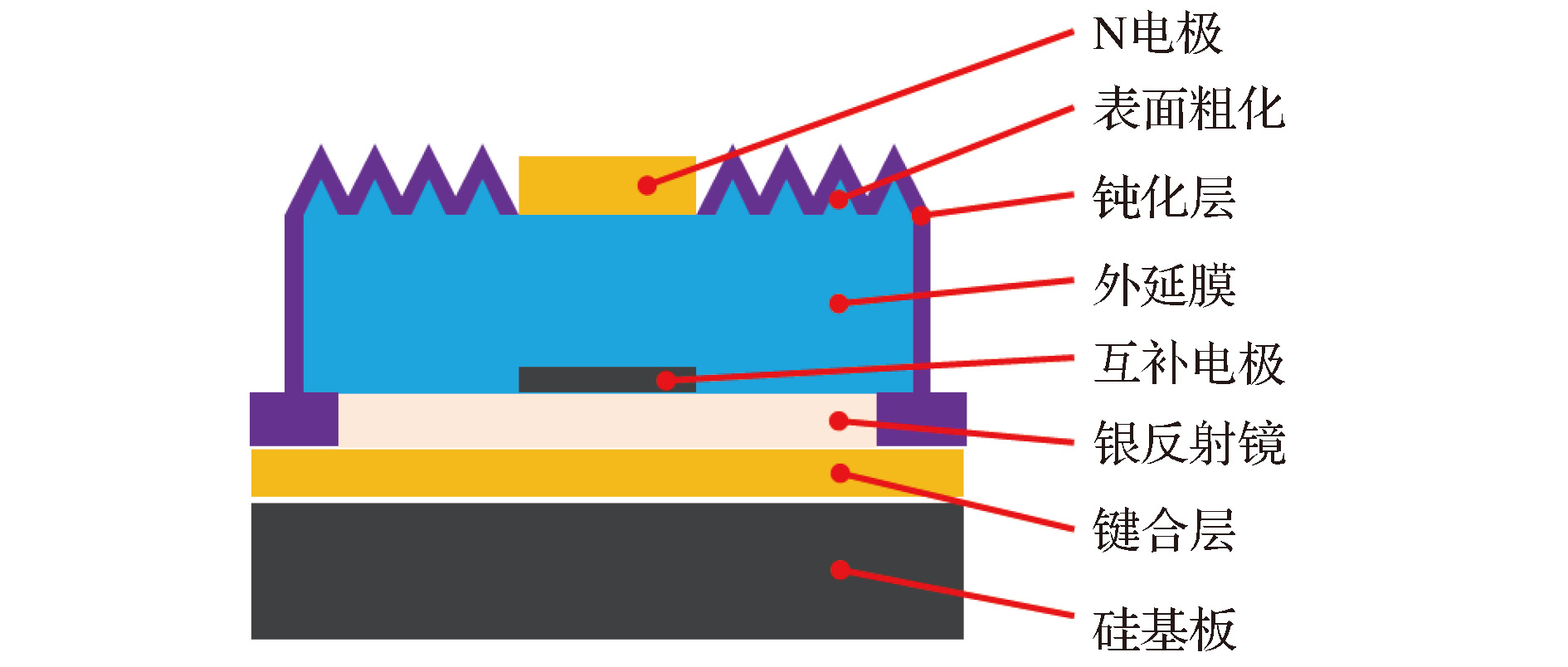
图 2 GaN/Si基黄光LED (a)外延材料结构示意图; (b)外延生长在线干涉曲线
Fig. 2. (a) Schematic structure and (b) in-situ interference curve of GaN based yellow LED on Si substrate
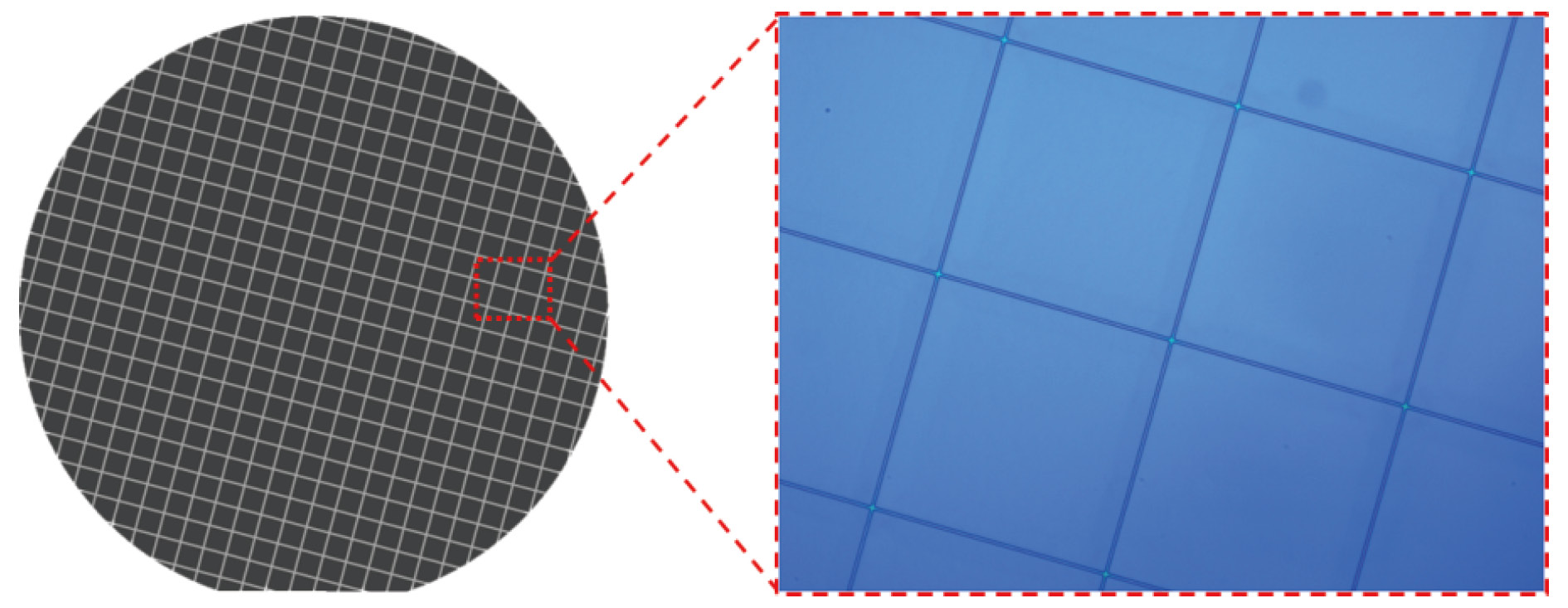
图 3 GaN/Si基LED外延材料网格化选区生长方法示意图
Fig. 3. Schematic of grid patterned Si substrate with GaN film grown on it
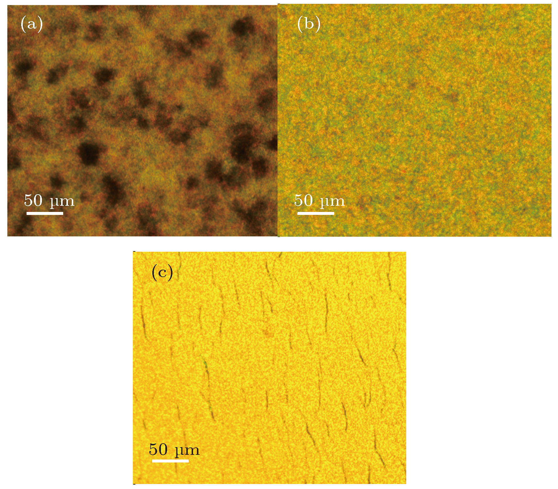
图 4 不同准备层的黄光LED量子阱荧光显微镜形貌 (a)无准备层; (b)单一In组分超晶格准备层; (c)三段In组分逐步提升的超晶格准备层
Fig. 4. Fluorescent luminescence (FL) spectrometry of yellow LED quantum well: (a) Without prestrained layer; (b) with fixed indium content prestrained SLS layers; (c) with three steps of increased indium content prestrained SLS layers
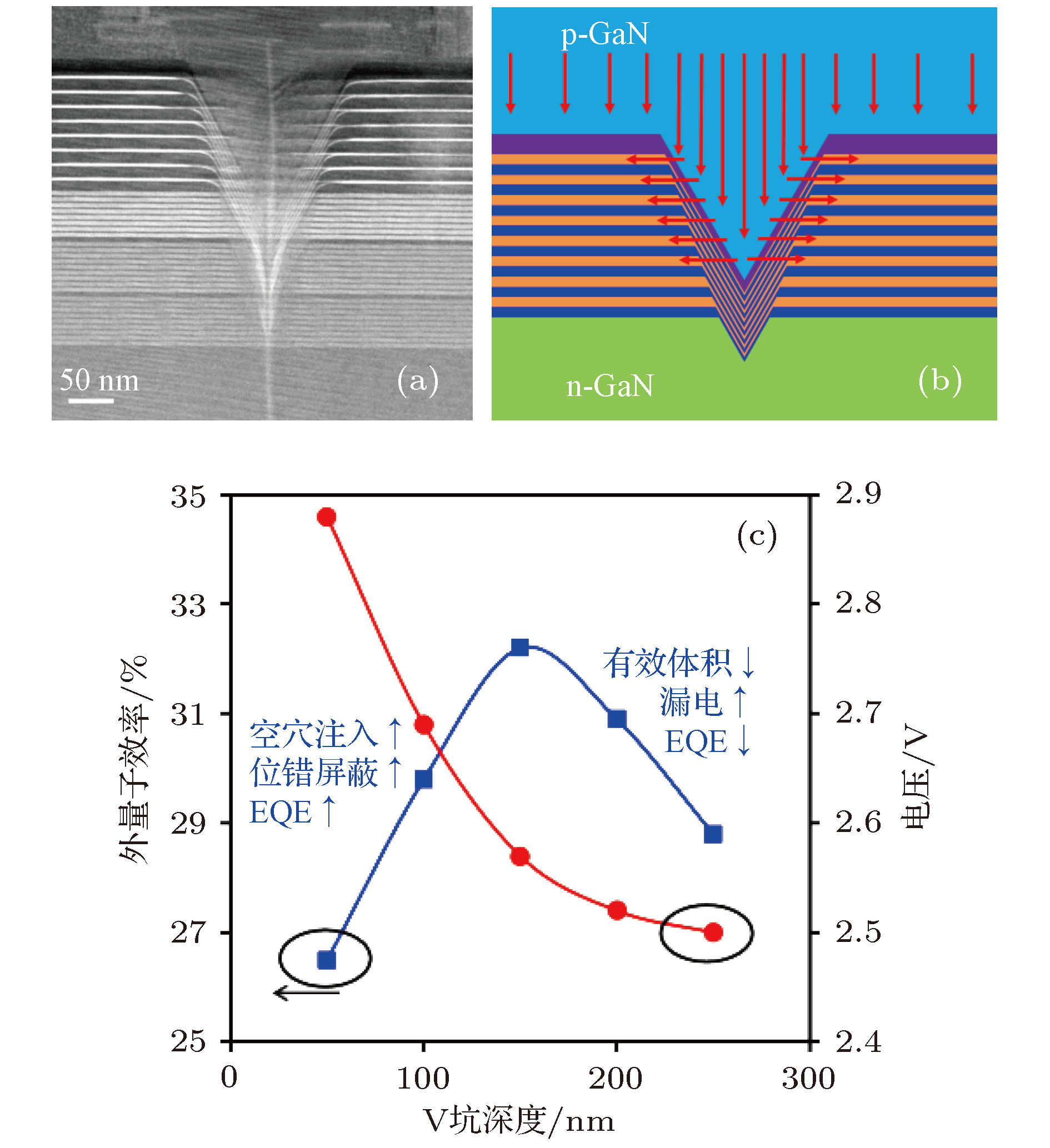
图 5 (a)含有V坑的黄光LED多量子阱结构透射电镜图; (b) V坑增强空穴注入示意图; (c)室温20 A/cm2下黄光LED外量子效率以及电压随V坑深度变化曲线
Fig. 5. (a) TEM image of yellow MQWs structure with V-pits; (b) schematic of hole injection enhancement by V-pits; (c) dependence of external quantum efficiency and voltage on V-pits size of yellow LED with 20 A/cm2 at room temperature
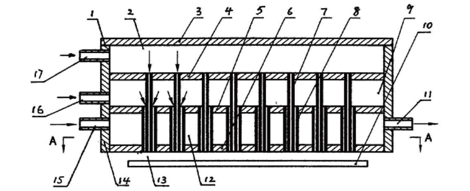
图 6 发明的专用MOCVD设备反应管气体输运结构-同轴套管喷头示意图
Fig. 6. The showerhead structure of self-designed MOCVD for yellow LED
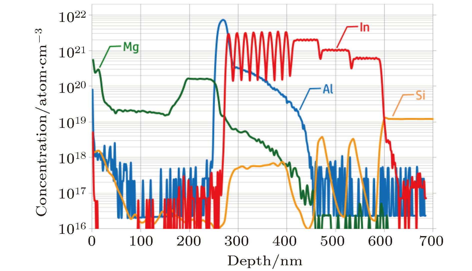
图 7 自制MOCVD设备生长的黄光LED材料的SIMS曲线
Fig. 7. SIMS profile of yellow LED structure grown by self-designed MOCVD

图 9 黄光LED样品B (a)室温不同电流下发光光谱; (b)变温变电流内量子效率曲线
Fig. 9. Electroluminescence of 565 nm yellow LED: (a) The room temperature emission spectrum at different current; (b) the internal quantum efficiency at various temperature and current density

图 10 无荧光粉LED照明光源电致发光光谱图 (a)蓝、青、绿、黄、红五基色白光LED; (b)黄、红光组成的金黄光LED
Fig. 10. EL spectra of phosphor free LEDs: (a) Color mixing white LED with blue, cyan, green, yellow and red LEDs; (b) golden light LEDs with yellow and red LEDs
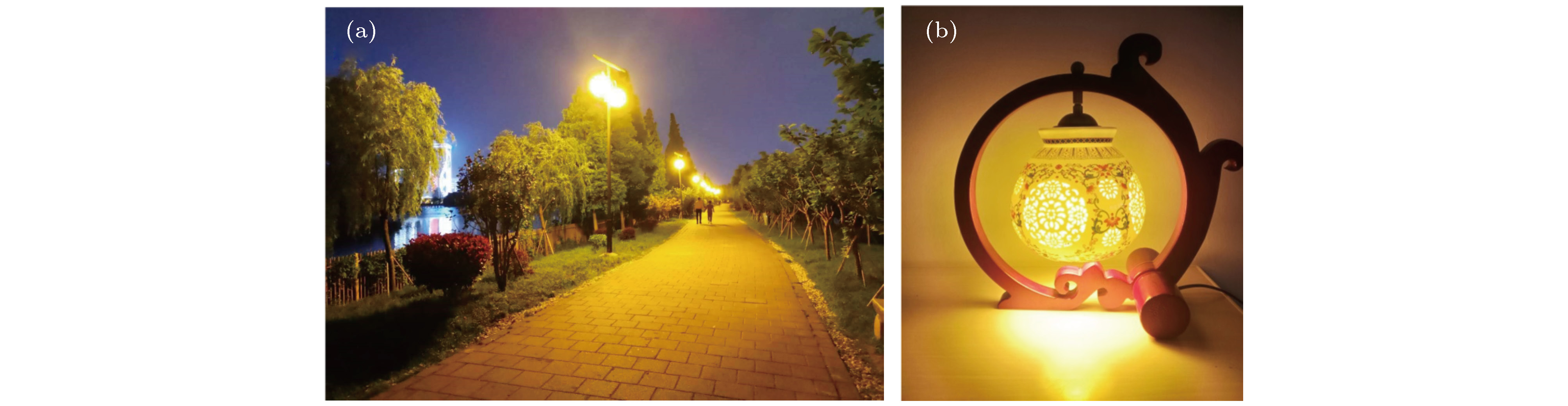
图 11 金黄光LED照明应用 (a)户外路灯(南昌市艾溪湖公园); (b)室内氛围台灯
Fig. 11. Applications of golden light LEDs as (a) Outdoor street lights and (b) indoor atmosphere lamps
表 1 黄光LED器件(芯片1 mm2)室温稳流状态电致发光结果
Table 1. Electroluminescence results of yellow LEDs (size 1 mm2) at room temperature and continues wave mode
样品 电流密度/A·cm–2 电流/mA 电压/V 主波长/nm 半宽/nm 光功率/mW 外量子效率/% 光功率效率/% 流明效率/lm·W–1 A 1 10 2.10 571 36.2 10.1 46.3 47.9 283 20 200 2.43 560 36.8 143.3 32.3 29.5 182 B 1 10 2.09 577 37.8 8.9 41.6 42.8 248 20 200 2.41 565 38.6 128.7 29.4 26.7 164 C 1 10 2.08 582 39.9 8.1 37.8 38.8 200 20 200 2.40 570 40.3 113.3 26.0 23.6 139  下载: 导出CSV
-
[1] Thomas D G, Hopfield J J 1966 Phys. Rev. 150 680
Google Scholar
[2] Damilano B, Gil B 2015 J. Phys. D: Appl. Phys. 48 403001
Google Scholar
[3] Groves W O, Herzog A H, Craford M G 1971 Appl. Phys. Lett. 19 184
Google Scholar
[4] Kuo C P, Fletcher R M, Osentowski T D, Lardizabal M C, Craford M G, Robbins V M 1990 Appl. Phys. Lett. 57 2937
Google Scholar
[5] Kish F A, Steranka F M, DeFevere D C, van der Water D A, Park K G, Kuo C P, Osentowski T D, Peanasky M J, Yu J G, Fletcher R M, Steigerwald D A, Craford M G 1994 Appl. Phys. Lett. 64 2839
Google Scholar
[6] Satoa H, Chung R B, Hirasawa H, Fellows N, Masui H, Wu F, Saito M, Fujitob K, Speck J S, DenBaars S P, Nakamura S 2008 Appl. Phys. Lett. 92 221110
Google Scholar
[7] Saito S, Hashimoto R, Hwang J, Nunoue S 2013 Appl. Phys. Express 6 207
[8] Gessmann Th 2004 J. Appl. Phys. 95 2203
Google Scholar
[9] El-Masry N A, Piner E L, Liu S X, et al. 1998 Appl. Phys. Lett 72 40
Google Scholar
[10] Braslau N, Cuomo J, Harris P, et al. 1973 US patent 3849707
[11] Butter E, Fitzl G, Hirsch D, et al. 1979 Thin Solid Films 59 25
Google Scholar
[12] Takeuchi T, Amano H, Hiramatsu K, et al. 1991 J. Cryst. Growth 115 634
Google Scholar
[13] Watanabe A, Takeuchi T, Hirosawa K, et al. 1993 J. Cryst. Growth 128 391
Google Scholar
[14] Yang J, Sun C, Chen Q, et al. 1996 Appl. Phys. Lett. 69 3566
Google Scholar
[15] Kobayashi N, Kobayashi J, Dapkus P, et al. 1997 Appl. Phys. Lett. 71 3569
Google Scholar
[16] Wang L, Liu X, Zan Y, et al 1998 Appl. Phys. Lett. 72 109
Google Scholar
[17] Boo J, Rohr C, Ho W 1998 J. Cryst. Growth 189−190 439
[18] Guha S, Bojarczuk N 1998 Appl. Phys. Lett. 72 415
Google Scholar
[19] 江风益, 方文卿, 王立, 莫春兰, 刘和初, 周毛兴 2006 中国专利ZL200610072230.4
Jiang F Y, Fang W Q, Wang L, Mo C L, Liu H C, Zhou M X 2006 Chinese Patent ZL200610072230.4 (in Chinese)
[20] Mo C L, Fang W Q, PuY, Liu H C, Jiang F Y 2005 J. Cryst. Growth 285 312
Google Scholar
[21] Li T K, Mastro M, Dadgar A 2011 III-V Compound Semiconductors, Integration with Silicon-Based Microelectronics (CRC Press) p107
[22] Zhang J L, Xiong C B, Liu J L, Quan Z J, Wang L, Jiang F Y 2014 Appl. Phys. A 114 1049
Google Scholar
[23] Liu J L, Zhang J L, Mao Q H, Wu X M, Jiang F Y 2013 CrystEngComm 15 3372
Google Scholar
[24] 江风益, 刘军林, 王立, 等 2015 中国科学: 物理学 力学 天文学 45 067302
Jiang F Y, Liu J L, Wang L, et al. 2015 Sci. China: Phys. Mech. Astron. 45 067302
[25] Wu X H, Elsass C R, Abare A, et al 1998 Appl. Phys. Lett. 72 692
Google Scholar
[26] Hangleiter A, Hitzel F, Netzel C, Fuhrmann D, Rossow U, Ade G, Hinze P 2005 Phys. Rev. Lett. 95 127402
Google Scholar
[27] Wu X, Liu J, Quan Z, Xiong C, Zheng C, Zhang J, Mao Q, Jiang F 2014 Appl. Phys. Lett. 104 221101
Google Scholar
[28] Quan Z, Wang L, Zheng C, Liu J, Jiang F 2014 J. Appl. Phys. 116 183107
Google Scholar
[29] Wu X, Liu J, Jiang F 2015 J. Appl. Phys. 118 164504
Google Scholar
[30] Quan Z, Liu J, Fang F, Wang G, Jiang F 2015 J. Appl. Phys. 118 193102
Google Scholar
[31] Jiang F Y, Zhang J L, Xu L Q, et al. 2019 Photon. Res. 7 144
Google Scholar
[32] 江风益, 蒲勇 2004 中国专利 ZL200410017471.X.
Jiang F Y, Pu Y 2004 Chinese Patent ZL200410017471.X. (in Chinese)
[33] Jiang F Y, Zhang J L, Sun Q, Quan Z J2019 in Li J M, Zhang G Q ed. GaN LEDs on Si Substrate, Light-Emitting Diodes, Materials, Processes, Devices and Applications (Springer)pp133−170.
[34] Jiang F Y 2018 in Bi W G, Kuo H Z, Ku P C, Shen B ed., Advanced Optoelectronic Device Processing, Handbook of GaN Semiconductor Materials and Devices (CRC Press) pp285−304.
[35] Lin J, Ding X, Hong C, et al. 2019 Scientific Reports 9 7560
Google Scholar

 下载:
下载:
计量
- 文章访问数: 11623
- PDF下载量: 225
- 被引次数: 0
