


-
本文在n-(Al0.27Ga0.73)0.5In0.5P表面通过电子束蒸发Ni/Au/Ge/Ni/Au叠层金属并优化退火工艺成功制备了具有较低接触电阻的欧姆接触, 其比接触电阻率在445 ℃退火600 s时达到1.4 × 10⁻⁴ Ω·cm2. 二次离子质谱仪测试表明, 叠层金属Ni/Au/Ge/Ni/Au与n-AlGaInP界面发生固相反应, Ga, In原子由于热分解发生外扩散并在晶格中留下Ⅲ族空位. 本文把欧姆接触形成的原因归结为Ge原子内扩散占据Ga空位和In空位作为施主提高N型掺杂浓度. 优化退火工艺对低掺杂浓度n-(Al0.27Ga0.73)0.5In0.5P的欧姆接触性能有显著改善效果, 但随着n-(Al0.27Ga0.73)0.5In0.5P掺杂浓度提高, 比接触电阻率与退火工艺没有明显关系. 本文为n面出光的AlGaInP薄膜发光二极管芯片的n电极制备提供了一种新的方法, 有望大幅简化制备工艺, 降低制造成本.In this paper, Ni/Au/Ge/Ni/Au laminated metals were deposited on the n-(Al0.27Ga0.73)0.5In0.5P by electron beam evaporation, the ohmic contact with low contact resistance was successfully prepared by optimized annealing process. The specific contact resistance reached 1.4 × 10⁻⁴ Ω·cm2 when annealed at 445 ℃ for 600 s. The result of the secondary ion mass spectrometer shows that the solid-state reaction takes place at the interface between the laminated metal Ni/Au/Ge/Ni/Au and n-AlGaInP, then the germanium atoms and indium atoms diffuse outwards due to thermal decomposition and leave vacancies in the lattice. In this paper, the reason for the formation of ohmic contact is attributed to the fact that the germanium vacancy and indium vacancy are occupied by gallium atoms as donors to increasing the N-type doping concentration. The optimized annealing process can improve the ohmic contact performance of n-(Al0.27Ga0.73)0.5In0.5P with low doping concentration, but the specific contact resistivity has no obvious relationship with the annealing process when the of doping concentration of n-(Al0.27Ga0.73)0.5In0.5P increased. The Schottky barrier is high at low doping concentration of n-(Al0.27Ga0.73)0.5In0.5P. So inter diffusion in the annealing process could significantly increase the doping concentration of n-(Al0.27Ga0.73)0.5In0.5P and reduce the Schottky barrier height. Nevertheless, the Schottky barrier of the sample with high doping concentration is low enough what is not sensitive with inter diffusion. It provides a new method for the preparation of N-electrode of AlGaInP thin film light-emitting-diodes chip, as so as avoid the problem of n+-GaAs absorption in the conventional N-electrode preparation method and the problem of electrode dropping. However, there are still some shortcomings in this paper. The disadvantage is that the high doping concentration of n-AlGaInP will affect the crystal quality, which will reduce the luminous efficiency of LED. Therefore, in order to prepare ohmic contact with excellent properties on n-AlGaInP with lower doping concentration, optimizing the electrode design and the surface treatment of semiconductor materials are the keys to follow-up research.
-
Keywords:
- AlGaInP /
- ohmic contact /
- annealing process /
- film chip
[1] Hong R H, Huang S H, Wu D S, Chi C Y 2003 Appl. Phys. Lett. 82 4011
 Google Scholar
[2] Gessmann T, Schubert E F 2004 J. Appl. Phys. 95 2203
Google Scholar
[3] Dupuis R D, Krames M R 2008 J. Lightwave. Technol. 26 1154
Google Scholar
[4] Kish F A, Steranka F M, Defevere D C, Vanderwater D A, Park K G, Kuo C P, Osentowski T D, Peanasky M J, Yu J G, Fletcher R M 1994 Appl. Phys. 64 2839
[5] 刘自可, 高伟, 徐晨 2010 半导体学报 31 52
Liu Z K, Gao W, Xu C 2010 J. Semicond. 31 52
[6] Huang W, Chien F S, Yen F, Lin C, Ching B, Chiang K N 2014 Solid. State. Electron. 93 15
Google Scholar
[7] Dong Y, Han J, Chen X, Xie Y, Jie S 2016 IEEE Electron Device Lett. 37 1303
Google Scholar
[8] 战瑛, 牛丽娟, 李晓云, 王小丽, 彭晓磊 2008 半导体技术 8 15
Google Scholar
Zhan Y, Niu L J, Li X Y, Wang X L, Peng X L 2008 Semicond. Technol. 8 15
Google Scholar
[9] Sai S G, Mahadeva B K, Dhamodaran S, Pathak A P, Muralidharan R, Vyas H P, Sridhara R D, Balamuralikrishnan R, Muraleedharan K 2015 Mater. Sci. Semicond. Process. 30 62
Google Scholar
[10] Carroll J E 1977 IET. Power. Electron. 23 841
[11] Tahamtan S, Goodarzi A, Abbasi S P, Hodaei A, Zabihi M S, Sabbaghzadeh J 2011 Microelectron. Reliab. 51 1330
Google Scholar
[12] Kumar D 2006 Phys. Status Solidi A 139 433
[13] Clausen T, Leistiko O 1995 Semicond. Sci. Technol. 10 691
Google Scholar
[14] 吴鼎芬, 王德宁 1985 物理学报 34 332
Google Scholar
Wu D F, Wang D N 1985 Acta. Phys. Sin. 34 332
Google Scholar
[15] 王光绪, 陶喜霞, 熊传兵, 刘军林, 封飞飞, 张萌, 江风益 2011 物理学报 60 808
Wang G X, Tao X X, Xiong C B, Liu J L, Feng F F, Zhang M, Jiang F Y 2011 Acta. Phys. Sin. 60 808
[16] Blank T V, Gol’Dberg Y A 2007 Semiconductors. 41 1263
Google Scholar
[17] 刘恩科, 朱秉升, 罗晋生 2011 半导体物理学 (第7版) (北京: 电子工业出版社) 第204页
Liu E K, Zhu B S, Luo J S 2011 The Physics of Semiconductors (7th Ed.) (Beijing: Electronics industry Press) p204 (in Chinese)
[18] Lumpkin N E, Lumpkin G R, Blackford M G 1999 J. Mater. Res. 14 1261
Google Scholar
[19] Hao P H, Wang L C, Ressel P, Kuo J M 1996 J. Vac. Sci. Technol., B 14 3244
Google Scholar
[20] 郭伟玲, 钱可元, 王军喜 2015 LED器件与工艺技术 (北京: 电子工业出版社) 第76页
Guo W L, Qian K W, Wang J X 2015 LED Devices and Technology (Beijing: Publishing House of Electronics Industry) p76 (in Chinese)
[21] Clausen T, Leistiko O, Chorkendorff I, Larsen J 1993 Thin Solid Films 232 215
Google Scholar
[22] Farmanbar M, Brocks G 2016 Adv. Electron. Mater. 2 4
[23] Wen C H, Tan F L, Lee C L 1996 J. Appl. Phys. 79 9200
Google Scholar
-
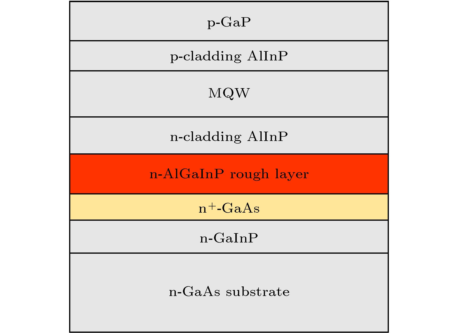
图 1 AlGaInP LED基本外延结构
Fig. 1. Schematic diagrams of AlGaInP-base LED epitaxial structure.
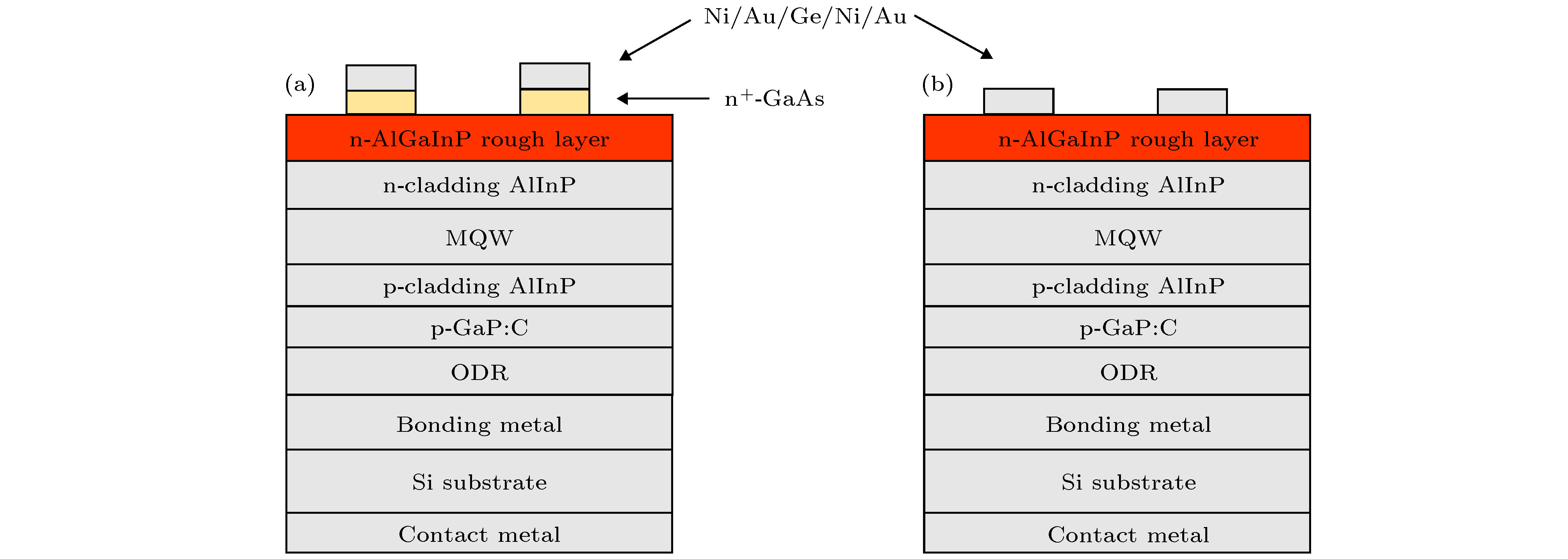
图 2 n面出光AlGaInP LED (a)常规结构薄膜芯片; (b)基于n-AlGaInP欧姆接触的芯片结构
Fig. 2. Schematic diagrams of (a) conventional n-side-up AlGaInP LED structure and (b) n-AlGaInP contact LED.

图 3 D5样品的I-V曲线, 圆环间距为10−35 µm
Fig. 3. I-V behaviors of Sample D5, ring intervals are 10−35 µm
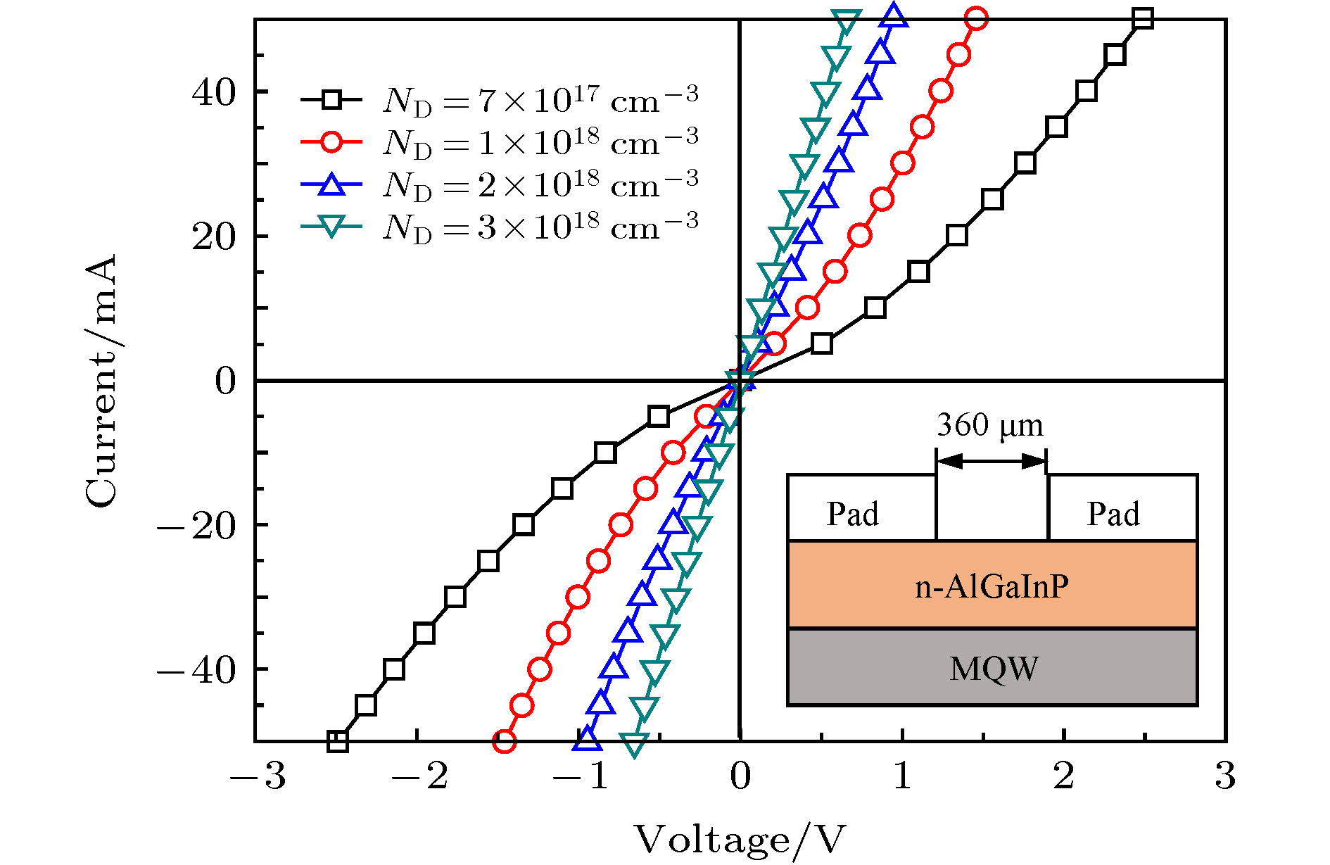
图 4 385 ℃退火25 s时, A1, B1, C1和D1样品I-V曲线
Fig. 4. I-V behaviors of Sample A1, B1, C1 and D1 after annealing at 385 ℃ for 25 s.
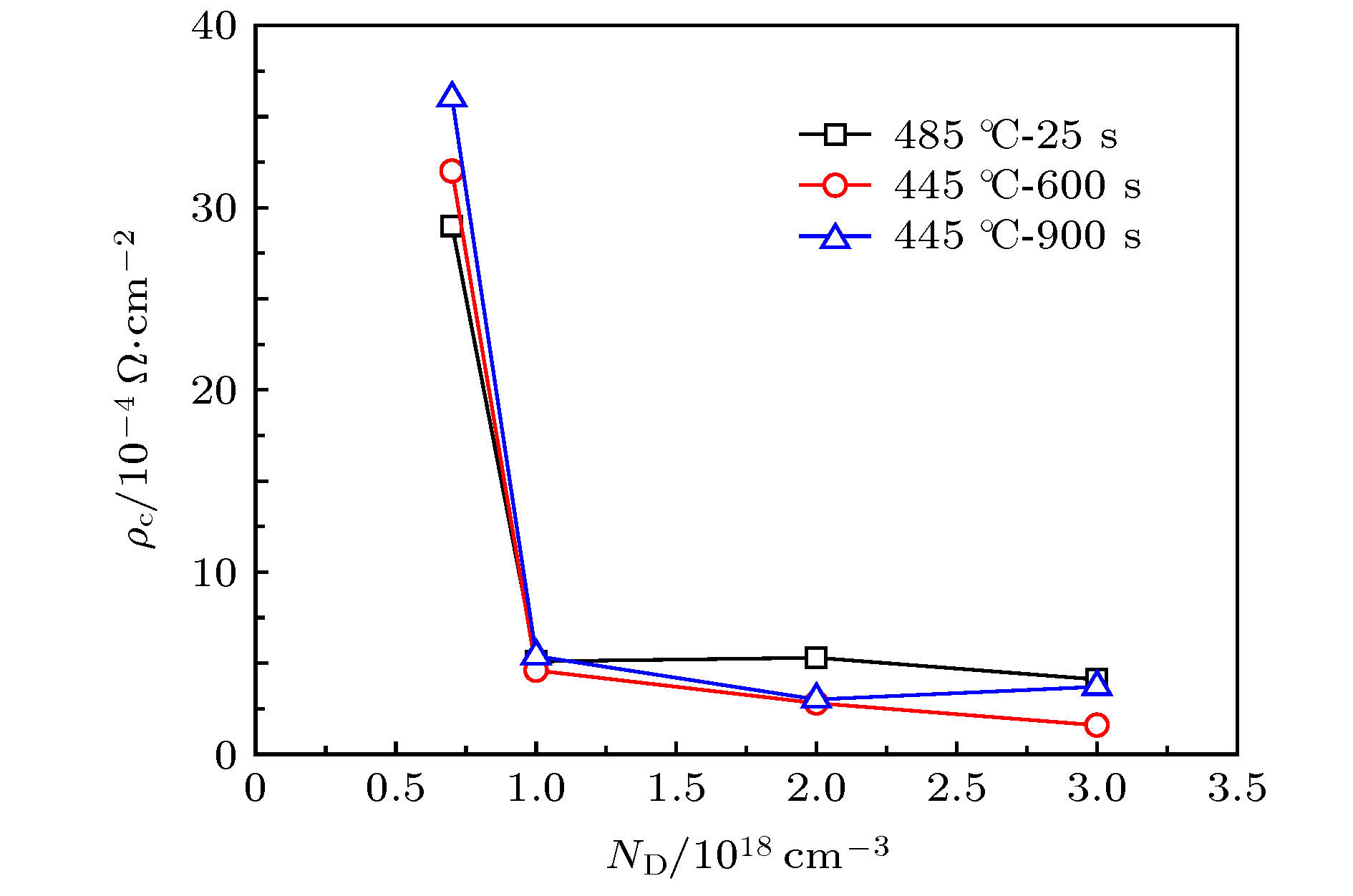
图 5 不同退火条件下, ρc与ND关系
Fig. 5. Contact resistivity as a function of doping concentration for different annealing conditions.

图 6 SIMS深度剖析Ni/Au/Ge/Ni/Au与n-(Al0.27Ga0.73)0.5In0.5P接触性能
Fig. 6. SIMS depth profiles of Ni/Au/Ge/Ni/Au contact on n-(Al0.27Ga0.73)0.5In0.5P before annealing and after annealing.

图 7 相同掺杂浓度时 (a)退火时间25 s, ρc与退火温度关系; (b) 退火温度445 ℃, ρc与退火时间关系
Fig. 7. At the same ND (a) ρc as a function of annealing temperature when the annealing time is 25 s; (b) ρc as a function of annealing temperature when the annealing temperature is 445 ℃.

图 8 SEM测试不同退火温度下接触界面形貌 (a) 445 ℃退火25 s; (b) 485 ℃退火25 s
Fig. 8. SEM micrographs showing the surface morphologies of ohmic contact (a) 445 ℃ for 25 s (b) 485 ℃ for 25 s.
表 1 样品退火分组信息及比接触电阻率(ρc)测试结果
Table 1. Grouping information of samples annealing and specific contact resistivity (ρc) results.
编号 ND/cm-3 T/℃ Time/s ρc/Ω·cm2 编号 ND/cm-3 T/℃ Time/s ρc/Ω·cm2 A1 7 × 10¹⁷ 385 25 — C1 2 × 10¹⁸ 385 25 1.1 × 10⁻³ A2 7 × 10¹⁷ 425 25 — C2 2 × 10¹⁸ 425 25 9.4 × 10⁻⁴ A3 7 × 10¹⁷ 445 25 — C3 2 × 10¹⁸ 445 25 4.8 × 10⁻⁴ A4 7 × 10¹⁷ 485 25 2.9 × 10⁻³ C4 2 × 10¹⁸ 485 25 5.3 × 10⁻⁴ A5 7 × 10¹⁷ 445 600 3.2 × 10⁻³ C5 2 × 10¹⁸ 445 600 2.8 × 10⁻⁴ A6 7 × 10¹⁷ 445 900 3.6 × 10⁻³ C6 2 × 10¹⁸ 445 900 3.0 × 10⁻⁴ B1 1 × 10¹⁸ 385 25 — D1 3 × 10¹⁸ 385 25 4.9 × 10⁻⁴ B2 1 × 10¹⁸ 425 25 — D2 3 × 10¹⁸ 425 25 4.0 × 10⁻⁴ B3 1 × 10¹⁸ 445 25 3.5 × 10⁻³ D3 3 × 10¹⁸ 445 25 3.3 × 10⁻⁴ B4 1 × 10¹⁸ 485 25 5.1 × 10⁻⁴ D4 3 × 10¹⁸ 485 25 4.1 × 10⁻⁴ B5 1 × 10¹⁸ 445 600 4.6 × 10⁻⁴ D5 3 × 10¹⁸ 445 600 1.4 × 10⁻⁴ B6 1 × 10¹⁸ 445 900 5.4 × 10⁻⁴ D6 3 × 10¹⁸ 445 900 1.9 × 10⁻⁴  下载: 导出CSV
-
[1] Hong R H, Huang S H, Wu D S, Chi C Y 2003 Appl. Phys. Lett. 82 4011
Google Scholar
[2] Gessmann T, Schubert E F 2004 J. Appl. Phys. 95 2203
Google Scholar
[3] Dupuis R D, Krames M R 2008 J. Lightwave. Technol. 26 1154
Google Scholar
[4] Kish F A, Steranka F M, Defevere D C, Vanderwater D A, Park K G, Kuo C P, Osentowski T D, Peanasky M J, Yu J G, Fletcher R M 1994 Appl. Phys. 64 2839
[5] 刘自可, 高伟, 徐晨 2010 半导体学报 31 52
Liu Z K, Gao W, Xu C 2010 J. Semicond. 31 52
[6] Huang W, Chien F S, Yen F, Lin C, Ching B, Chiang K N 2014 Solid. State. Electron. 93 15
Google Scholar
[7] Dong Y, Han J, Chen X, Xie Y, Jie S 2016 IEEE Electron Device Lett. 37 1303
Google Scholar
[8] 战瑛, 牛丽娟, 李晓云, 王小丽, 彭晓磊 2008 半导体技术 8 15
Google Scholar
Zhan Y, Niu L J, Li X Y, Wang X L, Peng X L 2008 Semicond. Technol. 8 15
Google Scholar
[9] Sai S G, Mahadeva B K, Dhamodaran S, Pathak A P, Muralidharan R, Vyas H P, Sridhara R D, Balamuralikrishnan R, Muraleedharan K 2015 Mater. Sci. Semicond. Process. 30 62
Google Scholar
[10] Carroll J E 1977 IET. Power. Electron. 23 841
[11] Tahamtan S, Goodarzi A, Abbasi S P, Hodaei A, Zabihi M S, Sabbaghzadeh J 2011 Microelectron. Reliab. 51 1330
Google Scholar
[12] Kumar D 2006 Phys. Status Solidi A 139 433
[13] Clausen T, Leistiko O 1995 Semicond. Sci. Technol. 10 691
Google Scholar
[14] 吴鼎芬, 王德宁 1985 物理学报 34 332
Google Scholar
Wu D F, Wang D N 1985 Acta. Phys. Sin. 34 332
Google Scholar
[15] 王光绪, 陶喜霞, 熊传兵, 刘军林, 封飞飞, 张萌, 江风益 2011 物理学报 60 808
Wang G X, Tao X X, Xiong C B, Liu J L, Feng F F, Zhang M, Jiang F Y 2011 Acta. Phys. Sin. 60 808
[16] Blank T V, Gol’Dberg Y A 2007 Semiconductors. 41 1263
Google Scholar
[17] 刘恩科, 朱秉升, 罗晋生 2011 半导体物理学 (第7版) (北京: 电子工业出版社) 第204页
Liu E K, Zhu B S, Luo J S 2011 The Physics of Semiconductors (7th Ed.) (Beijing: Electronics industry Press) p204 (in Chinese)
[18] Lumpkin N E, Lumpkin G R, Blackford M G 1999 J. Mater. Res. 14 1261
Google Scholar
[19] Hao P H, Wang L C, Ressel P, Kuo J M 1996 J. Vac. Sci. Technol., B 14 3244
Google Scholar
[20] 郭伟玲, 钱可元, 王军喜 2015 LED器件与工艺技术 (北京: 电子工业出版社) 第76页
Guo W L, Qian K W, Wang J X 2015 LED Devices and Technology (Beijing: Publishing House of Electronics Industry) p76 (in Chinese)
[21] Clausen T, Leistiko O, Chorkendorff I, Larsen J 1993 Thin Solid Films 232 215
Google Scholar
[22] Farmanbar M, Brocks G 2016 Adv. Electron. Mater. 2 4
[23] Wen C H, Tan F L, Lee C L 1996 J. Appl. Phys. 79 9200
Google Scholar

 下载:
下载:
计量
- 文章访问数: 10606
- PDF下载量: 227
- 被引次数: 0
